TOKO TK65025MTL, TK65025MBX Datasheet

V
IN
V
OUT
CONTROL
CIRCUIT
GND
RC OSC.
IND
RESET
V
REF
UVLO
1
3 4
6
2,5
TK65025
STEP-UP VOLTAGE CONVERTER WITH VOLTAGE MONITOR
FEATURES
■ Guaranteed 0.9 V Operation
■ Very Low Quiescent Current
■ Internal Bandgap Reference
■ High Efficiency MOS Switching
■ Low Output Ripple
■ Microprocessor Reset Output
■ Laser-Trimmed Output Voltage
■ Laser-Trimmed Oscillator
■ Undervoltage Lockout
■ Regulation by Pulse Burst Modulation (PBM)
DESCRIPTION
The TK65025 Low Power Step-Up DC-DC converter is
designed for portable battery-powered systems, capable
of operating from a single battery cell down to 0.9 V. The
TK65025 provides the power switch and the control circuit
for a boost converter. The converter takes a DC input and
boosts it up to 3 volts. This regulated 3 volt output is
typically used to supply power to a microprocessor-con-
trolled system.
The output voltage is laser-trimmed to 3.0 V. An
internal detector monitors the output voltage and provides
an active-low microprocessor reset signal whenever the
output voltage falls below an internally preset limit. An
internal undervoltage lockout circuit is utilized to prevent
the inductor switch from remaining in the "ON" mode when
the battery voltage is too low to permit normal operation.
Pulse burst modulation (PBM) is used to regulate the
voltage at the V
which an oscillator signal is gated or not gated to the switch
drive each period. The decision is made just before the
start of each cycle and is based on comparing the output
voltage to an internally-generated bandgap reference. The
decision is latched, so the duty ratio is not modulated within
a cycle. The average duty ratio is effectively modulated by
the "bursting" and skipping of pulses which can be seen at
the IND pin of the IC. Special care has been taken to
pin at the IC. PBM is the process in
OUT
APPLICATIONS
■ Battery Powered Systems
■ Cellular Telephones
■ Pagers
■ Personal Communications Equipment
■ Portable Instrumentation
■ Portable Consumer Equipment
■ Radio Control Systems
achieve high reliability through the use of Oxide, double
Nitride passivation. The TK65025 is available in a very
small plastic surface mount package. (SOT-23L)
Customized levels of accuracy in oscillator frequency
and output voltage are available.
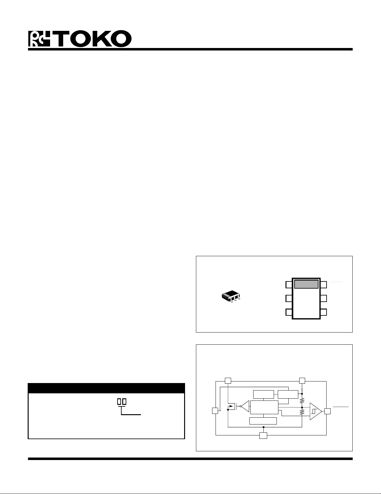
TK65025M
M25
BLOCK DIAGRAM
1
V
IN
2 5
GND
3
IND
6
4
RESET
GND
V
OUT
2
ORDERING INFORMATION
TK65025M
TAPE/REEL CODE
BX : Bulk/Bag
TL : Tape Left
February, 1997 Toko, Inc. Page 1
Tape/Reel Code

TK65025
ABSOLUTE MAXIMUM RATINGS
All pins except GND................................................... 6 V
Power Dissipation (Note1) ................................. 400 mW
Storage Temperature Range ................... -55 to +150 °C
ELECTRICAL CHARACTERISTICS
Over operating temperature range and supply voltage range, unless otherwise specified.
SYMBOL PARAMETER TEST CONDITION MIN TYP MAX UNIT
Operating Temp. Range............................-20 to + 80 °C
Junction Temperature ...........................................150 °C
V
IN
I
B(Q)
I (VIN) Quiescent current into VIN pin V
I (V
ƒ
∆ƒ
V
∆V
∆V
∆V
V
V
V
∆V
R
D
) Quiescent current into V
OUT
(OSC)
(OSC)/
OUT(REG)
∆T Temperature stability of V
OUT/
OUT(LOAD)
OUT(LINE)
OUT(RST)
RST(HI)
RST(LO)
OUT(RST)VOUT(RST)
SW(ON)
(OSC)
Supply Voltage Range (Note 2, 5) 0.90 1.60 V
No Load Battery Current (Note 5) VI = 1.3 V, IO = 0 mA, TA = 25 °C 80 120 µA
= 1.3 V IO = 1mA, TA = 25 °C 2035µA
IN
OUT
pin V
OUT
= V
OUT (REG)
+20 mV, TA = 25 °C22 34µA
Internal oscillator frequency TA = 25 °C 70 83 102 kHz
∆T Temperature stability of oscillator VIN = 1.3 V , IO = 1mA 800 ppm/°C
Regulation threshold of V
OUT
OUT(REG)VIN
Load regulation of V
Line regulation of V
V
during reset transition VIN = 1.3 V, TA = 25 °C 2.48 2.70 V
OUT
OUT(REG)
OUT(REG)
Logic High of RESET w/r/t V
(Note 2) VIN = 1.3 V, IO = 0→4 mA 0 mV
OUT
TA = 25 °C 2.85 3.00 3.10 V
= 1.3 V, IO = 1mA 250 ppm/°C
∆V
= 0.25 V, IO = 1mA -20 0 20 mV
IN
VO ≥ 2.6 V -100 mV
Logic Low of RESET VO ≤ 2.5 V 100 mV
threshold hysteresis TA = 25 °C45mV
On-resistance of switch, IND pin V
OUT
= V
OUT(REG), TA
= 25 °C 1 ohm
On-time duty ratio of oscillator 36 50 64 %
η Converter efficiency (Notes 4,5) VI = 1.3 V, IO = 4 mA 74 %
V
UVL
I
O(MAX)
Undervoltage lockout threshold TA = 25 °C IO = 1mA 0.74 V
Maximum IO for converter (Notes 3,5) VI ≥ 1.1 V, VO Regulated 4 mA
Note 1: Derate at 0.8 mW/oC for operation above TA = 25 oC ambient tempera-
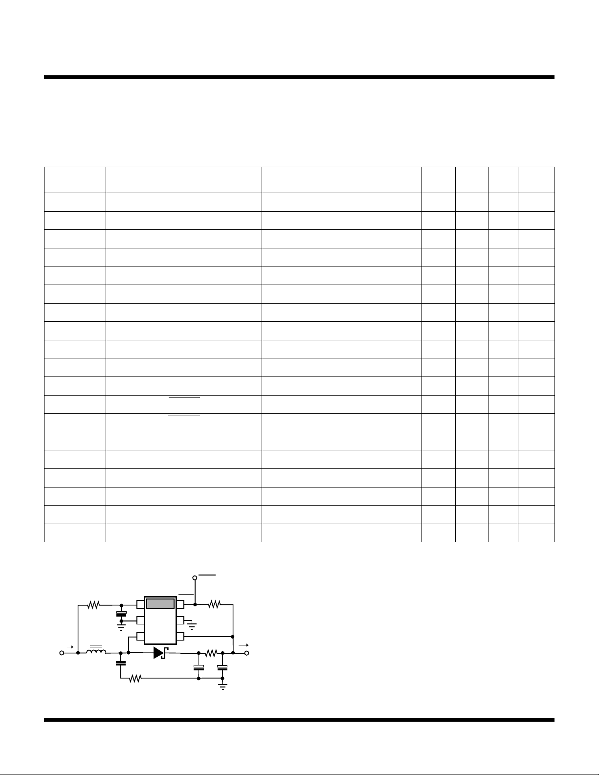
TEST CIRCUIT
R
N
C
1K
10 µF
L
I
V
I
Inductor L: Toko 682AE-014 or equivalent
Diode D: LL103A or equivalent
Capcitors CN: CU; CD: Panasonic TE series, ECS-T0JY106R
= 95 µH
B
S
C
V
IN
1
S
+
N
GND
2 5
S
IND
3
S
S
220 pF
S
D
R
S
1K
RESET
6
GND
V
OUT
4
C
10 µF
RESET
R
R
S
300 kΩ
S
S
+
C
10 µF
IO
D
R
OF
S
+
15
U
S
ture, when heat conducting copper foil path is maximized on the printed circuit
board. When this is not possible, a derating factor of 1.6 mW/ °C must be used.
Note 2: Specifications are tested to 1.6 V. Device is suitable for dual cell
operation.
Note 3: Maximum load current depends on inductor value. With a 0.9 V or 1.0
V supply voltage, 4 mA can be obtained with a smaller inductor value.
V
O
Note 4: Output ripple depends on filter capacitor values, ESRs and the
connection of (V
) sense point.
OUT
Note 5: When using specified TOKO inductor and Schottky diode with VF=0.45
V @ 100 mA. By trading component size for better specifications, using
Schottky diode with lower forward voltage, efficiency greater than 80% can be
attained.
Page 2 February, 1997 Toko, Inc.

(V)
M
A
BATTERY CURRENT
vs INPUT VOLTAGE
0 .5 1.5
VI(V)
I
B
(µA)
10
200
2 2.5 3
100
7
1
TA = 25 °C
No Load
V
TK65025
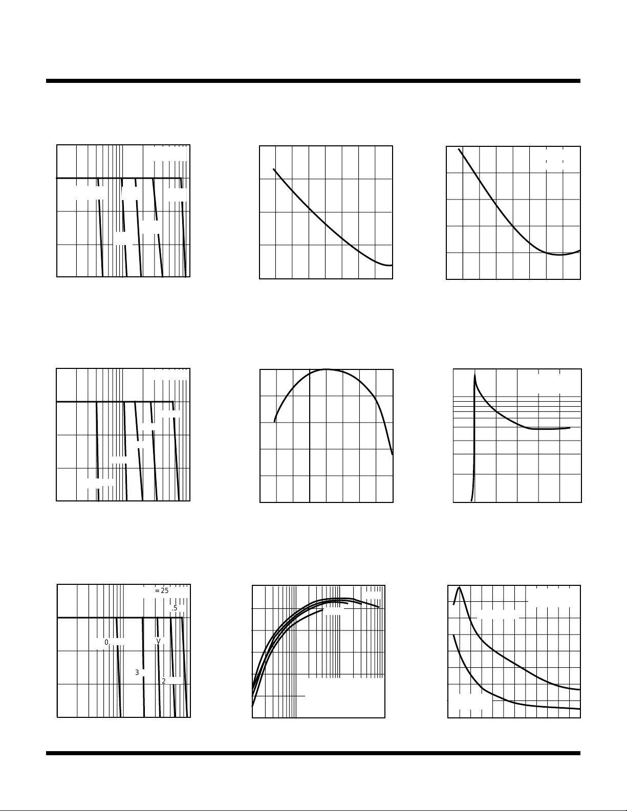
TYPICAL PERFORMANCE CHARACTERISTICS
OUTPUT VOLTAGE
vs. LOAD CURRENT
3.1
3.0
V
:
0.9 V
IN
2.9
O
2.8
1.3 V
TA = 25 °C
1.6 V
2.0 V
2.5 V
L = 100 µH
Toko P/N: 636CY101M
(D73 series)
(kHz)
ƒ
OSCILLATOR FREQUENCY vs.
95
90
85
(OSC)
90
TEMPERATURE
BATTERY CURRENT vs.
TEMPERATURE
110
100
90
(µA)
B
I
80
70
VIN = 1.3 V
No Load
2.7
110
I
(mA)
O
100
4
OUTPUT VOLTAGE
vs. LOAD CURRENT
3.1
3.0
(V)
2.9
O
V
2.8
2.7
110
1.3 V
0.9 V
V
:
in
I
O
(mA)
TA = 25 °C
2.5 V
2.0 V
1.6 V
100
5
L = 95 µH
Toko P/N:
A682AE014=P3
(3DF series)
OUTPUT VOLTAGE
vs. LOAD CURRENT
3.1
3.0
TA = 25 °C
2.5 V
L = 47 µH
Toko P/N:
636FY-470
(D73 series)
(V)
2.9
O
V
2.8
2.7
110
VIN :
0.9 V
I
O
1.3 V
(mA)
1.6 V
2.0 V
100
6
75
-75 -25 25 75
OUTPUT REGULATION VOLTAGE
vs. TEMPERATURE
3.000
2.995
(V)
2.990
2.985
OUT(REG)
V
2.980
2.975
-75 -25 25 75
TA(°C)
EFFICIENCY vs. LOAD CURRENT
90
85
80
75
η(%)
70
65
60
0.1 1
ROF = 0
L = 100 µH
Toko P/N 636CY-101M
D73 Series
TA = 25 °C
IO(mA)
TA(°C)
0.9 V
10
2.5 V
100
125
2
125
1
8
60
-75 -25
MAXIMUM OUTPUT CURRENT vs.
16
14
12
10
OUTPUT CURRENT (mA)
INDUCTOR VALUE (µH)
VIN = 1.3 V
8
6
4
2
VIN = 0.9 V
0
0 80 240 400
INDUCTOR VALUE (µH)
25 75
TA(°C)
160 320 440
V
= 2.5 V
OUT
TA = 25 °C
125
3
2
9
February, 1997 Toko, Inc. Page 3

TK65025
SINGLE-CELL APPLICATION
The TK65025 is a boost converter control IC with the
power MOSFET switch built into the device. It operates
from one or two battery cells and steps up the output
voltage to a regulated 3.0 Volts. The device operates at a
fixed nominal clock frequency of 83 kHz. The analysis is
easier to follow when referencing the test circuit below.
RESET
R
N
C
1K
10 µF
L
I
V
I
= 95 µH
B
S
C
V
IN
1
S
+
N
GND
2 5
S
IND
3
S
S
220 pF
S
R
S
1K
RESET
6
GND
V
OUT
4
D
10 µF
R
R
S
300 kΩ
S
S
+
C
10 µF
IO
V
O
D
R
OF
S
+
15
C
U
S
The Test Circuit shown here is identical with the one
shown on page 2 of the TK65025 data sheet.
RIPPLE AND NOISE CONSIDERATIONS
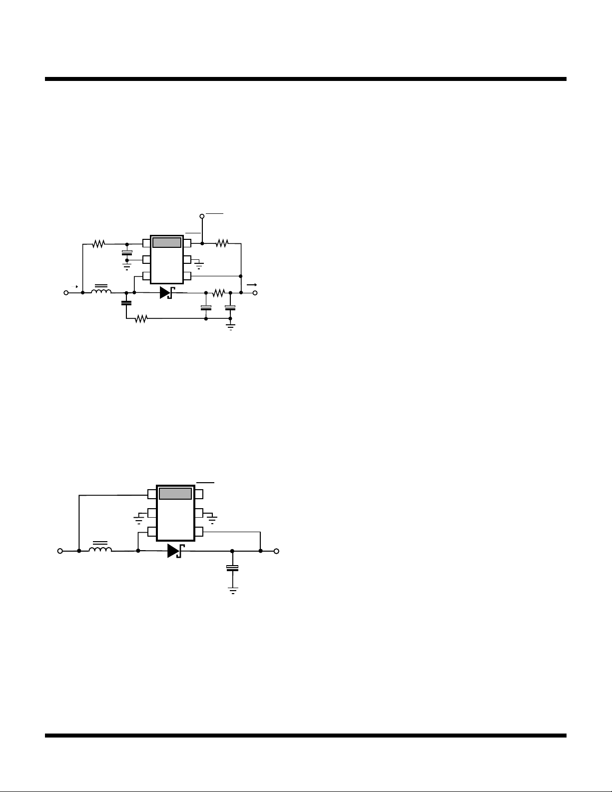
In its simplest form, a power converter using the TK65025
requires only three external components: an inductor, a
diode, and a capacitor (see figure below).
V
IN
1
GND
2 5
IND
3
V
S
I
S
Compared to the test circuit, this means eliminating the
following circuitry: the RC filter into the Vin pin, the RC
snubber, the RC filter at the converter output, and the
pullup resistor to the reset pin. The RC filter at the Vin pin
is used only to prevent the ripple voltage at the battery
terminals from prematurely causing under-voltage lockout
of the IC. This is only needed when the inductor value is
relatively small and the battery resistance is relatively high
and the Vin range must extend as low as possible. The RC
RESET
6
GND
V
OUT
4
V
O
S
S
+
snubber dampens the ringing which occurs during the
deadtime, but this provides only a limited noise reduction,
so it isn’t required. The RC filter at the converter output
attenuates the conducted noise - the converter doesn’t
require this either. Finally, the pullup resistor at the reset
pin is needed only if the reset output signal is used. Most
of this circuitry which appears in the test circuit has been
added to minimize ripple and noise effects. But when this
is not critical, the circuit can be minimized.
When any DC-DC converter is used to convert power
in RF circuits (e.g., pagers) the spectral noise generated
by the converter, whether conducted or radiated, is of
concern. The oscillator of the TK65025 has been trimmed
and stabilized to 83 +/– 4 kHz with the intention of greatly
minimizing interference at the common IF frequency of
455 kHz. In comparison with conventional IC solutions,
where the oscillator frequency is not controlled tightly, the
TK65025 can achieve as much as 20-30 dB improvements in RF interference reduction by means of its accurately controlled oscillator frequency. This IF frequency is
halfway between the fifth and sixth harmonics of the
oscillator. The fifth harmonic of the maximum oscillator
frequency and the sixth harmonic of the minimum oscillator frequency still leave a 39 kHz band centered around
455 kHz within which a fundamental harmonic of the
oscillator will not fall. Since the TK65025 operates by
pulse burst modulation (PBM), the switching pattern can
be a subharmonic of the oscillator frequency. The simplest example and the one most to be avoided is that of the
converter causing every other oscillator pulse to be skipped.
That means that the switching pattern would have a
fundamental frequency of one-half the oscillator frequency,
or 41.5 kHz - the eleventh harmonic of which lands at
456.5 kHz, right in the IF band. Fortunately, the energy is
rather weak at the eleventh harmonic - and even more
fortunate is the ease with which that regulation mode is
avoided. Due to a finite hysteresis in the regulator comparator, when an additional output filter is used (e.g., the
RC filter of the test circuit, or an LC filter) this minimizes the
ripple at the regulation node which limits the rate at which
the oscillator can be gated. In practice, this means that
rather than exhibiting a switching pattern of skipping every
other oscillator pulse, it would be more likely to exhibit a
switching pattern of three or four pulses followed by that
many pulses skipped. Although this also tends to increase
the output ripple, it is low frequency and has low magnitude (e.g., 10 kHz and 10 mV) which tends to be of little
consequence.
Page 4 February, 1997 Toko, Inc.
 Loading...