TOKO TK65020MTL Datasheet
ADVANCED INFORMATION
V
IN
GND
SW
NC
V
OUT
CONTROL
CIRCUIT
OSCILLATOR
Vref UVLO
20P
TK65020
ADVANCED
INFORMATION
FEATURES
■ Guaranteed 0.9 V Operation
■ Very Low Quiescent Current
■ Internal Bandgap Reference
■ High Efficiency MOS Switching
■ Low Output Ripple
■ Laser-Trimmed Output Voltage
■ Laser-Trimmed Oscillator
■ Undervoltage Lockout
■ Regulation by Pulse Burst Modulation (PBM)
DESCRIPTION
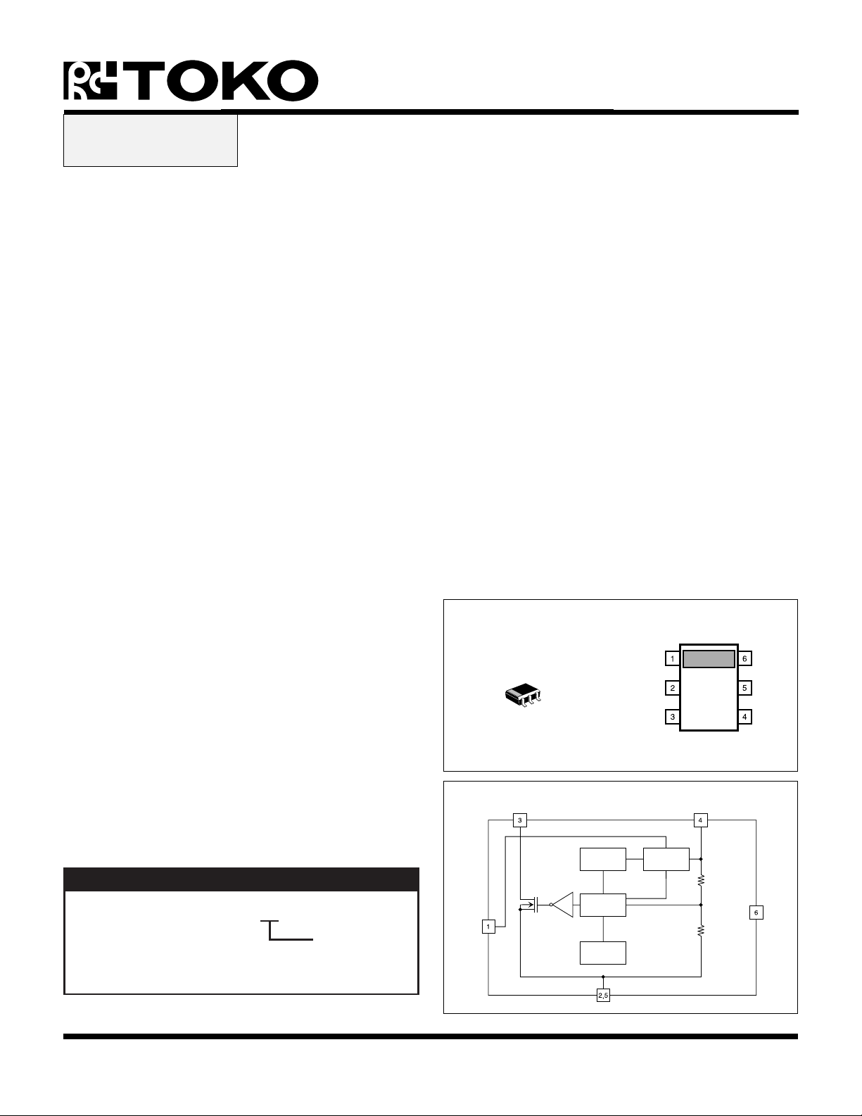
The TK65020 low power step-up DC-DC converter is
designed for portable battery-powered systems, capable
of operating from a single battery cell down to 0.9 V. The
TK65020 provides the power switch and the control circuit
for a boost converter. The converter takes a DC input and
boosts it up to a regulated 2.5 V output .
STEP-UP VOLTAGE CONVERTER
APPLICATIONS
■ Battery Powered Systems
■ Cellular Telephones
■ Pagers
■ Personal Communications Equipment
■ Portable Instrumentation
■ Portable Consumer Equipment
■ Radio Control Systems
taken to achieve reliability through the use of Oxide,
double Nitride passivation. The TK65020 is available in a
miniature 6-pin SOT-23L-6 surface mount package.
For other output levels, please refer to the TK651xx and
TK652xx Toko series of step-up converters.
The output voltage is laser-trimmed. An internal
Undervoltage Lockout (UVLO) circuit is utilized to prevent
TK65020
the inductor switch from remaining in the “on” mode when
the battery voltage is too low to permit normal operation.
V
IN
NC
Pulse Burst Modulation (PBM) is used to regulate the
voltage at the V
pin of the IC. PBM is the process in
OUT
which an oscillator signal is gated or not gated to the switch
drive each period. The decision is made just before the
GND
SW
GND
V
OUT
start of each cycle and is based on comparing the output
voltage to an internally-generated bandgap reference.
The decision is latched, so the duty ratio is not modulated
within a cycle. The average duty ratio is effectively
modulated by the “bursting” and skipping of pulses which
BLOCK DIAGRAM
can be seen at the SW pin of the IC. Special care has been
ORDERING INFORMATION
TK65020MTL
Tape/Reel Code
TAPE/REEL CODE
TL: Tape Left
January 1999 TOKO, Inc. Page 1
TK65020
ADVANCED INFORMATION
ABSOLUTE MAXIMUM RATINGS
All Pins Except SW and GND .................................... 6 V
SW Pin ....................................................................... 9 V
Power Dissipation (Note 1) ................................. 400 mA
Storage Temperature Range ................... -55 to +150 °C
Operating Temperature Range ...................-20 to +80 °C
Junction Temperature ...........................................150 °C
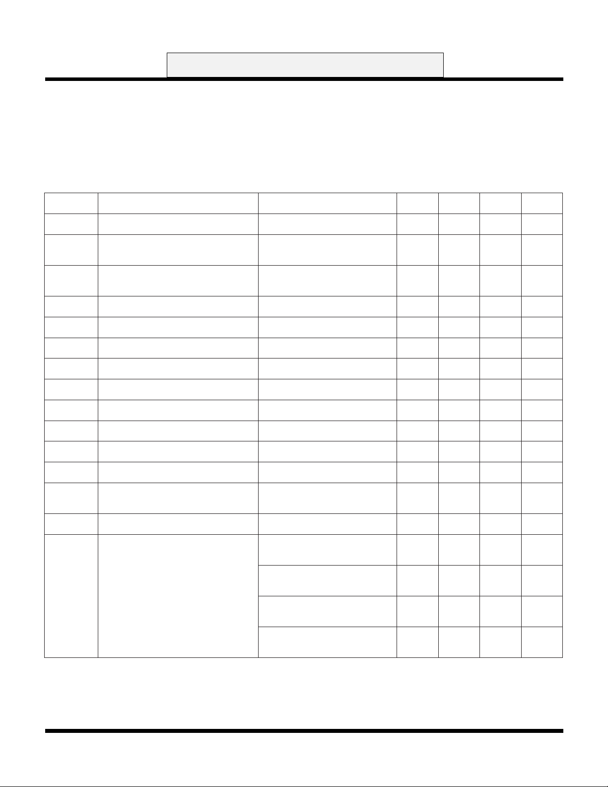
TK65020 ELECTRICAL CHARACTERISTICS
Over operating temperature range and supply voltage range, unless otherwise specified.
LOBMYSRETEMARAPSNOITIDNOCTSETNIMPYTXAMSTINU
V
NI
I
)Q(B
V(I
)VotnitnerruCtnecseiuQ
NI
)VotnitnerruCtnecseiuQ
V(I
TUO
f
CSO
∆f
/∆T
CSO
D
CSO
V
∆V
/∆T
TUO
∆V
∆V
R
)NO(WS
FFE)4,3setoN(ycneiciffEretrevnoC
egatloVylppuS09.006.1V
V
NI
)3etoN(tnerruCyrettaBdaoLoN
T
A
V
niP
NI
niPVNI,V3.1=I
TUO
ycneuqerFrotallicsOlanretnIV
rotallicsOfooitaRytuDemit-nOT
)GER(TUO
VfodlohserhTnoitalugeR
TUO
VfoytilibatSerutarepmeT
)DAOL(TUO
)ENIL(TUO
VfonoitalugeRdaoL
VfonoitalugeReniL
)GER(TUO
)GER(TUO
niPWSfoecnatsiser-nOT
NI
T
A
NI
rotallicsOfoytilibatSerutarepmeTV
NI
A
T
A
V
)GER(TUO
NI
V
NI
∆V
NI
≥ 4.20.1V
A
V
NI
,V3.1=I
TUO
C°52=
,V3.1=I
TUO
C°52=
TUO
,V3.1=I
TUO
,V3.1=
C°52=540555%
C°52=83.205.285.2V
,V3.1=I
TUO
,V3.1=I
TUO
V52.0=
,V3.1=I
TUO
,Am0=
,Am0=
1426Aµ
1102Aµ
Am0=2102Aµ
Am0=0738201zHk
gnippikSesluPoN
1.0C°/%
Am0=001Vm
Am4ot0=005Vm
02-03Vm
,Am6=
lioCFD3,Hµ59=L
67%
V
VLU
ImumixaM
I
)XAM(TUO
Note 1: Derate at 0.8 mW/oC for operation above TA = 25 oC ambient temperature, when heat conducting copper foil path is maximized on the printed
circuit board. When this is not possible, a derating factor of 1.6 mW/ °C must be used.
TUO
)4,2setoN(
egatloVtuokcoLegatlovrednUT
A
V
NI
T,V1.1=
)5etoN(,C°52=54.097.0V
A
,C°52=
lioCFD3,Hµ59=L
V
NI
retrevnoCrof
V
NI
T,V3.1=
A
,C°52=
lioCFD3,Hµ59=L
T,V1.1=
A
,C°52=
lioC37D,Hµ93=L
V
NI
T,V3.1=
A
,C°52=
lioC37D,Hµ93=L
50.8Am
90.51Am
8.91Am
0.83Am
Page 2 January 1999 TOKO, Inc.
ADVANCED INFORMATION
TK65020
Inductor L: Toko A682AE-014 or equivalent
Diode D: LL103A or equivalent
Capacitors CN:CO:CB: Panasonic TE series,
ECS-TOJY106R
I
B
V
IN
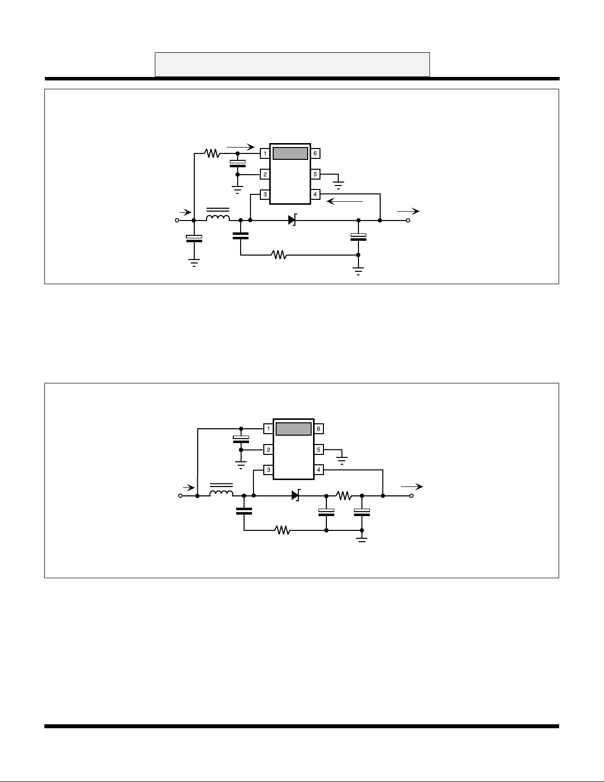
BENCH TEST CIRCUIT
I(VIN)
V
R
N
1 K
C
10 µF
L = 95 µH
C
B
10 µF
IN
GND GND
N
C
S
220 pF
1 K
R
S
NC
V
OUTIND
D
I(V
)
OUT
Note 2: Maximum load current depends on
inductor value and input voltages.
Note 3: Output ripple depends on filter
capacitor values, ESRs and the
inductor value.
Note 4: When using specified Toko inductor
and Schottky diode with VF = 0.45 V
@ 100 mA.
Note 5: Regulation not guaranteed
I
OUT
V
OUT
C
O
10 µF
The Bench Test Circuit is used most of the time to measure the typical (typ.) values in the Electrical Characteristics
section, and make the Typical Performance graphs.
Note: In measuring the oscillator frequency and the Max I
on the bench, the converter was loaded until “no pulse
OUT
skipping” mode was achieved.
FINAL TEST CIRCUIT
V
IN
GND GND
N
C
S
220 pF
R
1 K
S
I
B
V
IN
Inductor L: Toko A682AE-014 or equivalent
Diode D: LL101
Capacitors CN:CU:CD: Panasonic TE series,
C
10 µF
L = 95 µF
ECS-TOJY106R
Above is the Final Test Circuit through which each of the production parts must pass. In this test circuit, the part is tested
against the specification limits in the data sheet (the min. and max. values in the Electrical Characteristics) at room
temperature, and is rejected if the tested values are outside the minimum (min.) and maximum (max.) values.
NC
V
OUTSW
I
R
OF
15
D
++
C
U
10 µF
10 µF
OUT
V
OUT
C
D
January 1999 TOKO, Inc. Page 3
TK65020
BATTERY CURRENT
VS.
INPUT VOLTAGE
120
0 .5 1 1.5 2 2.5 3
VIN (V)
I
B
(µA)
100
60
80
40
20
0
TA = 25 °C
NO LOAD
TK65020
ADVANCED INFORMATION
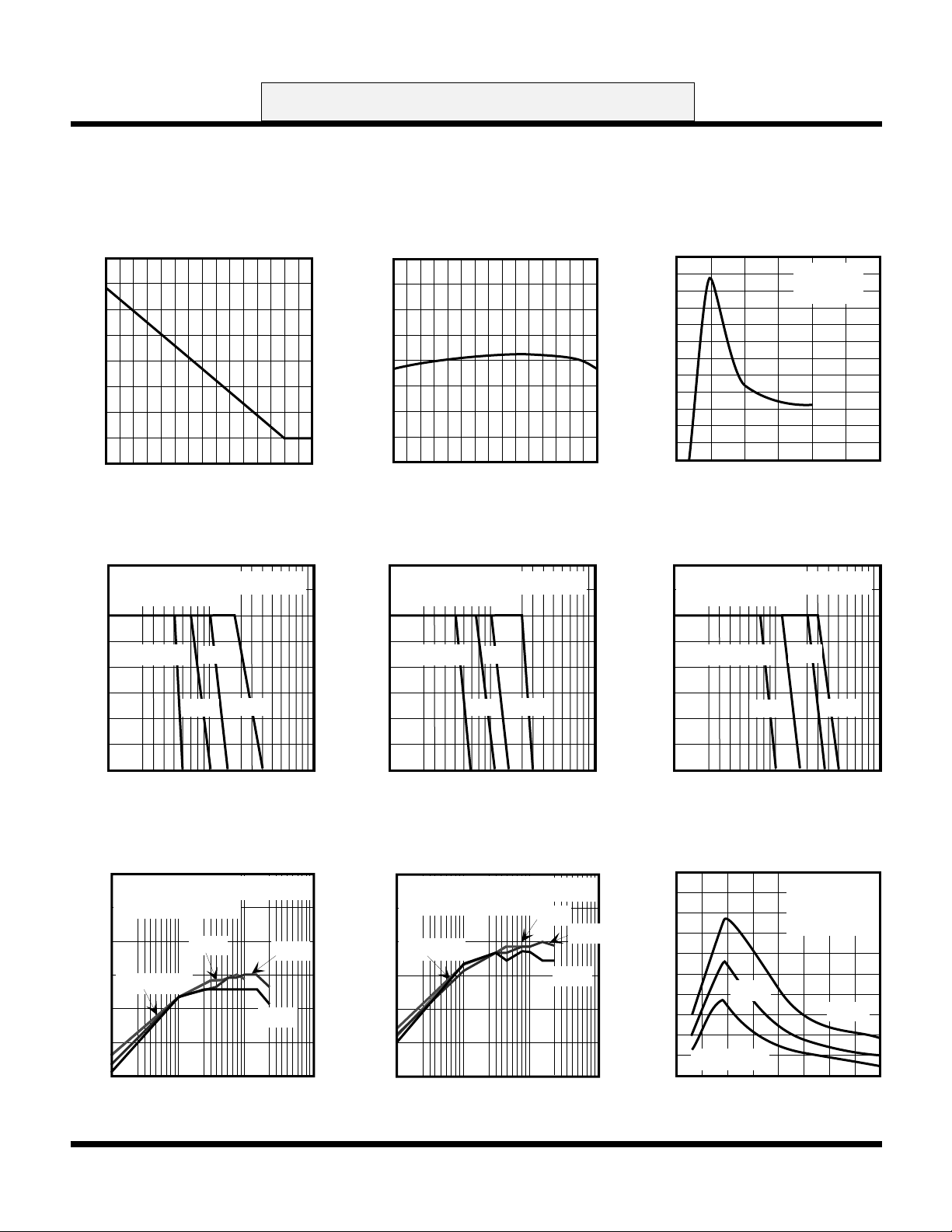
TYPICAL PERFORMANCE CHARACTERISTICS
OSCILLATOR FREQUENCY VS.
TEMPERATURE
95
90
(kHz)
85
OSC
f
80
75
-50 0 50 100
TEMPERATURE (°C)
OUTPUT VOLTAGE
2.6
L = 95 µH
TOKO P/N: A682AE-014
(3DF SERIES)
LOAD CURRENT
TA = 25 °C
2.5
(V)
OUT
V
2.4
2.3
V
IN
= 0.9 V
1.3 V
1.1 V
1.6 V
VS.
OUTPUT REGULATION VOLTAGE
TEMPERATURE
2.60
2.55
(V)
2.50
OUT(REG)
V
2.45
2.40
-50 0 50 100
TEMPERATURE (°C)
OUTPUT VOLTAGE
2.6
L = 100 µH
TOKO P/N: A636CY-101M
(D73 SERIES)
LOAD CURRENT
TA = 25 °C
2.5
(V)
OUT
V
2.4
2.3
V
IN
= 0.9 V
1.3 V
1.1 V 1.6 V
VS.
VS.
2.6
L = 39 µH
TOKO P/N: A636CY-390M
(D73 SERIES)
2.5
(V)
2.4
OUT
V
2.3
OUTPUT VOLTAGE
LOAD CURRENT
TA = 25 °C
V
IN
= 0.9 V
1.3 V
1.1 V 1.6 V
VS.
2.2
1 10 100
EFFICIENCY
90
L = 95 µF
Toko P/N: A682AE-014
(3DF SERIES) SMALL COIL
85
80
75
VIN = 0.9 V
EFF (%)
70
65
60
0.1 1 10 100
Page 4 January 1999 TOKO, Inc.
I
(mA)
OUT
VS.
LOAD CURRENT
TA = 25 °C
1.1 V
I
(mA)
OUT
1.3 V
1.6 V
2.2
1 10 100
I
(mA)
OUT
EFFICIENCY
90
L = 100 µF
Toko P/N: 636CY-101M
(D73 SERIES) LARGER COIL
85
80
V
= 0.9 V
IN
VS.
LOAD CURRENT
TA = 25 °C
1.1 V
75
EFF (%)
70
65
60
0.1 1 10 100
I
(mA)
OUT
1.3 V
1.6 V
2.2
1 10 100
I
(mA)
OUT
MAXIMUM OUTPUT CURRENT
INDUCTOR VALUE (µH)
50
NO PULSE
SKIPPING
40
(mA)
30
20
OUT(MAX)
I
1.1 V
MODE
TA = 25 °C
10
VIN = 0.9 V
0
0 40 80 120 160
INDUCTOR VALUE (µH)
VS.
1.3 V
ADVANCED INFORMATION
SINGLE-CELL APPLICATION
TK65020
The TK65020 is a boost converter control IC with the
power MOSFET switch built into the device. It operates
from a single battery cell and steps up the output voltage
to a regulated 2.5 V. The device operates at a fixed
nominal clock frequency of 83 kHz.
In its simplest form, a boost power converter using the
TK65020 requires only three external components: an
inductor, a diode, and a capacitor.
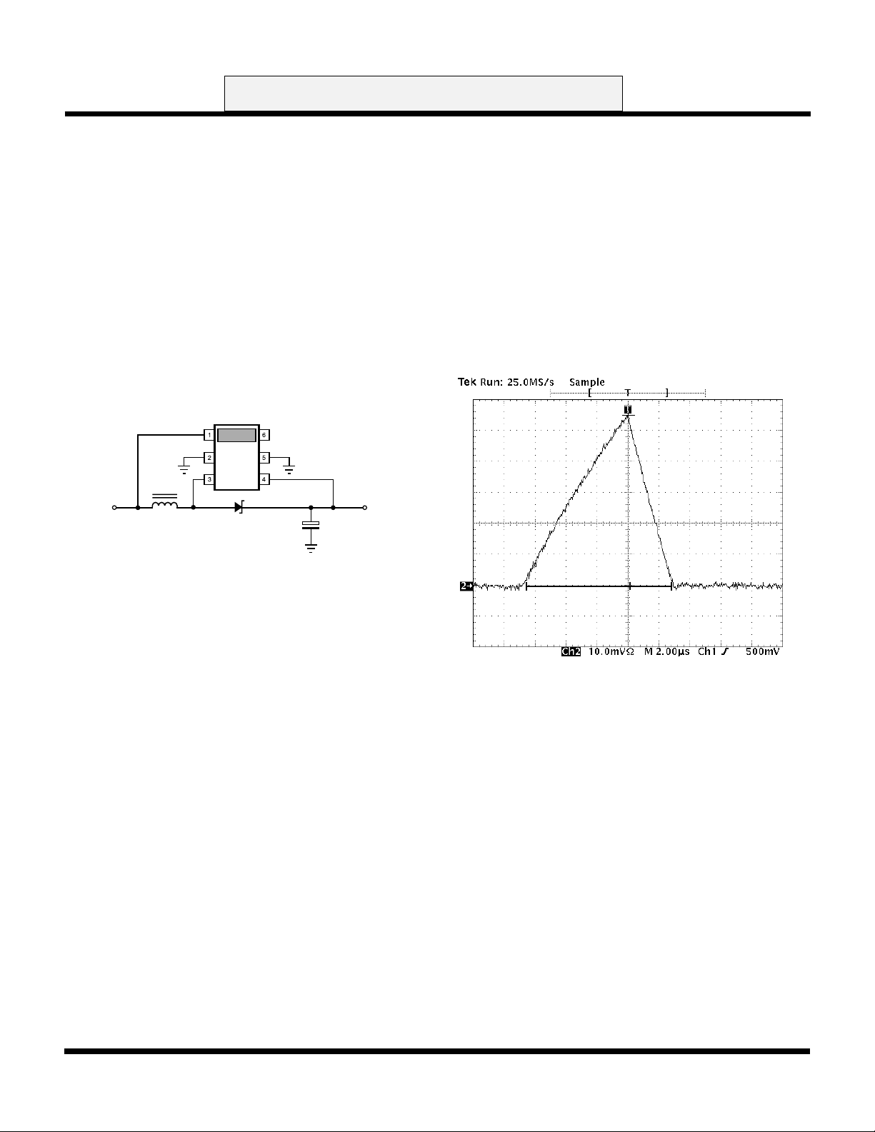
The analysis is easier to follow when referencing the
simple boost circuit below.
V
IN
GND GND
NC
V
OUTSW
V
+
OUT
FIGURE 1: SIMPLE BOOST CONVERTER
and Noise Considerations” section) can be determined if
needed or desired.
The TK65020 runs with a fixed oscillator frequency and it
regulates by applying or skipping pulses to the internal
power switch. This regulation method is called Pulse Burst
Modulation (PBM).
ANALYSIS OF SWITCHING CYCLE
I
PEAK
di/dt = VIN/ L
t (on)
di/dt = - (V
t (off)
+ Vf - VIN)/ L
OUT
t (deadtime)
THEORY OF OPERATION
The converter operates with one terminal of an inductor
connected to the DC input and the other terminal connected
to the switch pin of the IC. When the switch is turned on, the
inductor current ramps up. When the switch is turned off (or
“lets go” of the inductor), the voltage flies up as the inductor
seeks out a path for its current. A diode, also connected to
the switching node, provides a path of conduction for the
inductor current to the boost converter’s output capacitor.
The TK65020 monitors the voltage of the output capacitor
and has a 2.5 V threshold at which the converter switching
becomes deactivated. So the output capacitor charges up
to 2.5 V and regulates there, provided that no more current
is drawn from the output than the inductor can provide. The
primary task, then, in designing a boost converter with
the TK65020 is to determine the inductor value (and its
peak current rating to prevent inductor core saturation
problems) which will provide the amount of current
needed to guarantee that the output voltage will be
able to maintain regulation up to a specified maximum
load current. Secondary necessary tasks also include
choosing the diode and the output capacitor. Then the
snubber and filtering component values (consult the “Ripple
Above is the input or inductor current waveform over a
switching cycle.
From an oscillator standpoint, the switching cycle consists
of only an on-time and an off-time. But from an inductor
current standpoint, the switching cycle breaks down into
three important sections: on-time, off-time, and deadtime.
The on-time of the switch and the inductor current are
synonymous. During the on-time, the inductor current
increases. During the off-time, the inductor current
decreases as it flows into the output. When the inductor
current reaches zero, that marks the end of the inductor
current off-time. For the rest of the cycle, the inductor
current remains at zero. Since no energy is being either
stored or delivered, that remaining time is called “deadtime.”
This mode of the inductor current decaying to zero every
cycle is called “discontinuous mode.” In summary, energy
is stored in the inductor during on-time, delivered to the
output during off-time, and remains at zero during deadtime.
January 1999 TOKO, Inc. Page 5
 Loading...