TOKO TK65015MTL, TK65015MBX Datasheet

V
V
V
G
T
FEATURES
■ 0.9 V Operation
■ Very Low Quiescent Current
■ Internal Bandgap Reference
■ High Efficiency
■ Low Output Ripple
■ Microprocessor Reset Output
■ Laser-Trimmed Output Voltage
■ Undervoltage Lockout
■ Regulation by Pulse Burst Modulation (PBM)
TK65015
STEP-UP VOLTAGE CONVERTER
WITH VOLTAGE MONITOR
APPLICATIONS
■ Battery Powered Systems
■ Cellular Telephones
■ Pagers
■ Personal Communications Equipment
■ Portable Instrumentation
■ Portable Consumer Equipment
■ Radio Control Systems
DESCRIPTION
The TK65015 Low Power Step-Up DC-DC converter is
designed for portable battery powered systems, capable of
operating from a single battery cell down to 0.9 V.
The output voltage is laser-trimmed to 3.0 V. An internal
detector monitors the output voltage and provides an
active-low microprocessor reset signal whenever the output voltage falls below an internally preset limit. An internal
undervoltage lockout circuit is utilized to prevent the inductor switch from remaining in the "ON" mode when the
battery voltage is too low to permit normal operation.
Special care has been taken to achieve high reliability
through the use of Oxide, Nitride passivation and an
additional polyimide coating. The TK65015 is available in a
very small plastic surface mount package. (SOT-23L)
Pulse burst modulation (PBM) is used to regulate the
voltage at the V
which an oscillator signal is gated or not gated to the switch
drive each period. The decision is made just before the start
of each cycle and is based on comparing the output voltage
to an internally-generated bandgap reference. The decision is latched, so the duty ratio is not modulated within a
cycle. The average duty ratio is effectively modulated by
pin at the IC. PBM is the process in
OUT
the "bursting" and skipping of pulses which can be seen at
the IND pin of the IC.
The TK65015 provides the power switch and the control
circuit for a boost converter. The converter takes a DC
input (typically a single battery cell) and boosts it up to 3
volts. This regulated 3 volt output is typically used to supply
power to a microprocessor-controlled system.
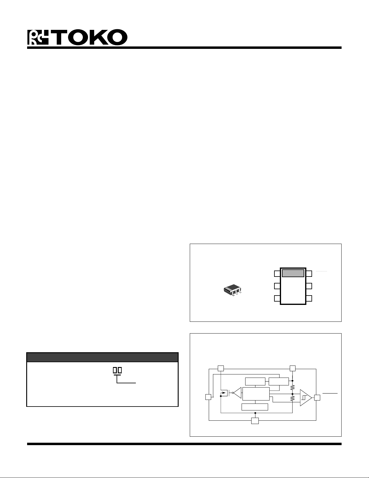
TK65015M
M15
1
IN
2 5
ND
3
IND
6
RESE
GND
V
4
O
BLOCK DIAGRAM
2
ORDERING INFORMATION
TK65015M
Tape/Reel Code
IN
TAPE/REEL CODE
BX : Bulk/Bag
TL : Tape Left
IND
3 4
V
REF
CONTROL
1
CIRCUIT
RC OSC.
2,5
GND
UVLO
O
RESET
6
February, 1996 TOKO, Inc. 2-2-96 Page 1

TK65015
V
ABSOLUTE MAXIMUM RATINGS
All pins except GND................................................... 6 V
Power Dissipation (Note1) ................................. 400 mW
Storage Temperature Range ................... -55 to +150 °C
ELECTRICAL CHARACTERISTICS
Over operating temperature range, unless otherwise specified.
VARIABLE PARAMETER TEST CONDITION MIN TYP MAX UNIT
Operating Temp. Range............................-10 to + 50 °C
Lead Soldering Temperature (10 s) ......................240 °C
Junction Temperature ...........................................150 °C
V
IN
V
UVL
I (VIN) Quiescent current into VIN pin V
I (V
ƒ
) Quiescent current into V
OUT
(OSC)
Supply Voltage range 0.90 1.60 V
Undervoltage lockout threshold TA = 25 °C .74 V
= 1.3 V 20 35 µA
IN
pin V
OUT
OUT
= V
OUT (REG)
+20 mV 22 34 µA
Internal oscillator frequency VIN = 0.9 V & VIN = 1.6 V 70 83 102 kHz
Temperature stability of oscillator VIN = 1.3 V 800 ppm/°C
D
(OSC)
V
OUT(REG)
∆V
OUT(LINE)
∆V
O (LOAD)
V
OUT(RST)
∆V
OUT(RST)VOUT(RST)
V
RST(HI)
V
RST(LO)
R
SW(ON)
I
I(Q)
I
O(MAX)
On-time duty ratio of oscillator VIN = 0.9V & V
Regulation threshold of V
Temperature stability of V
Line regulation of V
Load regulation of V
V
during reset transition 2.48 2.70 V
OUT
OUT
OUT(REG)
OUT(REG)
OUT(REG)
(Note 2) 0mA < IO < 4mA 0 mV
VIN = 0.9 V & V
VIN = 1.3 V 250 ppm/°C
V
= 0.9 V & VIN = 1.6 V -20 0 20 mV
IN
= 1.6 V 36 50 64 %
IN
= 1.6 V 2.85 3.00 3.10 V
IN
threshold hysteresis 45 mV
Logic High of RESET w/r/t V
OUT
300 kΩ Pullup -100 mV
Logic Low of RESET 300 kΩ Pullup 100 mV
On-resistance of switch, IND pin V
OUT
= V
OUT(REG)
0.5 ohms
Quiescent current of converter (Note 5) VI = 1.3 V, IO = 0mA 80 120 µA
Maximum IO for converter (Notes 3,5) VI ≥ 1.1 V, VO Regulated 4 mA
η Converter efficiency (Notes 4,5) VI = 1.3 V, IO = 4 mA 74 %
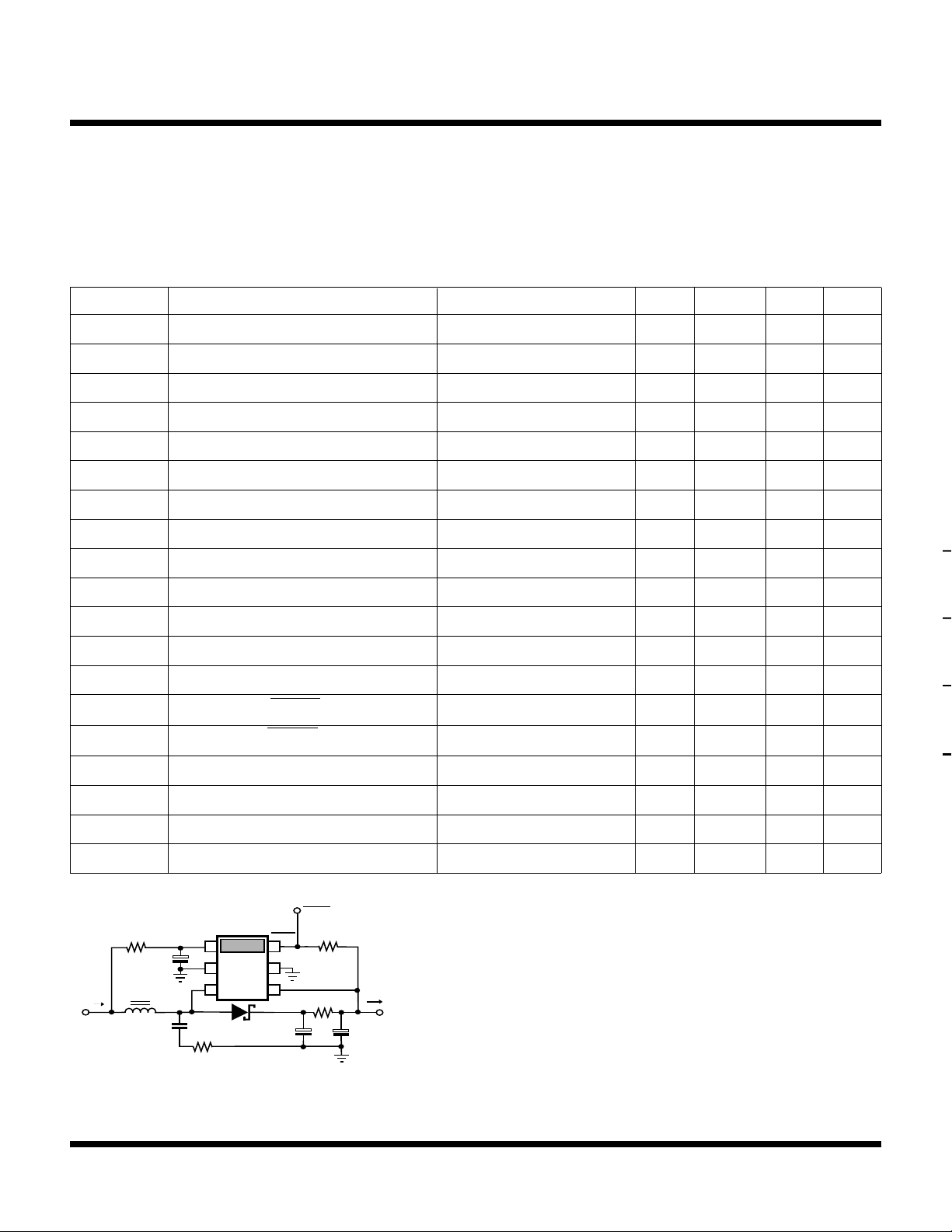
TEST CIRCUIT
1K
C
10 µF
L
= 95 µH
I
I
S
I
220 pF
V
IN
S
+
S
GND
S
IND
S
S
1K
1
2 5
3
D
RESET
6
GND
V
OUT
4
10 µF
RESET
ture, when heat conducting copper foil path is maximized on the printed circuit
board. When this is not possible, a derating factor of 1.6 mW/ °C must be used.
S
300 kΩ
15
S
+
C1
S
IO
V
+
10 µF
O
C2
S
S
Note 2: The output regulation threshold, V
be independent of the load. Regulation will occur provided that the load current is
within the capability of the converter, I
slightly with load due to the variation of the ripple voltage, whose magnitude is
OUT(REG)
O(MAX).
primarily determined by the inductor and the ESR of the output capacitors.
Note 3: Maximum load current depends on inductor value. With a 0.9 V or 1.0 V
supply voltage, 4 mA can be obtained with a smaller inductor value.
Note 4: Converter efficiency is a function of the diode forward voltage and
, is guaranteed-by-design to
The output voltage may fluctuate
inductor winding resistance. It may also depend in varying degree on the inductor
value and capacitor ESRs. By trading component size for better specifications,
Note 1: Derate at 0.8 mW/oC for operation above TA = 25 oC ambient tempera-
Inductor L: Toko A682AE-014=P3 or equivalent
Diode D: LL103A or equivalent
efficiency greater than 80% can be attained.
Note 5: Test performed using the test circuit below.
Page 2 2-2-96 February, 1996 TOKO, Inc.

OSCILLATOR FREQUENCY vs.
-20040
80
T
)
8
6
884
280
0
22060
100
I
V
V
V
0
.0
-20040
80
T
)
2060100
5
5
5
5
5
5
I
5
5
5
5
V
V
080240
400
I
)
160
320
440
)
2
4
864
0
6
V
0
6
2
8
V
080240
400
I
)
160
320
440
4
642
0121086
V
V
0
4
= 1 mA
O
9
9
8
8
FREQUENCY (kHz)
8
7
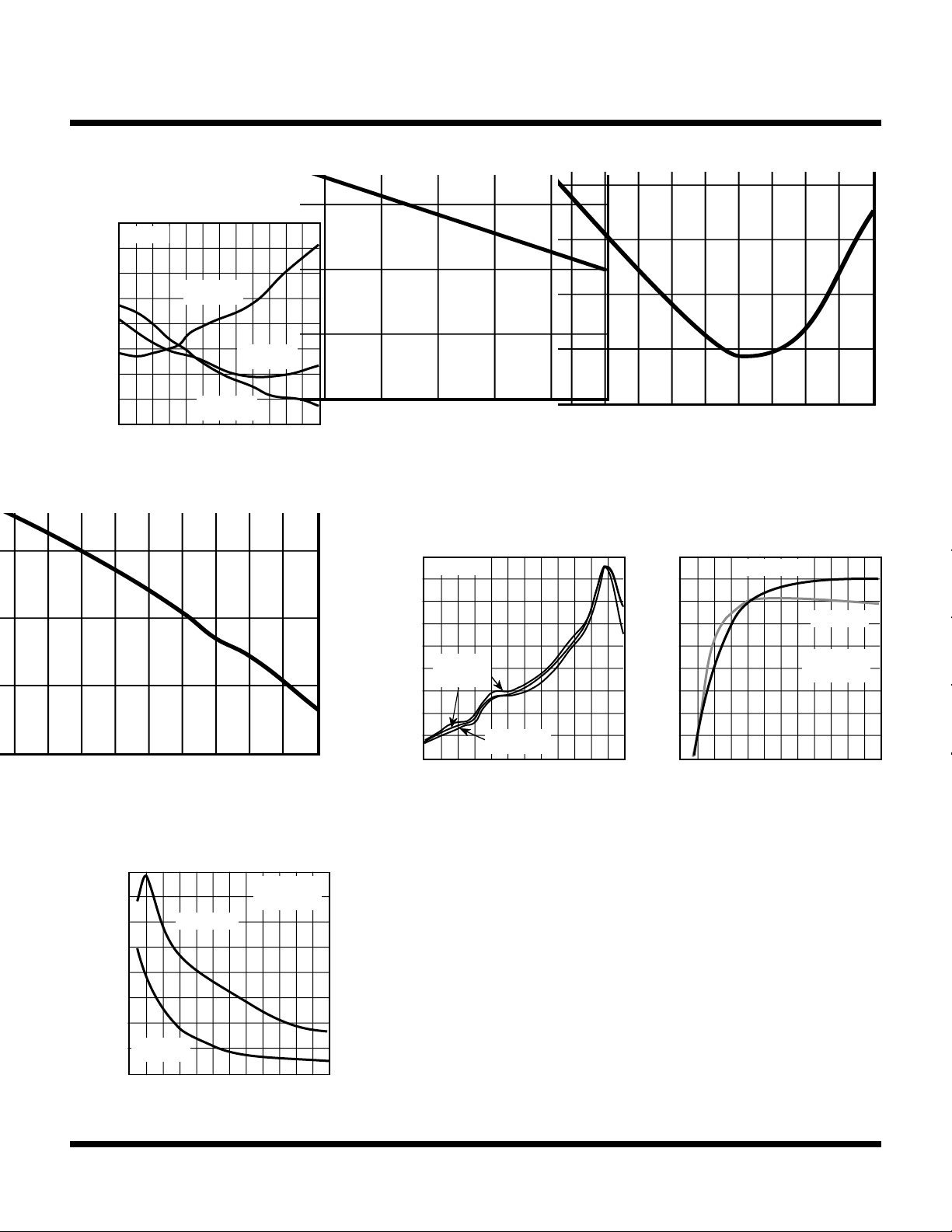
TYPICAL PERFORMANCE CHARACTERISTICS
TEMPERATURE
= 0.9 V
IN
IN
= 1.6 V
IN
EMPERATURE (°C
= 1.3 V
1.5 2.5 3.5 4
UTPUT CURRENT (mA)
1
2.0 3.0
TEMPERATURE (°C)
TK65015
20 60 10
2
40 80
2
3
20 60 10
40 80
TEMPERATURE (°C)
MAXIMUM OUTPUT CURRENT vs.
1
1
INDUCTOR VALUE (µH)
= 1.3 V
IN
V
= 2.7 V
OUT
TA = 25 °C
OUTPUT VOLTAGE vs. TEMPERATURE
3.04
= 1 mA
O
3.03
3.02
3.01
3.00
2.99
2.98
OUTPUT VOLTAGE (V)
2.97
2.96
2.95
= 1.6 V
IN
= 1.3 V
IN
VIN = 0.9 V
EMPERATURE (°C
5
EFFICIENCY vs. INDUCTOR VALUE (µH
AT MAXIMUM OUTPUT CURRENT
8
8
8
7
7
6
EFFICIENCY (%)
6
5
5
= 1.3 V
IN
NDUCTOR VALUE (µH
= 0.9 V
IN
V
= 2.7 V
OUT
TA = 25 °C
Handling Molded Resin Packages
All plastic molded packages absorb some moisture from the air. If
moisture absorption occurs prior to soldering the device into the printed
circuit board, increased separation of the lead from the plastic molding
may occur, degrading the moisture barrier characteristics of the device.
This property of plastic molding compounds should not be overlooked,
paticularly in the case of very small packages, where the plastic is very
thin.
6
OUTPUT CURRENT (mA)
= 0.9 V
IN
In order to preserve the original moisture barrier properties of the package,
devices are stored and shipped in moisture proof bags, filled with dry air.
The bags should not be opened or damaged prior to the actual use of the
NDUCTOR VALUE (µH
7
devices. Once opened the devices should be stored in a low relative
humidity environment (40 to 65%) or in an enclosed environment with
desicant.
February, 1996 TOKO, Inc. 2-2-96 Page 3
 Loading...