TK65010
01S
ADVANCED
INFORMATION
FEATURES
■ Very Low Quiescent Current ( 5 µA)
■ Dual Comparator Outputs
■ Single Monitor Input
■ Miniature Package (SOT-23-5)
DESCRIPTION
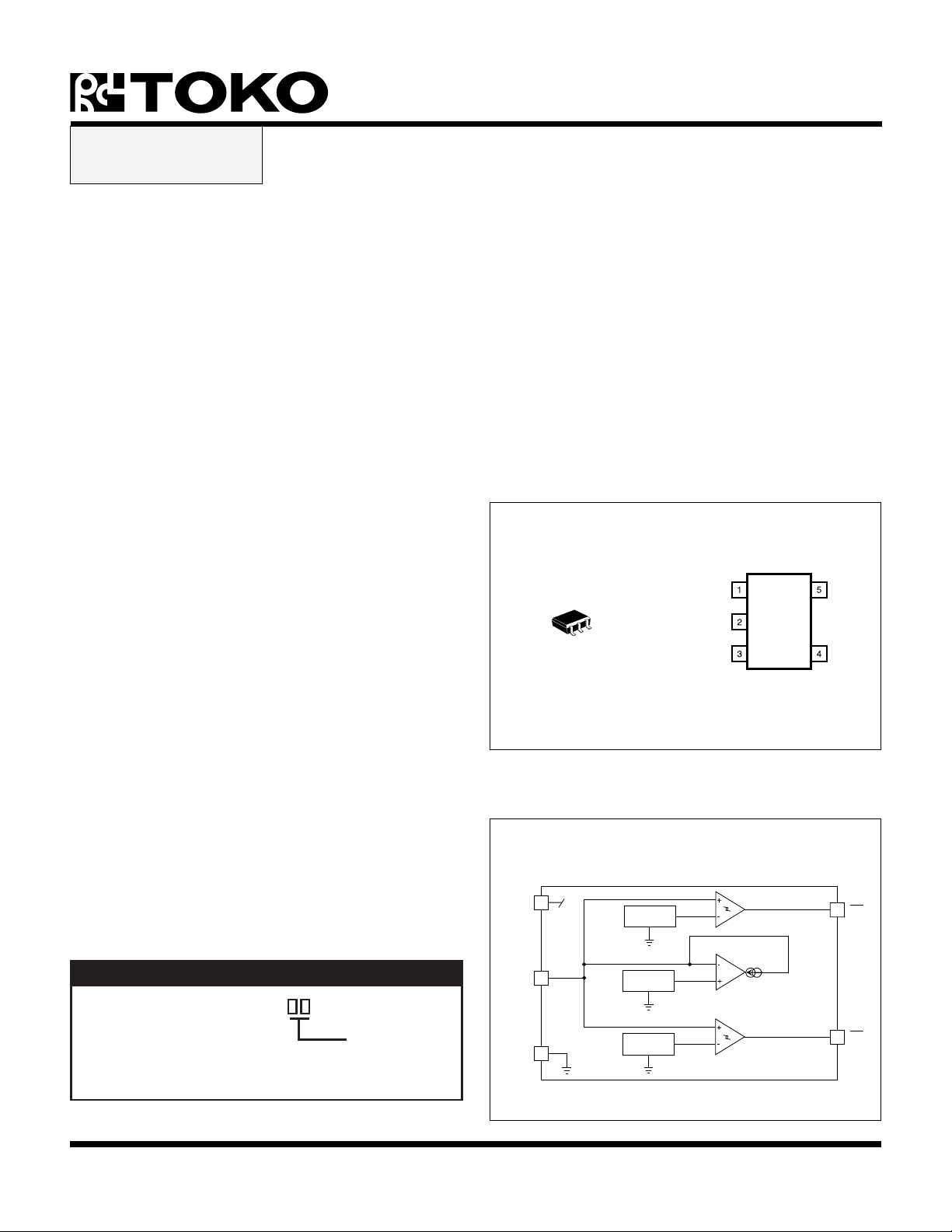
The TK65010 battery voltage monitor is designed for
portable battery powered systems where board space and
cost are important design considerations. The proprietary
monitoring architecture of the TK65010 allows two separate
warning thresholds to be set utilizing a single resistor
divider and single input pin.
The first warning indicator, a Low Battery Output (LBO), is
intended to warn the battery powered system of a low
battery condition. In such a condition, the LBO may be
used to alert the system to illuminate a low battery indicator
and to take appropriate action preparing for battery failure.
BATTERY VOLTAGE MONITOR
APPLICATIONS
■ Battery Powered Systems
■ Cellular Telephones
■ Pagers
■ Personal Communications Equipment
TK65010
V
IN
GND
V
MON
LBO
DBO
The second warning indicator, a Dead Battery Output
(DBO), is intended to be used by the system for shutdown
purposes. The availability of the DBO allows the system to
shut down in order to minimize deep discharge of the
battery.
BLOCK DIAGRAM
The two warning indicators can be implemented utilizing
the TK65010 and only two external components.
V
The TK65010 is available in a miniature 5-pin SOT-23-5
CC
710 mV
LBO
surface mount package.
ORDERING INFORMATION
V
MON
700 mV
TK65010
Tape/Reel Code
TAPE/REEL CODE
TL: Tape Left
GND
690 mV
January 1999 TOKO, Inc. Page 1
DBO

TK65010
ABSOLUTE MAXIMUM RATINGS
All Pins Except GND .................................................. 6 V
Power Dissipation (Note 1) .......................................TBD
Storage Temperature Range ................... -55 to +150 °C
TK65010 ELECTRICAL CHARACTERISTICS
VIN = 5 V, TA = Tj = Full Operating Temperature Range, unless otherwise specified.
LOBMYSRETEMARAPSNOITIDNOCTSETNIMPYTXAMSTINU
Operating Temperature Range ...................-20 to +80 °C
Junction Temperature ...........................................150 °C
V
NI
V
OBL,HT
V
AO,fer
V
OBD,HT
V
V
I
BF
I
Q
V
OBL
V
OBD
Note 1: Power dissipation is 400 mW when mounted as recommended (200 mW In Free Air). Derate at 1.6 mW/°C for operation above 25 °C.
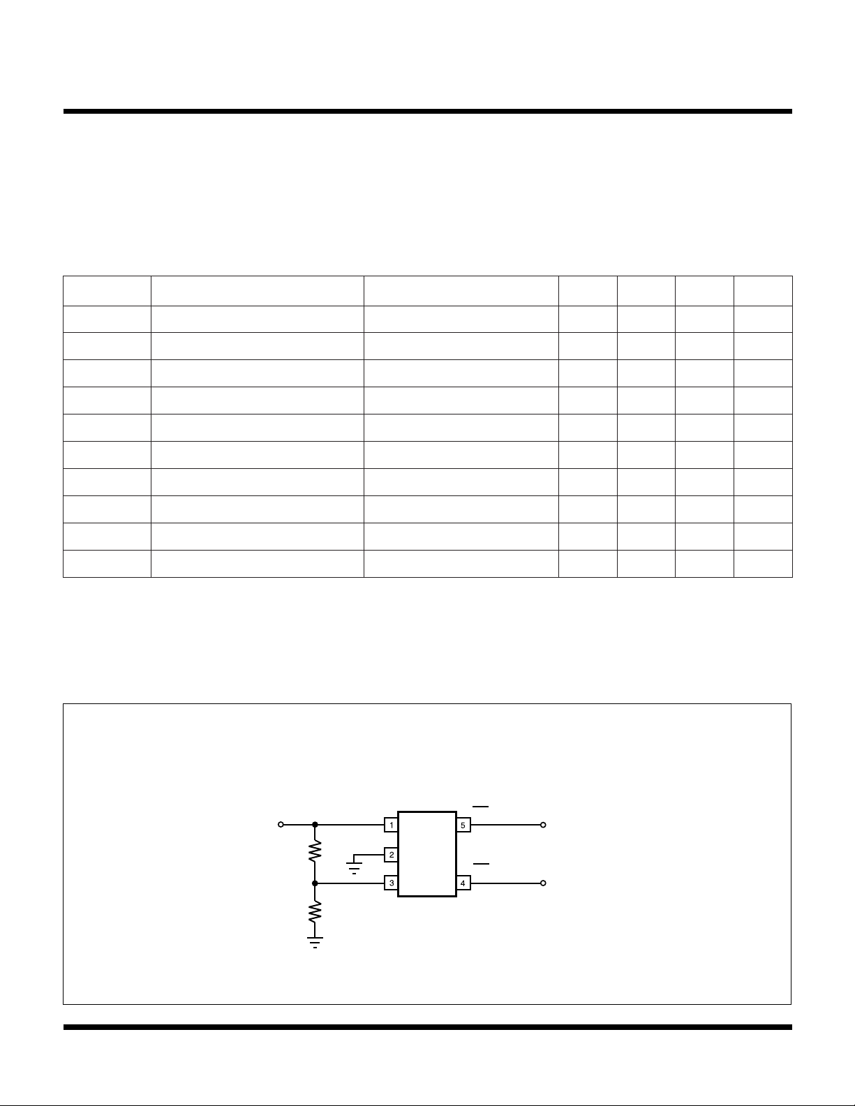
Note 2: When using test circuit below.
TSYH,OBL,HT
TSYH,OBD,HT
egnaRylppuStupnI9.06V
dlohserhTrotarapmoCOBL 017Vm
ecnerefeRpmA-PO 007Vm
dlohserhTrotarapmoCOBD 096Vm
siseretsyHrotarapmoCOBL DBTVm
siseretsyHrotarapmoCOBD DBTVm
tnerruCkcabdeeFkaePV
V=
NOM
OBL,HT
085-An
tnerruCtnecseiuQ 5Aµ
dlohserhTyrettaBwoL)2etoN(1.1V
dlohserhTyrettaBdaeD)2etoN(9.0V
TEST CIRCUIT
V
GND
V
IN
MON
BATTERY IN
R
301 K
R
1 M
1
2
Page 2 January 1999 TOKO, Inc.
LBO
LOW BATTERY
DBO
DEAD BATTERY

THEORY OF OPERATION
TK65010
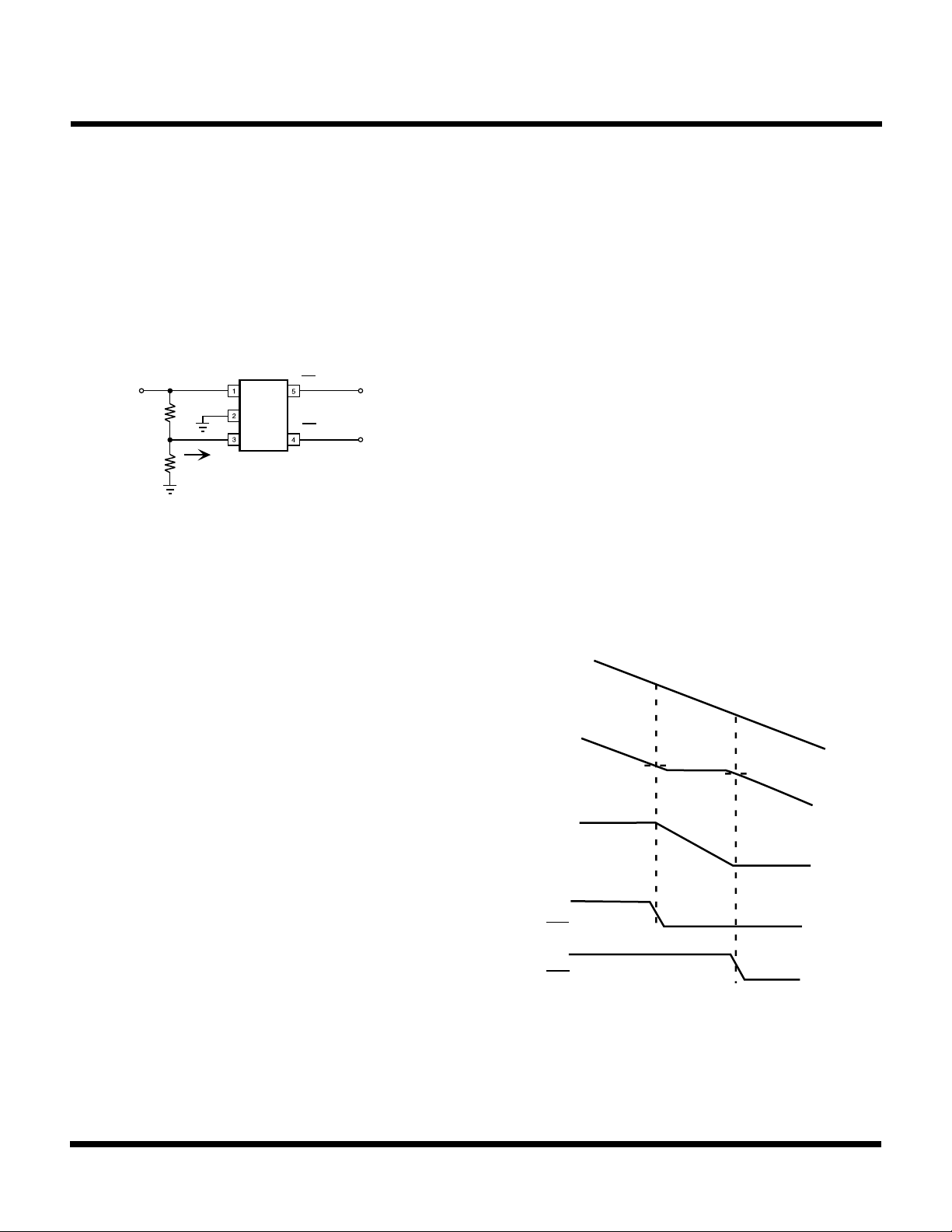
The circuit in Figure 1 illustrates a typical application
utilizing the TK65010. The TK65010 differs from most
voltage monitors due to the fact that two separate
comparator thresholds can be set utilizing a single resistive
divider and a single input pin. One comparator output is
used as an early “low battery” warning. The second
comparator can be used as a later “dead battery” warning.
BATTERY IN
R
301 K
R
1 M
IN
1
2
GND
V
MON
I
FB
LBO
DBO
LOW BATTERY
DEAD BATTERY
V
FIGURE 1
In a typical voltage monitor, which uses an external resistive
divider for setting the voltage monitor threshold, the input
bias current to the monitor pin is essentially zero. In this
type of scenario, the voltage on the monitor input would be
a resistively divided version of the battery voltage. The
TK65010 introduces a small feedback current (IFB) which
introduces a “plateau” into the transfer characteristics
between the battery voltage and the voltage monitoring
pin. The width of this plateau is dependent upon the current
range of the feedback current (IFB) and the values of the
external resistor network. Figure 2 illustrates the typical
relationship between the battery voltage (VIN), the feedback
current (IFB) and the voltage on the monitoring pin (V
MON
Under these conditions, current will be flowing into the
V
pin and will be limited to approximately 580 nA. As
MON
the battery voltage drops, the voltage on the V
drop proportionately. When the voltage on the V
passes through approximately 710 mV, the output of the
first comparator (LBO) will transition from a high to a low
state. Shortly after the LBO output has been asserted, as
the input voltage continues to drop, the magnitude of the
current into the V
pin will begin to proportionately
MON
decrease as the input voltage decreases. An op-amp
feedback loop internal to the TK65010 will attempt to
maintain the voltage on the V
pin at a constant value of
MON
approximately 700 mV (thus, the plateau). As the battery
voltage continues to drop, there comes a point where the
feedback current decreases to approximately zero. A this
point, the voltage on the V
pin will resume a proportional
MON
drop with the input voltage. As the voltage on the V
passes through approximately 690 mV, the second
comparator output (DBO) will be asserted.
For details on how to properly select the resistor divider,
refer to the “Design Considerations” section.
V
LBO
V
IN
V
MON
).
580 nA
700 mV
V
DBO
MON
pin will
pin
MON
pin
MON
In selecting a resistor divider network, there are typically
two degrees of freedom when selecting values. The first
I
FB
0 nA
criteria in selecting the divider is the ratio of the two
resistors. Selecting the ratio defines the lower threshold of
the voltage monitor (DBO). The second degree of freedom
when selecting the resistor divider is the absolute resistance
LBO
values. This second degree of freedom can be utilized to
set a secondary monitoring threshold (LBO) greater than
the first.
DBO
Typically, when the battery voltage is relatively high, the
voltage on the V
divided version of the battery voltage minus the offset. The
pin of the TK65010 will be a resistively
MON
FIGURE 2
magnitude of the offset voltage will be dependent upon the
resistor values comprising the external divider and the
magnitude of the feedback current flowing into the IFB pin.
January 1999 TOKO, Inc. Page 3
 Loading...