TOKO TK61040STL, TK61033STL, TK61036STL, TK61030STL, TK61027STL Datasheet
...
TK610xx
01S
ADVANCED
INFORMATION
FEATURES
■ Very Low Quiescent Current ( 1 µA)
■ No External Components
■ Built In Hysteresis (5% typ.)
■ ±2 % Voltage Detection Accuracy
■ Miniature Package (SOT23-5)
DESCRIPTION
The TK610xx family of voltage detectors is designed to
provide accurate monitoring of the battery voltage. These
low powered CMOS devices require no external
components and are available in 0.1 V steps from 2.0 V to
5.0 V.
When the input voltage reaches the detection voltage, the
output goes low. This detection voltage has a ±2 %
accuracy and is set at the factory. When the input voltage
goes high, the output will stay low until the voltage reaches
the detection voltage plus hysteresis (+3 to +7 %).
VOLTAGE DETECTOR
APPLICATIONS
■ Battery Powered Systems
■ Wireless Telephones
■ Pagers
■ Personal Communications Equipment
■ Personal Digital Assistants
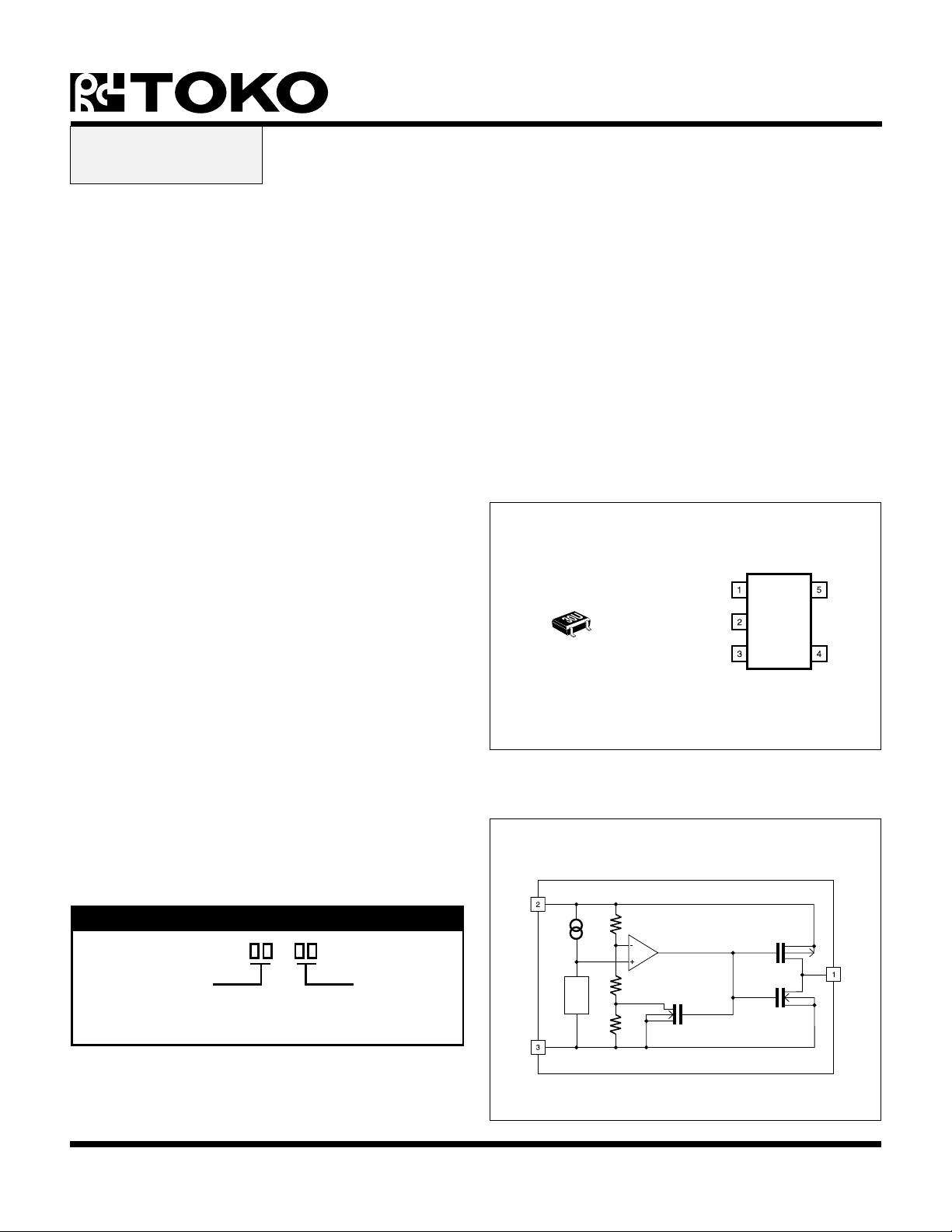
TK610xx
OUT
V
DD
GND
NC
NC
The TK610xx is available in a miniature SOT23-5 surface
mount package.
BLOCK DIAGRAM
V
DD
ORDERING INFORMATION
TK610 S
Voltage Code
VOLTAGE CODE *
23 = 2.3 V
25 = 2.5 V
27 = 2.7 V
30 = 3.0 V
33 = 3.3 V
* Consult factory for availability of other voltages
36 = 3.6 V
40 = 4.0 V
41 = 4.1 V
42 = 4.2 V
45 = 4.5 V
Tape/Reel Code
TAPE/REEL CODE
TL: Tape Left
GND
V
ref
October 1999 TOKO, Inc. Page 1
OUT

TK610xx
ABSOLUTE MAXIMUM RATINGS
All Pins Except GND ................................................ 11 V
Power Dissipation (Note 4) ................................ 400 mW
Storage Temperature Range ................... -40 to +125 °C
TK610xx ELECTRICAL CHARACTERISTICS
TA = 25 °C, unless otherwise specified.
LOBMYSRETEMARAPSNOITIDNOCTSETNIMPYTXAMSTINU
Operating Temperature Range ...................-30 to +80 °C
Junction Temperature ...........................................150 °C
V
RRE
ycaruccAegatloV1etoN2-2+%
SYHsiseretsyH2etoN 357%
V
HDD
V
LDD
∆V
TED
V
* ∆T
TED
t
RD
I
LSS
I
MSS
I
HSS
I
1NO
I
2NO
I
1PO
egatloVnoitceteD
)L(tnerruCylppuSV
)M(tnerruCylppuS
)H(tnerruCylppuS
egatloVgnitarepOmumixaM9V
egatloVgnitarepOtsewoL 8.0V
tneiciffeoCerutarepmeT
C°03- ≤ pot ≤ C°08001±C°/mpp
emiTyaleDnoitagaporPesiR3etoN001cesµ
DD
V
DD
V
DD
)5etoN()1N(tnerruCtuptuOV
SD
)5etoN()2N(tnerruCtuptuOV
SD
V
SD
)6etoN()1P(tnerruCtuptuO
V0.1=0.1Aµ
,V0.5=
V0.2 ≤ egatloVgnitteS ≤ V0.5
,V0.7=
V2.4 ≤ egatloVgnitteS ≤ V0.5
V,V50.0=
DD
V,V5.0=
DD
V,V1.2=
DD
V8.0=10.050.0Am
V5.1=0.20.4Am
,V5.4=
V0.2 ≤ egatloVgnitteS ≤ V1.4
0.20.4Am
0.10.2Aµ
5.10.3Aµ
V
SD
I
1PO
Note 1: V
Note 2: HYS = 100 * (V
Note 3: The applied voltage is a pulse of V
Note 4: Power dissipation is 400 mW when mounted as recommended. Derate at 3.2 mW/°C for operation above 25 °C.
Power dissipation is 200 mW in Free Air. Derate at 1.6 mW/°C for operation above 25 °C.
Note 5: Output sink current.
Note 6: Output source current.
= 100 * (V
ERR
- Setting Voltage) / Setting Voltage expressed in %
DET
- V
) / V
HYS
DET
expressed in %
DET
LOW
)6etoN()1P(tnerruCtuptuO
= 0.8 V, V
V2.4 ≤ egatloVgnitteS ≤ V0.5
= V
HIGH
DET
+ 2 V
V,V1.2=
DD
,V0.7=
0.60.8Am
Page 2 October 1999 TOKO, Inc.

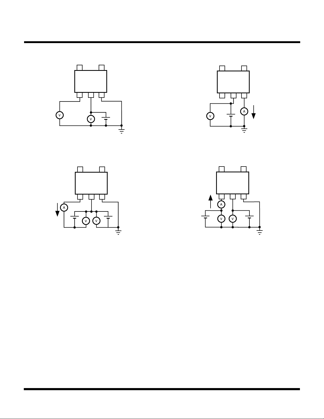
TEST CIRCUIT
TK610xx
OUT VDDGND
FIGURE 1: TEST CIRCUIT FOR V
V
, t
DDL
DR
OUT VDDGND
OV
V
DS
G
V
DD
V
DD
DET
, V
HYS
, V
DDH
OUT VDDGND
V
DD
,
FIGURE 3: TEST CIRCUIT FOR I
OUT VDDGND
OV
V
DS
G
V
DD
SS
FIGURE 2: TEST CIRCUIT FOR I
OP
FIGURE 4: TEST CIRCUIT FOR I
ON
October 1999 TOKO, Inc. Page 3
 Loading...