TOKO TK15410MTL Datasheet

TK15410
75 Ω VIDEO LINE DRIVER
FEATURES
■ Superimpose Circuit for Character (140 IRE) and
Border (70 IRE) Generation
■ Fixed Gain (6 dB)
■ Internal 75 Ω Driver with Clamp Circuit
■ Very Small Output Capacitor Using SAG Function Pin
■ Active High ON/OFF Control
■ Very Low Standby Current (typ. I
≤ 25 µA)
STBY
■ Single +5 V Power Supply Operation
DESCRIPTION
Operating from a single +5 V supply, the TK15410 is a
single-channel video line driver IC that takes a standard
video analog input and provides a buffered analog output
for driving a 150 Ω load. The standard video input signal
(1 V
typical) is internally clamped to 1.25 V and amplified
P-P
6 dB to produce 2 V
and 75 Ω cable load. The internal 1.5 k SAG function
resistor provides gain compensation for low frequency
signals. The built-in superimpose circuit provides the
addition of character (140 IRE) and border (70 IRE)
generation to the video signal. During standby (Pin 5
grounded), the TK15410 consumes only 125 µW of power.
Nominal power dissipation (no input) is typically 73 mW.
(typical) into a series 75 Ω resistor
P-P
APPLICATIONS
■ Video Equipment
■ Digital Cameras
■ CCD Cameras
■ TV Monitors
■ Video Tape Recorders
■ LCD Projectors
TK15410
INPUT
01S
CHARACTER
INPUT
BORDER
INPUT
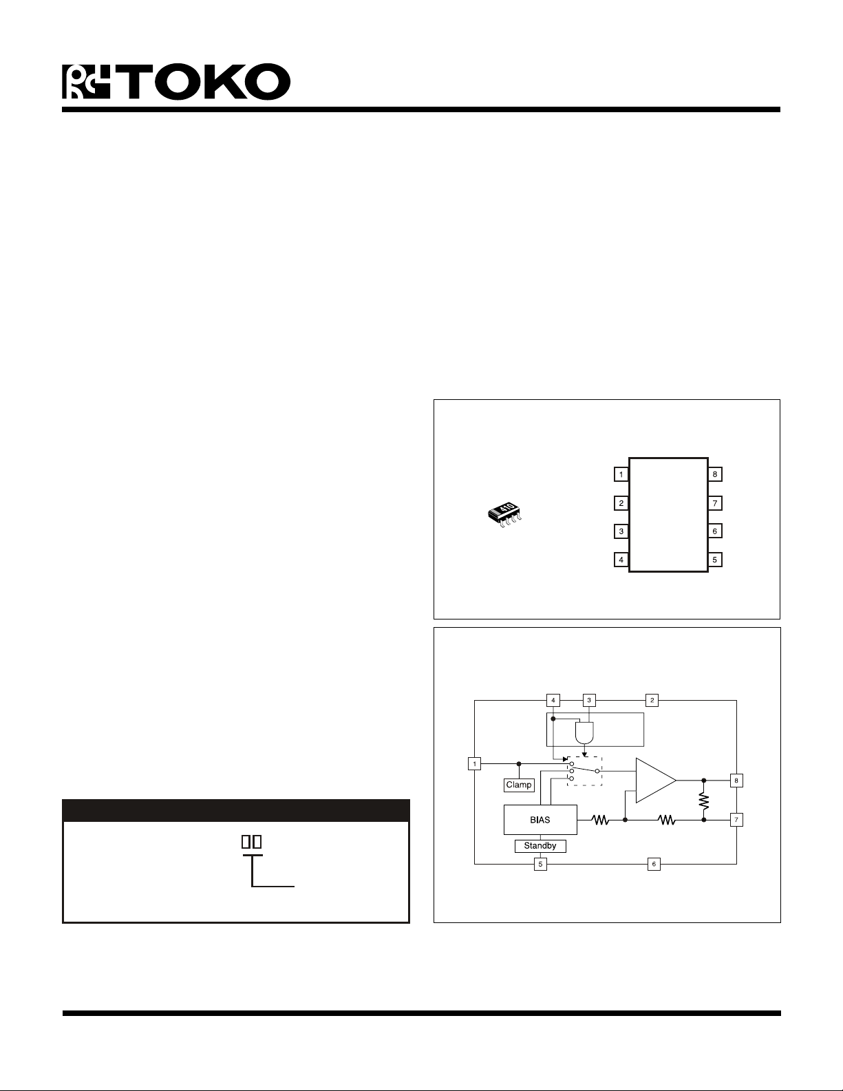
BLOCK DIAGRAM
OUTPUT
V
CC
SAG
GND
STANDBY
The TK15410M is available in the SOT23L-8 surface
mount package.
Logic
V
CC
Driver
75 Ω
1.5 kΩ
ORDERING INFORMATION
5 kΩ 5 kΩ
TK15410M
Tape/Reel Code
TAPE/REEL CODE
TL: Tape Left
January 2000 TOKO, Inc. Page 1
GND

TK15410
ABSOLUTE MAXIMUM RATINGS
Supply Voltage ........................................................... 6 V
Operating Voltage Range.............................. 4.5 to 5.5 V
Storage Temperature Range ................... -55 to +150 °C
Operating Temperature Range ...................-25 to +85 °C
Power Dissipation (Note 1) ................................ 200 mW
TK15410M ELECTRICAL CHARACTERISTICS
Test conditions: V
LOBMYSRETEMARAPSNOITIDNOCTSETNIMPYTXAMSTINU
I
CC
I
YBTS
I
SO
V
V
V
V
)REPUS(LHT
)REPUS(HLT
)YBTS(LHT
)YBTS*HLT
= 5.0 V, VIN = 1.0 V
CC
tnerruCylppuStupnioN5.410.02Am
)woLothgiH(
)hgiHotwoL(
, RL = 150 Ω, TA = 25 °C unless otherwise specified.
P-P
tnerruCylppuSybdnatSdednuorG5niP0.520.05Aµ
tnerruClanimreTybdnatSedomybdnatSni5niP0.520.05Aµ
dlohserhTesopmirepuS
)woLothgiH(egatloV
dlohserhTesopmirepuS
)hgiHotwoL(egatloV
4niP,3niPDNG08.0V
4niP,3niP00.2V
egatloVdlohserhTybdnatS
edom
egatloVdlohserhTybdnatS
edom
CC
ybdnatSotgnitarepO5niP
gnitarepOotybdnatS5niP
DNG06.0V
00.2V
CC
V
V
V
PMC
V
AHC
V
ROB
AVGniaGegatloVf
egatloVpmalClanimrettupnI1niP50.152.154.1V
leveLretcarahClanimretGAS7niP031041051ERI
leveLredroBlanimretGAS7niP060708ERI
ni
zHM1=54.559.554.6Bd
GDniaGlaitnereffiDtupnilangisesacriatS0.3-3.1+0.3+%
PDesahPlaitnereffiDtupnilangisesacriatS0.3-2.0+0.3+ged
rfesnopseRycneuqerFf
Note 1: Power dissipation is 200 mW in free air. Derate at 1.6 mW/°C for operation above 25°C.
ni
zHM5/zHM1=4.0-Bd
Page 2 January 2000 TOKO, Inc.

TEST CIRCUIT
TP5 TP4
VCC = 5.0 V
TK15410
V
CC
+
33 µF
TP1
Input
75 Ω
4.7 µF
+
+
33 µF
+
33 µF
V
OUT
Output
= 2.0 V
75 Ω
P-P
TP2
TP3
75 Ω
Output Truth Table
3niP4niPtuptuO
LL 1niP
LHV
ROB
HL 1niP
HH V
AHC
MEASUREMENT METHOD
1. Supply Current (ICC)
The Pin 2 current is measured with no input signal and the Standby Pin (Pin 5) open.
2. Standby Supply Current (I
STBY
)
The Pin 2 current is measured when the Standby Pin (Pin 5) is connected to ground.
3. Standby Terminal Current (IOS)
The Pin 5 current is measured when the Standby Pin (Pin 5) is connected to ground.
4. Standby Threshold Voltage (High to Low) (V
THL(STBY)
)
The Pin 5 voltage is measured at the point which changes the device from operating mode into standby mode.
January 2000 TOKO, Inc. Page 3
 Loading...