TOKO TK15409MTL Datasheet

TK15409
75 Ω VIDEO LINE DRIVER
FEATURES
■ Internal Y-C Summing Circuit
■ Voltage Gain is 6 dB Fixed
■ Internal 75
Ω Driver
■ Active High ON/OFF Control
■ Very Low Standby Current (typ. I
≤ 25 µA)
STBY
■ Very Small Output Capacitor Using SAG Function Pin
■ Very Small Package (SOT23L-8)
■ Single +5 V Power Supply Operation
DESCRIPTION
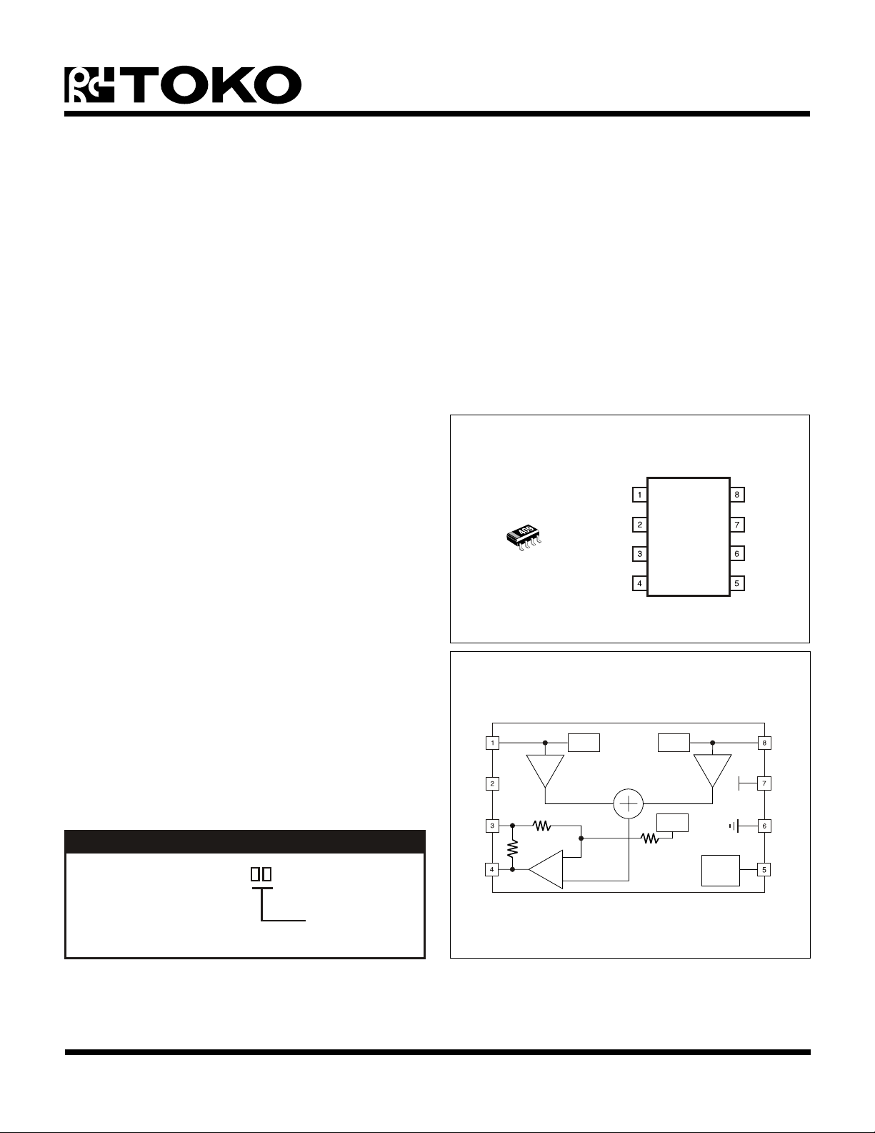
Operating from a single +5 V supply, the TK15409 is a
video line driver IC that takes standard Y and C analog
inputs and provides a composite analog output for driving
150 Ω loads (75 Ω resistor and 75 Ω cable load). Internal
summing of the Y and C inputs is performed to produce the
composite video output. The luminance (Y) input is
clamped at 1.25 V and amplified 6 dB; the chromanance
(C) input is biased at 2.0 V and amplified 6 dB. The internal
1.5 kΩ SAG function resistor provides gain compensation
for low frequency signals. During standby (Pin 5 grounded),
the TK15409 consumes only 127 µW of power. Nominal
power dissipation (no input) is typically 90 mW.
The TK15409M is available in the very small SOT23L-8
surface mount package.
APPLICATIONS
■ Video Equipment
■ Digital Cameras
■ CCD Cameras
■ TV Monitors
■ Video Tape Recorders
■ LCD Projectors
TK15409
Y-INPUT
01S
OUTPUT
BLOCK DIAGRAM
N/C
SAG
C-INPUT
V
CC
GND
STANDBY
ORDERING INFORMATION
TK15409M
Tape/Reel Code
TAPE/REEL CODE
TL: Tape Left
5 kΩ
1.5 kΩ
6 dB
Amp
6 dB
75 Ω
DRIVER
Clamp
1.25 V
5 kΩ
BIAS
2.0 V
Clamp
1.25 V
6 dB
Amp
Reference
&
Standby
CC
V
January 2000 TOKO, Inc. Page 1

TK15409
ABSOLUTE MAXIMUM RATINGS
Supply Voltage ........................................................... 6 V
Operating Voltage Range.............................. 4.5 to 5.5 V
Power Dissipation (Note 1) ................................ 350 mW
Input Frequency ............................................... 10.0 MHz
Storage Temperature Range ................... -55 to +150 °C
Operating Temperature Range ...................-25 to +85 °C
TK15409M ELECTRICAL CHARACTERISTICS
Test conditions: V
LOBMYSRETEMARAPSNOITIDNOCTSETNIMPYTXAMSTINU
I
CC
I
YBTS
I
SO
V
LHT
V
HLT
V
PMC
V
SAIB
1Y-AVG1-hcYniaGegatloVf
2Y-AVG2-hcYniaGegatloVf
1C-AVG1-hcCniaGegatloVf
2C-AVG1-hcCniaGegatloVf
GDniaGlaitnereffiDtupnilangisesacriatS0.3-2.1-0.3+%
= 5.0 V, VIN = 1.0 V
CC
tnerruCylppuStupnioN0.810.62Am
)woL
)hgiH
egatloVpmalClanimrettupnilangisY1niP01.182.105.1V
egatloVsaiBlanimrettupnilangisC8niP07.100.203.2V
, RL = 150 Ω, TA = 25 °C unless otherwise specified.
P-P
tnerruCylppuSybdnatSdednuorG5niP3.520.05Aµ
tnerruClanimreTybdnatSedomybdnatSni5niP3.520.05Aµ
othgiH(egatloVdlohserhT
edom
otwoL(egatloVdlohserhT
edom
NI
NI
NI
NI
ybdnatSotgnitarepO5niP
gnitarepOotybdnatS5niP
DNG3.0V
8.1V
CC
tupnilangisY,zHM1=2.57.52.6Bd
tupnilangisY,zHk51=2.57.52.6Bd
tupnilangisC,zHM1=1.56.51.6Bd
tupnilangisC,zHk51=1.56.51.6Bd
V
PDesahPlaitnereffiDtupnilangisesacriatS0.3-4.0-0.3+ged
rfesnopseRycneuqerFf
Note 1: Power dissipation is 350 mW in free air. Derate at 2.8 mW/°C for operation above 25°C.
ni
zHM5/zHM1=5.0-Bd
Page 2 January 2000 TOKO, Inc.

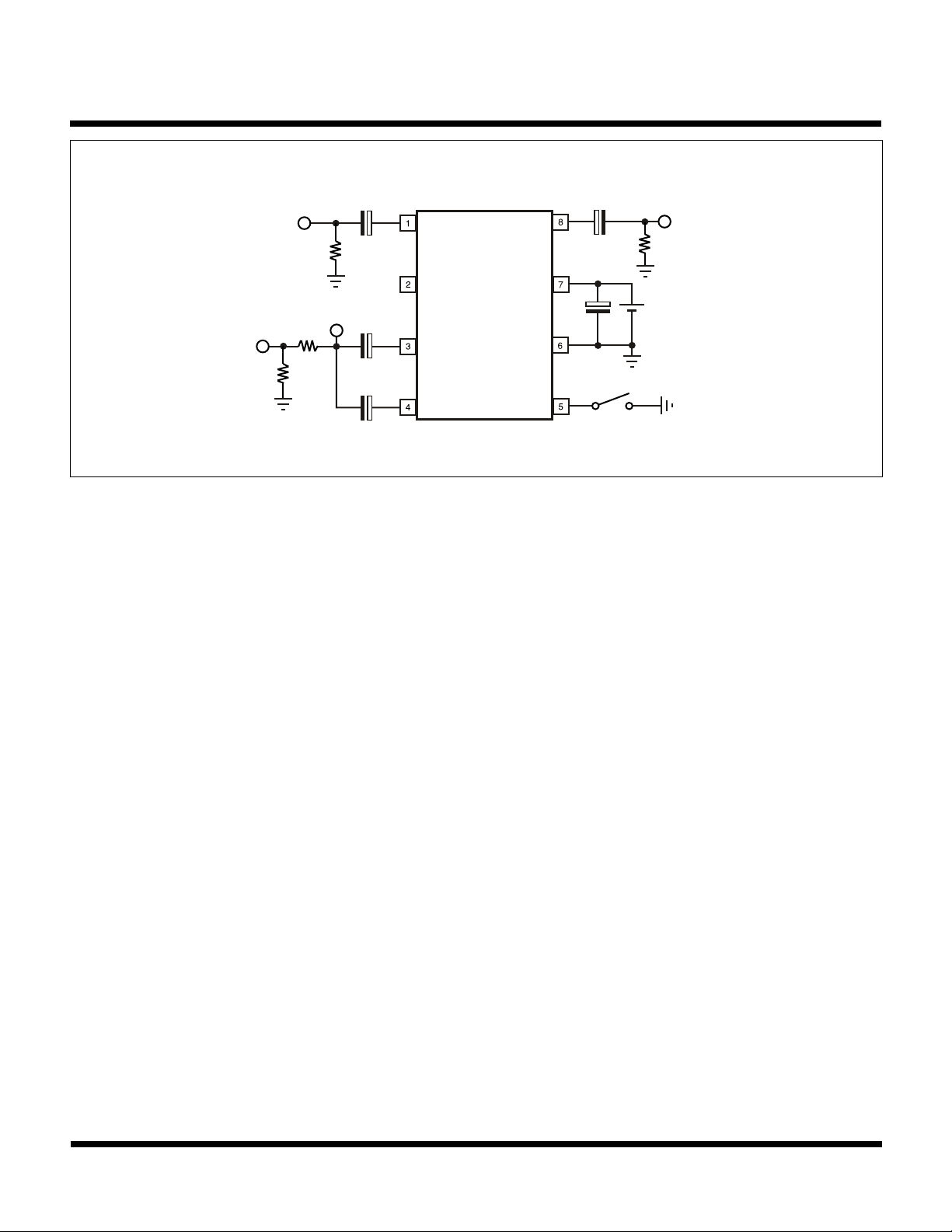
TEST CIRCUIT
TK15409
75 Ω
Y - INPUT
CVBS - OUTPUT
V
= 2.0 V
OUT
75 Ω
4.7 µF
75 Ω
P-P
33 µF
33 µF
OUTPUT
+
N/C
SAG
+
+
33 µF
4.7 µF
+
GND
Standby
C - INPUT
75 Ω
+
VCC = 5.0 V
January 2000 TOKO, Inc. Page 3
 Loading...