TOKO TK15408MTL Datasheet

TK15408
75 Ω VIDEO LINE DRIVER
FEATURES
■ Fixed Gain (6 dB)
■ Internal 75 Ω Drivers
■ Very Small Output Capacitor Using SAG Function Pin
■ Internal Clamping Circuit
■ Single +5 V Power Supply Operation
DESCRIPTION
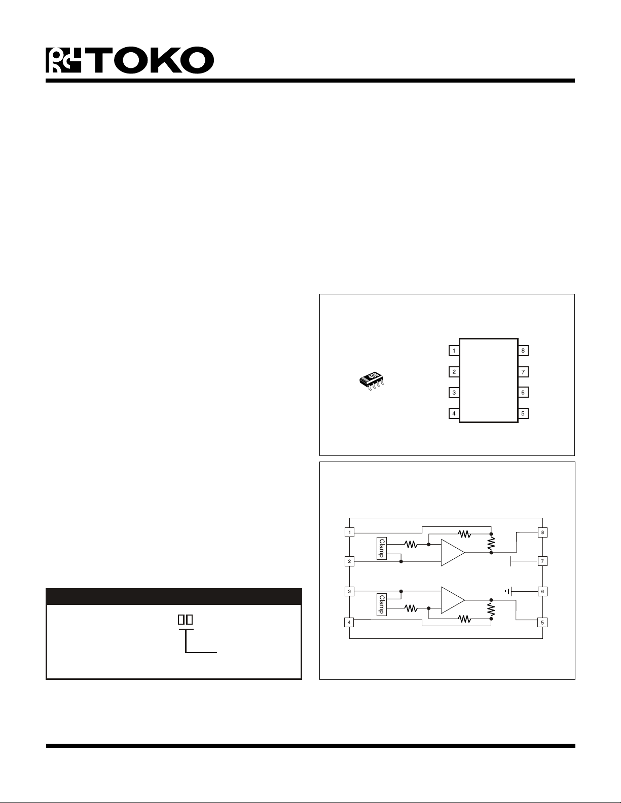
Operating from a single +5 V supply, the TK15408 is a dual
video driver IC that takes standard video signals as analog
inputs and provides buffered analog outputs for driving
150 Ω loads (series 75 Ω resistor and 75 Ω cable load).
Both amplifiers have a fixed gain of 6 dB with internal
clamping circuits. Each input is clamped at 1.29 V and
amplified 6 dB to produce 2 V
75 Ω resistor and 75 Ω cable load. The internal 1.5 k SAG
function resistors provide gain compensation for low
frequency signals. Nominal power dissipation (no input) is
typically 76 mW. The TK15408 is ideally suited for S-VHS
systems.
The TK15408M is available in the very small SOT23L-8
surface mount package.
(typical) into a series
P-P
APPLICATIONS
■ Video Equipment
■ Digital Cameras
■ CCD Cameras
■ TV Monitors
■ Video Tape Recorders
■ LCD Projectors
TK15408
SAG_A
01S
INPUT_A
INPUT_B
SAG_B
BLOCK DIAGRAM
OUTPUT_A
V
CC
GND
OUTPUT_B
ORDERING INFORMATION
TK15408M
Tape/Reel Code
TAPE/REEL CODE
TL: Tape Left
5 kΩ
5 kΩ
5 kΩ
-
Driver
75 Ω
+
+
Driver
75 Ω
-
5 kΩ 1.5 kΩ
1.5 kΩ
V
CC
December 1999 TOKO, Inc. Page 1

TK15408
ABSOLUTE MAXIMUM RATINGS
Supply Voltage ........................................................... 6 V
Operating Voltage Range.............................. 4.5 to 5.5 V
Storage Temperature Range ................... -55 to +150 °C
Operating Temperature Range ...................-25 to +75 °C
Power Dissipation (Note 1) ................................ 200 mW
TK15408M ELECTRICAL CHARACTERISTICS
Test conditions: V
LOBMYSRETEMARAPSNOITIDNOCTSETNIMPYTXAMSTINU
I
CC
V
PMC
AVGniaGegatloVf
GDniaGlaitnereffiDtupnilangisesacriatS0.3-6.0+0.3+%
PDesahPlaitnereffiDtupnilangisesacriatS0.3-1.0-0.3+ged
rfesnopseRycneuqerFf
Note 1: Power dissipation is 200 mW in free air. Derate at 1.6 mW/°C for operation above 25°C.
= 5.0 V, VIN = 1.0 V
CC
tnerruCylppuStupnioN1.510.12Am
egatloVpmalClanimrettupnI3niP,2niP01.192.105.1V
, RL = 150 Ω, TA = 25 °C unless otherwise specified.
P-P
ni
ni
zHM1=2.57.52.6Bd
zHM5/zHM1=3.0-Bd
Page 2 December 1999 TOKO, Inc.

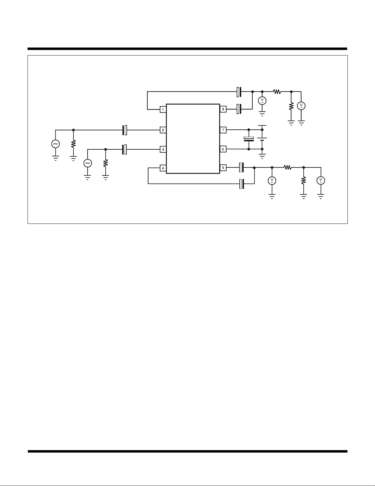
TEST CIRCUIT
TK15408
SAG_A
TP1
75 Ω
4.7 µF
TP4
4.7 µF
75 Ω
INPUT_A
+
INPUT_B
+
SAG_B
MEASUREMENT METHOD
1. Supply Current (ICC)
The Pin 7 current is measured with no input signal.
33 µF
OUTPUT_A
V
CC
33 µF
GND
OUTPUT B
++
33 µF
33 µF
+
+
33 µF
75 Ω
TP2
V
CC
+
5.0 V
TP5
75 Ω
75 Ω
TP3
TP6
75 Ω
2. Clamp Voltage (V
CMP
)
The DC voltage at Pin 2 (Pin 3) is measured with no input signal.
3. Voltage Gain (GVA)
The voltage gain equation is as follows:
GVA = 20 log10 V2/V1
Where V1 is the input voltage at TP1 (TP4) and V2 is the measured voltage at TP2 (TP5).
4. Differential Gain (DG)
The differential gain is measured at TP3 (TP6) when a staircase waveform of 10 steps is applied to TP1 (TP4).
5. Differential Phase (DP)
The differential phase is measured at TP3 (TP6) when a staircase waveform of 10 steps is applied to TP1 (TP4).
6. Frequency Response (fr)
The frequency response equation is as follows:
fr = 20 log10 V2/V1
Where V1 is the measured TP3 (TP6) voltage when the TP1 (TP4) input frequency is set to 1 MHz and V2 is the measured
TP3 (TP6) voltage when the TP1 (TP4) input frequency is set to 5 MHz.
December 1999 TOKO, Inc. Page 3
 Loading...