TOKO TK15407MTL Datasheet

TK15407
75 Ω VIDEO LINE DRIVER
FEATURES
■ Fixed Gain (6 dB)
■ Internal 75 Ω Drivers
■ Very Small Output Capacitor Using SAG Function Pin
■ Active High ON/OFF Control
■ Very Low Standby Current (typ. I
≤ 25 µA)
STBY
■ Very Small SOT23L-8 Package
DESCRIPTION
Operating from a single +5 V supply, the TK15407 is a dual
video driver IC that takes standard video signals as analog
inputs and provides buffered analog outputs for driving
150 Ω loads (series 75 Ω resistor and 75 Ω cable load).
Both amplifiers have a fixed gain of 6 dB and can be used
in series for 12 dB gain. The luminance (Y) input is
clamped at 1.29 V and amplified 6 dB to produce 2 V
(typical) into a series 75 Ω resistor and 75 Ω cable load.
The internal 1.5 k SAG function resistor provides gain
compensation for low frequency signals. The chromanance
(C) input is biased at 2.6 V and amplified 6 dB to produce
1.1 V
(typical) into a series 75 Ω resistor and 75 Ω cable
P-P
load. During standby (Pin 3 grounded), the TK15407
consumes only 119 µW of power. Nominal power
dissipation (no input) is typically 76 mW. The TK15407 is
ideally suited for S-VHS systems.
The TK15407M is available in the very small SOT23L-8
surface mount package.
P-P
APPLICATIONS
■ Video Equipment
■ Digital Cameras
■ CCD Cameras
■ TV Monitors
■ Video Tape Recorders
■ LCD Projectors
TK15407
SAG_Y
INPUT_Y
01S
STANDBY
INPUT_C
BLOCK DIAGRAM
5 kΩ
OUTPUT_Y
V
CC
GND
OUTPUT_C
5 kΩ
-
+
1.5 kΩ
V
CC
ORDERING INFORMATION
TK15407M
Tape/Reel Code
TAPE/REEL CODE
TL: Tape Left
100 kΩ
5 kΩ
+
-
5 kΩ
January 2000 TOKO, Inc. Page 1

TK15407
ABSOLUTE MAXIMUM RATINGS
Supply Voltage ........................................................... 6 V
Operating Voltage Range.............................. 4.5 to 5.5 V
Storage Temperature Range ................... -55 to +150 °C
Operating Temperature Range ...................-25 to +75 °C
Power Dissipation (Note 1) ................................ 200 mW
TK15407M ELECTRICAL CHARACTERISTICS
Test conditions: V
LOBMYSRETEMARAPSNOITIDNOCTSETNIMPYTXAMSTINU
I
CC
I
YBTS
I
SO
V
LHT
V
HLT
V
PMC
V
SAIB
AVGniaGegatloVf
GD)langiSY(niaGlaitnereffiDtupnilangisesacriatS0.3-3.1+0.3+%
= 5.0 V, VIN = 1.0 V
CC
tnerruCylppuStupnioN1.510.12Am
)woL
)hgiH
egatloVpmalClanimrettupnIlangiSY2niP01.192.105.1V
egatloVsaiBlanimrettupnIlangiSC4niP53.266.259.2V
, RL = 150 Ω, TA = 25 °C unless otherwise specified.
P-P
tnerruCylppuSybdnatSdednuorG3niP8.320.05Aµ
tnerruClanimreTybdnatSedomybdnatSni3niP8.320.05Aµ
othgiH(egatloVdlohserhT
edom
otwoL(egatloVdlohserhT
edom
ni
zHM1=2.57.52.6Bd
ybdnatSotgnitarepO3niP
gnitarepOotybdnatS3niP
DNG1.03.0V
8.10.2VCCV
PD)langiSY(esahPlaitnereffiDtupnilangisesacriatS0.3-0.00.3+ged
rfesnopseRycneuqerFf
DHT
V
Note 1: Power dissipation is 200 mW in free air. Derate at 1.6 mW/°C for operation above 25°C.
)XAM(TUO
)langiSC(
)langiSC(
noitrotsiDcinomraHlatoT
egatloVtuptuOmumixaM
ni
f
ni
zHk0.1=4.05.1%
zHM5/zHM1=3.0-Bd
tniop%01=DHT9.01.1smrV
Page 2 January 2000 TOKO, Inc.

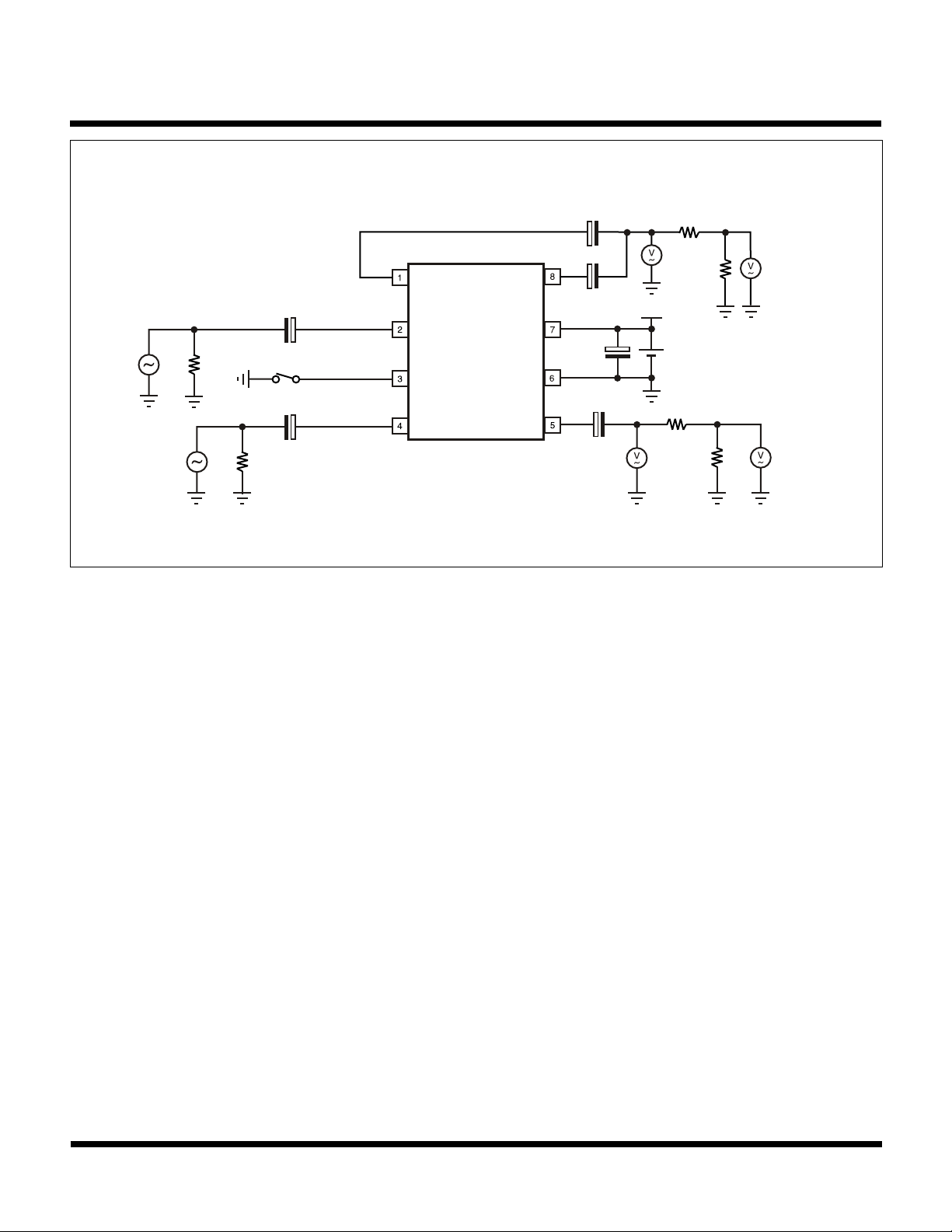
TEST CIRCUIT
TK15407
33 µF
++
33 µF
TP1
+
4.7 µF
75 Ω
TP4
+
4.7 µF
75 Ω
33 µF
+
+
33 µF
TP5 TP6
MEASUREMENT METHOD
1. Supply Current (ICC)
The Pin 7 current is measured with no input signal and the Standby Pin (Pin 3) open.
TP2
V
CC
5.0 V
75 Ω
75 Ω
TP3
75 Ω
75 Ω
2. Standby Supply Current (I
The Pin 7 current is measured when the Standby Pin (Pin 3 ) is connected to ground.
STBY
)
3. Standby Terminal Current (IOS)
The Pin 3 current is measured when Pin 3 is connected to ground.
4. Threshold Voltage (High to Low) (V
The Pin 3 voltage is measured at the point which changes the device from operating mode into standby mode.
5. Threshold Voltage (Low to High) (V
The Pin 3 voltage is measured at the point which changes the device from standby mode into operating mode.
6. Clamp Voltage (V
The DC voltage at Pin 2 is measured with no input signal.
7. Bias Voltage (V
The DC voltage at Pin 4 is measured with no input signal.
BIAS
CMP
)
)
THL
TLH
)
)
8. Voltage Gain (GVA)
The voltage gain equation is as follows:
GVA = 20 log10 V2/V1
Where V1 is the input voltage at TP1 (TP4) and V2 is the measured voltage at TP2 (TP5).
9. Differential Gain (DG)
The differential gain is measured at TP3 when a staircase waveform of 10 steps is applied to TP1.
January 2000 TOKO, Inc. Page 3
 Loading...