TOKO TK15406MTL Datasheet

TK15406
75 Ω VIDEO LINE DRIVER
FEATURES
■ Internal 75 Ω Driver
■ Active High ON/OFF Control with Internal Pull-up
■ Very Low Standby Current (typ. I
STBY
≤ 25 µA)
■ Very Small SOT23-6 Package
■ Single +5 V Power Supply Operation
DESCRIPTION
Operating from a single +5 V supply, the TK15406 is a
single-channel video line driver IC that takes a standard
video analog input and provides a buffered analog output
for driving a 150 Ω load. The standard video input signal
(1 V
6 dB to produce 2 V
and 75 Ω cable load. During standby (Pin 1 grounded), the
TK15406 consumes only 120 µW of power. Nominal
power dissipation (no input) is typically 32 mW.
typical) is internally biased at 2.5 V and amplified
P-P
(typical) into a series 75 Ω resistor
P-P
APPLICATIONS
■ Video Equipment
■ Digital Cameras
■ CCD Cameras
■ TV Monitors
■ Video Tape Recorders
■ LCD Projectors
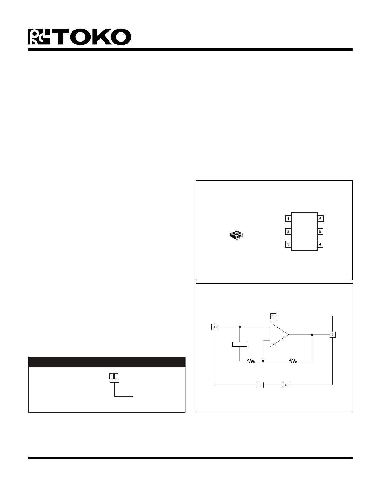
TK15406
STANDBY
1S
0
OUTPUT
N/C
V
CC
GND
INPUT
The TK15406M is available in the very small SOT23-6
surface mount package.
ORDERING INFORMATION
TK15406M
Tape/Reel Code
TAPE/REEL CODE
TL: Tape Left
BLOCK DIAGRAM
V
BIAS
5 kΩ 5 kΩ
STANDBY
CC
DRIVER
75 Ω
GND
January 2000 TOKO, Inc. Page 1

TK15406
TK15406M ABSOLUTE MAXIMUM RATINGS
Supply Voltage ........................................................... 6 V
Operating Voltage ......................................... 4.5 to 5.5 V
Storage Temperature Range ................... -55 to +150 °C
Operating Temperature Range ...................-25 to +75 °C
Power Dissipation (Note 1) ............................... 150 mW
TK15406M ELECTRICAL CHARACTERISTICS
Test conditions: V
LOBMYSRETEMARAPSNOITIDNOCTSETNIMPYTXAMSTINU
I
CC
I
YBTS
I
SO
V
LHT
V
HLT
V
SAIB
AVGniaGegatloVf
rfesnopseRycneuqerFf
DHTnoitrotsiDcinomraHlatoTf
V
Note 1: Power dissipation is 150 mW in free air. Derate at 1.2 mW/°C for operation above 25°C.
)XAM(TUO
= 5.0 V, VIN = 1.0 V
CC
, RL = 150 Ω, TA = 25 °C unless otherwise specified.
P-P
tnerruCylppuStupnioN3.65.8Am
tnerruCylppuSybdnatSdednuorG1niP0.420.05Aµ
tnerruClanimreTybdnatSedomybdnatSni1niP0.420.05Aµ
egatloVdlohserhTybdnatS
)woLothgiH(
edom
egatloVdlohserhTybdnatS
)hgiHotwoL(
edom
ybdnatSotgnitarepO1niP
gnitarepOotybdnatS1niP
egatloVsaiBlanimrettupnI4niP51.254.257.2V
ni
ni
ni
zHM1=2.57.52.6Bd
zHM5/zHM1=5.0-Bd
zHk0.1=2.00.1%
egatloVtuptuOmumixaMtniop%01=DHT0.12.1smrV
DNG1.03.0V
8.10.2VCCV
Page 2 January 2000 TOKO, Inc.

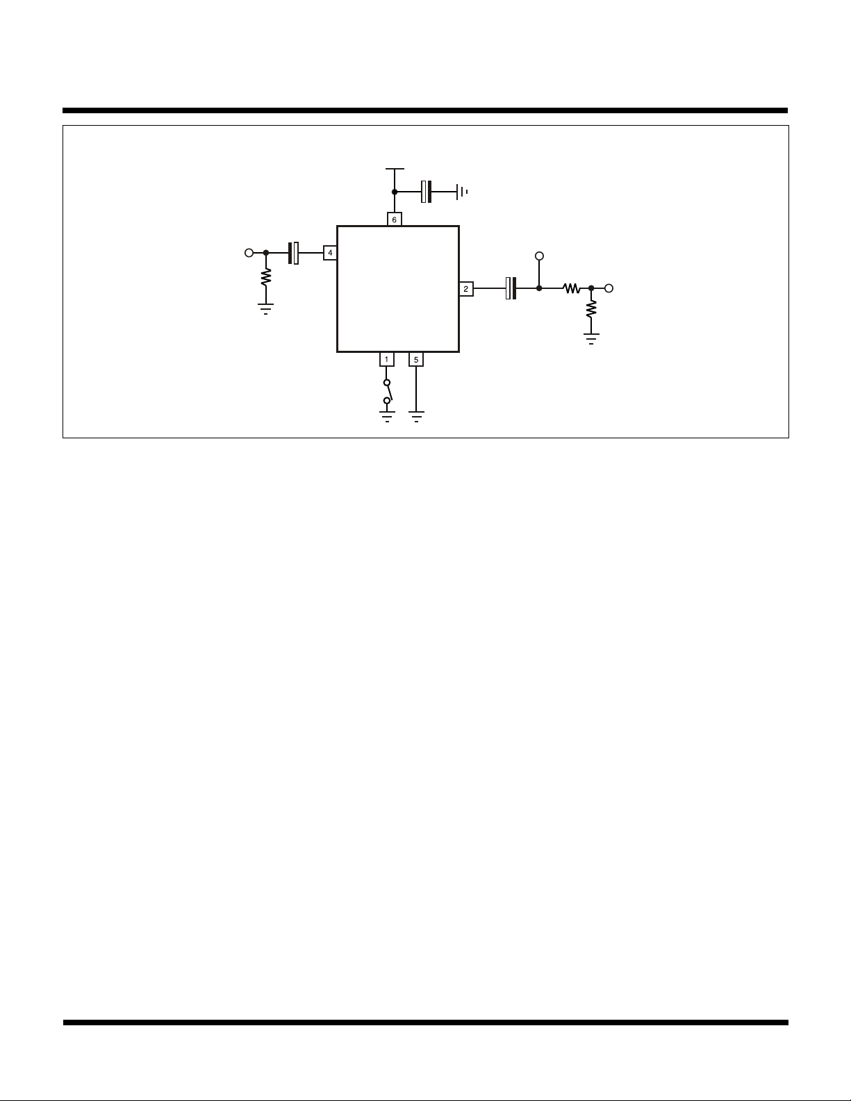
TEST CIRCUIT
V
CC
+
VCC = 5.0 V
33 µF
TK15406
+Input
TP1
75 Ω
4.7 µF
+
Standby GND
+
47 µF
TP2
V
OUT
Output
= 2.0 V
75 Ω
75 Ω
P-P
TP3
MEASUREMENT METHOD
1. Supply Current (ICC)
The Pin 6 current is measured with no input signal and the Standby Pin (Pin 1) open.
2. Standby Supply Current (I
The Pin 6 current is measured when the Standby Pin (Pin 1) is connected to ground.
STBY
)
3. Standby Terminal Current (IOS)
The Pin 1 current is measured when Pin 1 is connected to ground.
4. Threshold Voltage (High to Low) (V
The Pin 1 voltage is measured at the point which changes the device from operating mode into standby mode.
THL
)
5. Threshold Voltage (Low to High) (V
The Pin 1 voltage is measured at the point which changes the device from standby mode into operating mode.
6. Bias Voltage (V
The DC voltage at Pin 4 is measured with no input signal.
BIAS
)
TLH
)
7. Voltage Gain (GVA)
The voltage gain equation is as follows:
GVA = 20 log10 V2/V1
Where V1 is the input voltage at TP1 and V2 is the measured output voltage at TP2.
8. Frequency Response (fr)
The frequency response equation is as follows:
fr = 20 log10 V2/V1
Where V1 is the measured TP3 voltage when the TP1 input frequency is set to 1 MHz and V2 is the measured TP3 voltage
when the TP1 input frequency is set to 5 MHz.
9. Total Harmonic Distortion (THD)
The TP3 signal is measured when a 1 kHz 1 V
10. Maximum Output Voltage (V
A 1 kHz input signal is applied to TP1 and the amplitude is slowly increased. The output voltage at TP2 is measured at
OUT(MAX)
)
input signal is applied to TP1.
P-P
the point the THD reaches 10%.
January 2000 TOKO, Inc. Page 3
 Loading...