TOKO TK15403MTL Datasheet

TK15403
75 Ω VIDEO LINE DRIVER
FEATURES
■ Internal 75 Ω Drivers
■ 20 MHz Gain Band Width
■ 2 Channel High Speed Operational Amplifiers
■ Very Small SOT23L-8 Package
■ Single +5 V Power Supply Operation
DESCRIPTION
Operating from a single +5 V supply, the TK15403M is a
dual video line driver IC that takes standard video signals
as analog inputs and provides buffered analog outputs for
driving 150 Ω loads (series 75 Ω resistor and 75 Ω cable
load). The standard video input signals (1 V
typically amplified 6 dB using external components to
produce a 2 V
signal into an AC-coupled 150 Ω load.
P-P
Nominal power dissipation (no input) is typically 56 mW.
P-P
) are
APPLICATIONS
■ Video Equipment
■ Digital Cameras
■ CCD Cameras
■ TV Monitors
■ Video Tape Recorders
■ LCD Projectors
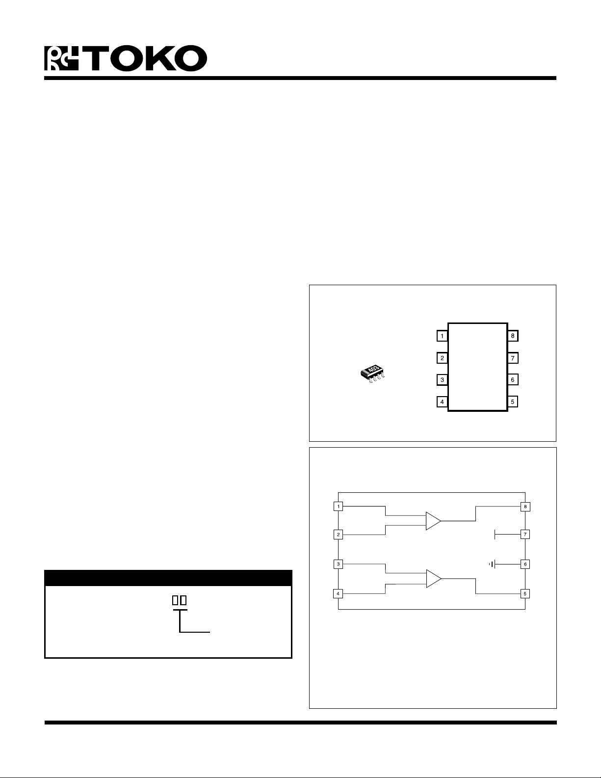
TK15403
01S
-INA
+INA
+INB
-INB
OUTA
V
CC
GND
OUTB
The TK15403M is available in the very small SOT23L-8
surface mount package.
ORDERING INFORMATION
TK15403M
Tape/Reel Code
TAPE/REEL CODE
TL: Tape Left
BLOCK DIAGRAM
+
+
-
CC
V
December 1999 TOKO, Inc. Page 1

TK15403
ABSOLUTE MAXIMUM RATINGS
Supply Voltage ........................................................... 6 V
Operating Voltage ......................................... 4.5 to 5.5 V
Storage Temperature Range ................... -55 to +150 °C
Operating Temperature Range ...................-25 to +75 °C
Power Dissipation (Note 1) ................................ 200 mW
TK15403M ELECTRICAL CHARACTERISTICS
Test conditions: V
LOBMYSRETEMARAPSNOITIDNOCTSETNIMPYTXAMSTINU
I
CC
AVGniaGegatloVf
1rf1esnopseRycneuqerFf
2rf2esnopseRycneuqerFf
DHTnoitrotsiDcinomraHlatoTf
V
)XAM(TUO
TCklaTssorCf
N/SoitaResioNotlangiSlangislatsedeP07-Bd
GDniaGlaitnereffiDtupnilangisesacriatS0.3-0.3+%
PDesahPlaitnereffiDtupnilangisesacriatS0.3-0.3+ged
= 5.0 V, VIN = 1.0 V
CC
tnerruCylppuStupnioN1.110.61Am
, RL = 150 Ω, TA = 25 °C unless otherwise specified.
P-P
ni
ni
ni
ni
zHk0.1=2.00.1%
)2etoN(zHM1=7.50.63.6Bd
zHM5/zHM1=4.0Bd
zHM01/zHM1=2.1-Bd
egatloVtuptuOmumixaMtniop%01=DHT0.12.1smrV
ni
zHM1=75-04-Bd
OVGniaGegatloVtiucriCnepO 04Bd
WBhtdiWdnaBycneuqerF 02zHM
RSetaRwelS 07Sµ/V
C
NI
R
NI
Note 1: Power dissipation is 200 mW in free air. Derate at 1.6 mW/°C for operation above 25°C.
Note 2: Set by external components.
ecnaticapaCtupnI 9Fp
ecnatsiseRtupnI 6.1MΩ
Page 2 December 1999 TOKO, Inc.

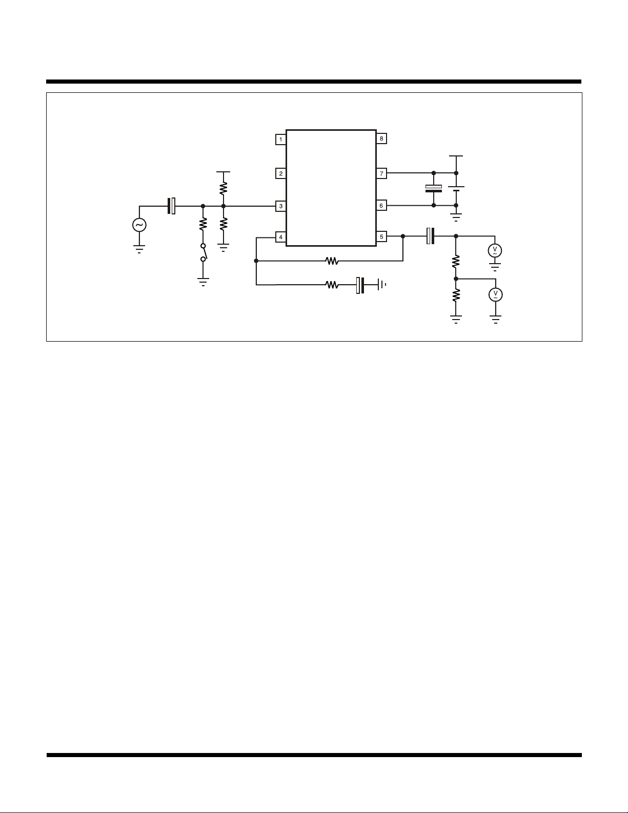
Channel A is the same measurement
circuit as Channel B.
4.7 µF
TP1
+
TK15403
TEST CIRCUIT
V
CC
V
CC
10 kΩ
33 µF
+
5 V
47 µF
+
75 Ω
75 Ω
SW1 is closed only
when DG and DP
are measured.
SW1
10 kΩ20 kΩ
47 µF
2 kΩ
+
2 kΩ
MEASUREMENT METHOD
1. Supply Current (ICC)
The Pin 7 current is measured with no input signal.
2. Voltage Gain (GVA)
The Voltage Gain equation is as follows:
GVA = 20 log10 V2/V1
Where V1 is the input voltage at TP1 and V2 is the measured voltage at TP2.
3. Frequency Response (fr1 and fr2)
The frequency response equation is as follows:
fr = 20 log10 V2/V1
Where V1 is the measured TP3 voltage when the TP1 input frequency is set to 1 MHz.
For fr1 V2 is the measured TP3 voltage when the TP1 input frequency is set to 5 MHz.
For fr2 V2 is the measured TP3 voltage when the TP1 input frequency is set to 10 MHz.
These measurements and calculations are taken for both channels.
TP2
TP3
4. Total Harmonic Distortion (THD)
The TP3 signal is measured when a 1 kHz 1 V
5. Maximum Output Voltage (V
OUT(MAX)
)
input signal is applied to TP1.
P-P
A 1 kHz input signal is applied to TP1 and slowly increased. The output voltage at TP2 is measured at the point the THD
reaches 10%.
6. Cross Talk (CT)
The Cross Talk equation is as follows:
CT = 20 log10 V1/V2
V1 is measured at output B when a 1 MHz input frequency and 1 V
measured at Output B when a 1 MHz input frequency and 1 V
P-P
input signal voltage is applied to Input A, V2 is
P-P
input signal voltage is applied to Input B.
CT is also calculated at the opposite side when V1 is measured at Output A when input signal is applied to Input B and
V2 is measured at Output A when input signal is applied to Input A.
December 1999 TOKO, Inc. Page 3
 Loading...