TOKO TK15402MTL Datasheet

TK15402
75 Ω VIDEO LINE DRIVER
FEATURES
■ Gain Set by External Components (6 dB typ.)
■ Internal 75 Ω Drivers
■ Active High ON/OFF Control
■ Very Low Standby Current (typ. I
≤ 25 µA)
STBY
■ Single +5 V Power Supply Operation
DESCRIPTION
Operating from a single +5 V supply, the TK15402 is a
triple video driver IC that takes standard video signals as
analog inputs and provides buffered analog outputs for
driving 150 Ω loads (series 75 Ω resistor and 75 Ω cable
load). The standard video input signals (1 V
typically amplified 6 dB using external components to
produce a 2 V
signal into an AC-coupled 150 Ω load.
P-P
During standby (Pin 2 grounded), the TK15402 consumes
only 113 µW of power. Nominal power dissipation (no
input) is typically 98 mW.
P-P
) are
APPLICATIONS
■ RGB Video Line Driver Applications
■ Video Equipment
■ Digital Cameras
■ CCD Cameras
■ TV Monitors
■ Video Tape Recorders
■ LCD Projectors
TK15402
V
CC
STANDBY
+INPUT 1
-INPUT 1
OUTPUT 1
GND
+INPUT 3
-INPUT 3
OUTPUT 3
OUTPUT 2
-INPUT 2
+INPUT 2
The TK15402M is available in the SSOP-12 Surface
Mount Package.
BLOCK DIAGRAM
V
CC
DRIVER
75 Ω
DRIVER
75 Ω
ORDERING INFORMATION
TK15402M
DRIVER
75 Ω
Tape/Reel Code
STANDBY
TAPE/REEL CODE
TL: Tape Left
January 2000 TOKO, Inc. Page 1
GND

TK15402
ABSOLUTE MAXIMUM RATINGS
Supply Voltage ........................................................... 6 V
Operating Voltage ......................................... 4.5 to 5.5 V
Storage Temperature Range ................... -55 to +150 °C
Operating Temperature Range ...................-25 to +75 °C
Power Dissipation (Note 1) ................................ 350 mW
TK15402M ELECTRICAL CHARACTERISTICS
Test conditions: V
LOBMYSRETEMARAPSNOITIDNOCTSETNIMPYTXAMSTINU
I
CC
I
YBTS
I
SO
V
LHT
V
HLT
AVGniaGegatloVf
rfesnopseRycneuqerF
DHTnoitrotsiDcinomraHlatoTf
V
)XAM(TUO
TCklaTssorCf
N/SoitaResioNotlangiSlangislatsedeP07-Bd
= 5.0 V, VIN = 1.0 V
CC
tnerruCylppuStupnioN5.910.72Am
)woL
)hgiH
, RL = 150 Ω, TA = 25 °C unless otherwise specified.
P-P
tnerruCylppuSybdnatSdednuorG2niP5.220.05Aµ
tnerruClanimreTybdnatSedomybdnatS2niP5.220.05Aµ
othgiH(egatloVdlohserhT
edom
otwoL(egatloVdlohserhT
edom
ni
f
ni
f
ni
NI
zHk0.1=2.00.1%
zHM5/zHM1=1.0-Bd
ybdnatSotgnitarepO2niP
gnitarepOotybdnatS2niP
DNG1.03.0V
8.10.2V
CC
)2etoN(zHM1=7.50.63.6Bd
zHM01/zHM1=1.1-Bd
egatloVtuptuOmumixaMtniop%01=DHT0.12.1smrV
ni
zHM1=55-04-Bd
V
GDniaGlaitnereffiDtupnievawesacriatS0.3-0.3+%
PDesahPlaitnereffiDtupnievawesacriatS0.3-0.3+ged
OVGniaGegatloVtiucriCnepO 04Bd
WBhtdiWdnaBycneuqerF 02zHM
RSetaRwelS 07Sµ/V
C
NI
R
NI
Note 1: Power dissipation is 350 mW in free air. Derate at 2.8 mW/°C for operation above 25°C.
Note 2: Set by external components.
ecnaticapaCtupnI 9Fp
ecnatsiseRtupnI 6.1MΩ
Page 2 January 2000 TOKO, Inc.

TK15402
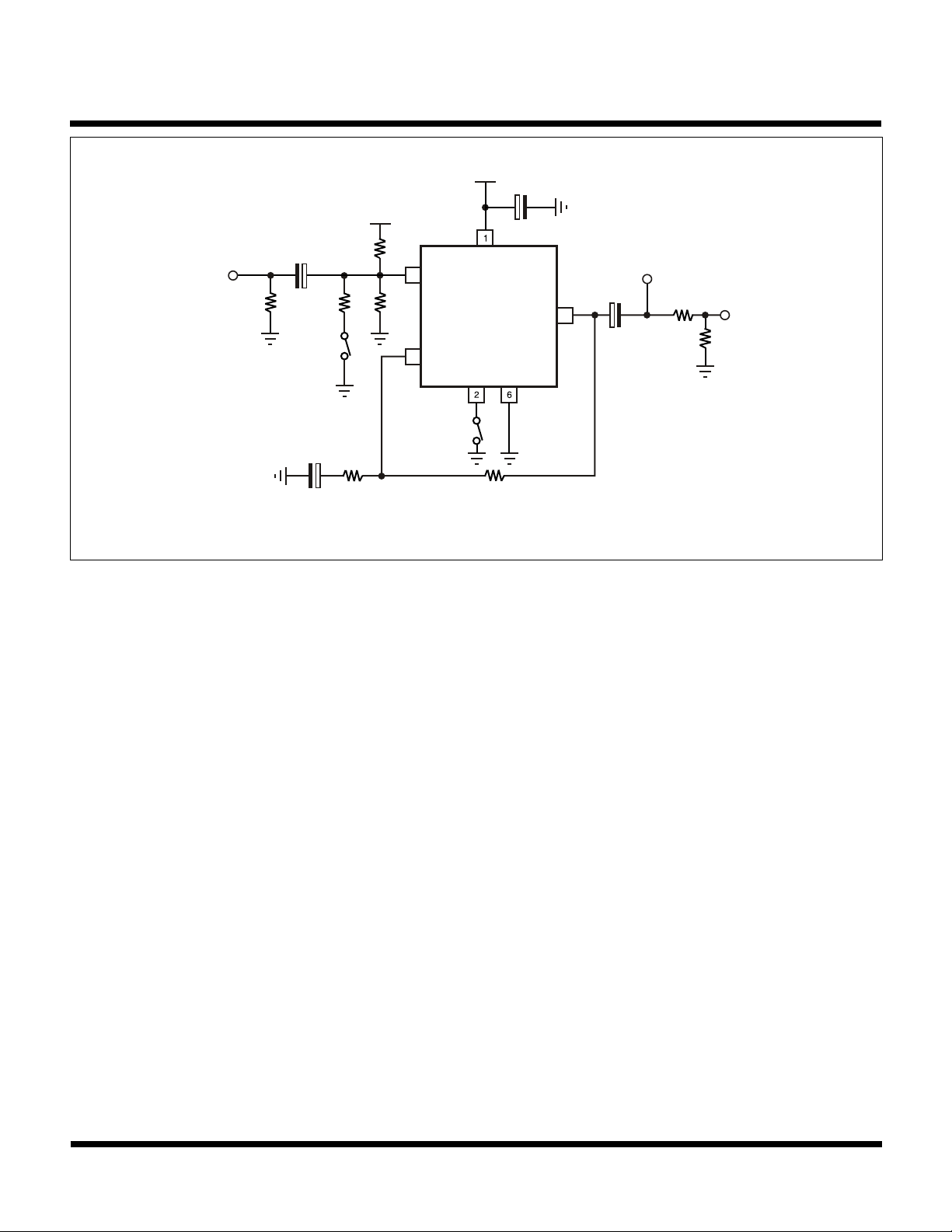
TP1
75 Ω
SW1 is turned on
only when DG and
DP are measured.
MEASUREMENT METHOD
4.7 µF
47 µF
+Input 1,2,3
+
20 kΩ
SW1
-Input 1,2,3
+
TEST CIRCUIT
V
CC
V
2 kΩ
VCC = 5.0 V
CC
10 kΩ
10 kΩ
Standby GND
2 kΩ
Common Measurement Circuit for Each Channel
+
33 µF
+
47 µF
TP2
Output 1,2,3
V
= 2.0 V
OUT
75 Ω
75 Ω
P-P
TP3
1. Supply Current (ICC)
The Pin 1 current is measured with no input signal and the Standby Pin (Pin 2) open.
2. Standby Supply Current (I
STBY
)
The Pin 1 current is measured when the Standby Pin (Pin 2) is connected to ground.
3. Standby Terminal Current (IOS)
The Pin 2 current is measured when Pin 2 is connected to ground.
4. Threshold Voltage (High to Low) (V
THL
)
The Pin 2 voltage is measured at the point which changes the device from operating mode into standby mode.
5. Threshold Voltage (Low to High) (V
TLH
)
The Pin 2 voltage is measured at the point which changes the device from standby mode into operating mode.
6. Voltage Gain (GVA)
The voltage gain equation is as follows:
GVA = 20 log10 V2/V1
Where V1 is the input voltage at TP1 and V2 is the measured output voltage at TP2.
V1 and V2 are measured for the other channels in the same manner.
7. Frequency Response (fr)
The frequency response equation is as follows:
fr = 20 log10 V2/V1
Where V1 is the measured TP2 voltage when the TP1 input frequency is set to 1 MHz and V2 is the measured TP2 voltage
when the TP1 input frequency is set to 5 MHz. Furthermore, V1 is the measured TP2 voltage when the TP1 input frequency
is set to 1 MHz and V2 is the measured TP2 voltage when the TP1 input frequency is set to 10 MHz.
V1 and V2 are measured for the other channels in the same manner.
January 2000 TOKO, Inc. Page 3
 Loading...