TOKO TK15322MTL Datasheet

TK15322
u
u
Audio Analog Switch
FEATURES
■ Wide Operating Voltage Range (2 to 14 V)
■ Low Distortion (typ. 0.004%)
■ Wide Dynamic Range (typ. 6 V
P-P
)
■ Low Output Impedance (typ. 20 Ω)
■ Low Switching Noise (typ. 3 mV)
DESCRIPTION
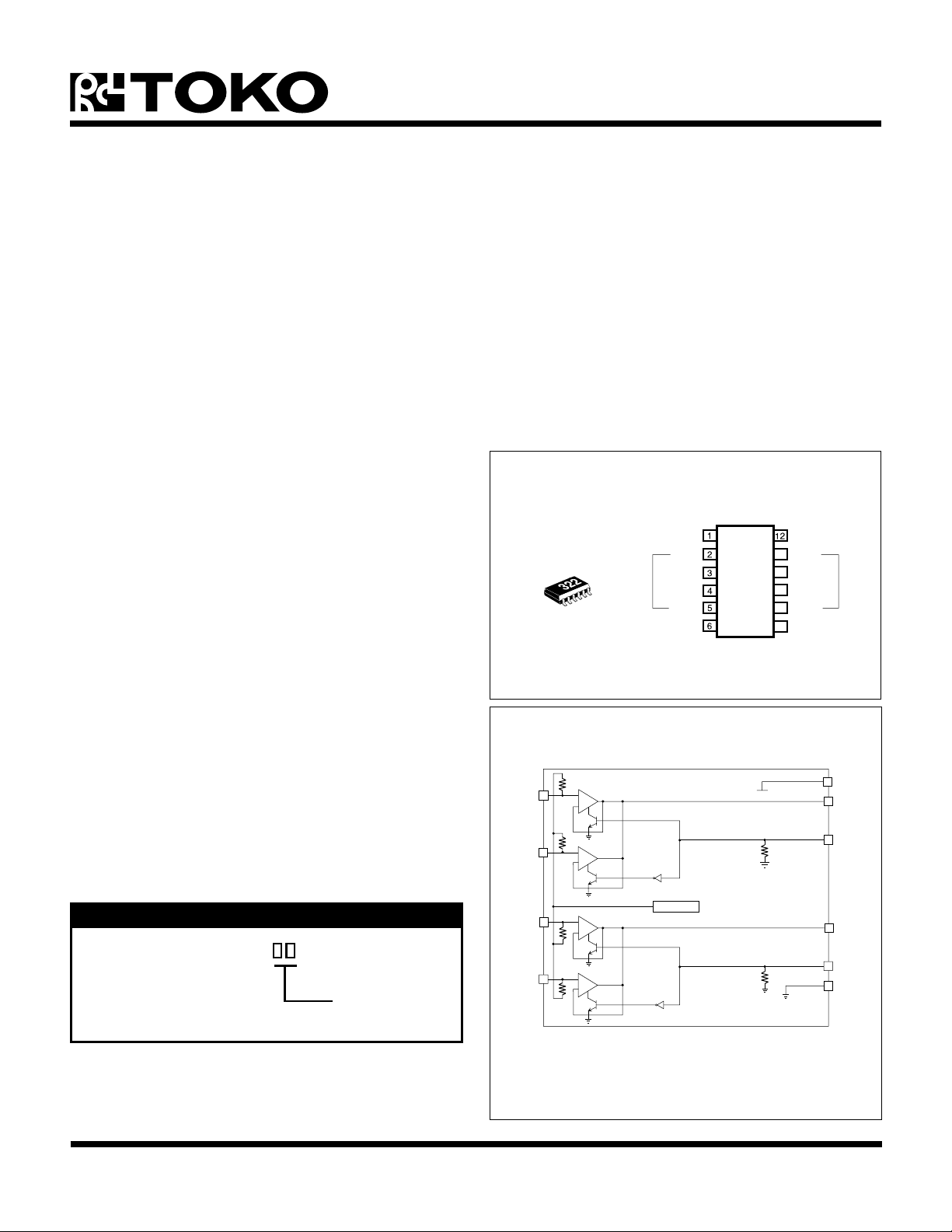
The TK15322M is an Analog Switch IC that was developed
for audio frequency. Function is to select one output from
two inputs in a device that includes two circuits, and the
channel can be changed by high level. The TK15322M
has a mono-power supply and the input bias is a built-in
type (VCC / 2 V). Because the distortion is very low, the
TK15322M fits various signals switching. It is best suited
for Hi-Fi devices. Operating voltage is wide, the circuit
plan is simple. The TK15322M is available in a small
plastic surface mount package (SSOP-12).
APPLICATIONS
■ Audio Systems
■ Radio Cassettes
1ch-in 2ch-in
TK15322
V
CC
Bch
OUT
Ach
1KEY
NC
GND
11
Bch
10
OUT
9
Ach
8
2 KEY
NC
7
BLOCK DIAGRAM
V
CC
1 ch o
1KEY
2 ch o
2KEY
GND
ORDERING INFORMATION
TK15322M
1ch-in
2ch-in
Ach
Bch
Ach
Bch
+
-
+
-
+
-
+
-
Reg. (VCC / 2)
Tape/Reel Code
TAPE/REEL CODE
TL: Tape Left
June 1999 TOKO, Inc. Page 1

TK15322
ABSOLUTE MAXIMUM RATINGS
Supply Voltage ......................................................... 15 V
Power Dissipation (Note 4) ................................ 350 mW
Storage Temperature Range ................... -55 to +150 °C
ANALOG SWITCH SECTION
Signal Input Voltage ........................ -0.3 V to VCC + 0.3 V
Signal Output Current ............................................. 3 mA
Operating Temperature Range ...................-20 to +75 °C
CONTROL SECTION
Input Voltage ................................... -0.3 V to VCC + 0.3 V
Operating Voltage Range................................. 2 to 14 V
Maximum Input Frequency..................................100 kHz
TK15321M ELECTRICAL CHARACTERISTICS
Test conditions: V
LOBMYSRETEMARAPSNOITIDNOCTSETNIMPYTXAMSTINU
I
CC
V
LI
V
HI
Z
NI
DHTnoitrotsiDcinomraHlatoTV
N
L
OSInoitalosI
= 8.0 V, T
CC
= 25 °C, unless otherwise specified.
A
tnerruCylppuS 2.45.6Am
NOITCESLORTNOCYEK
leveLwoLegatloVtupnI1etoN3.0-8.0+V
leveLhgiHegatloVtupnI8.1V
ecnadepmItupnI 05kΩ
NOITCESHCTIWSGOLANA
NI
esioNlaudiseR2etoN01smrVµ
V
NI
3etoN
3.0+V
CC
zHk1=f,smrV1=400.0800.0%
,zHk01=f,smrV1=
57-Bd
PESnoitarapeS
V
NI
3etoN
,zHk01=f,smrV1=
NYDleveLlangiStupnImumixaM%1.0=DHT,zHk1=f0.2smrV
AVGniaGegatloVzHk02~=f0Bd
V
tnec
∆V
tnec
R
NI
Z
TUO
Note 1: The KEY input equivalent circuit is shown to the right.
1 channel and 2 channel is the separate action by 1Key pin and
2 key pin. When the control pin is open, it is outputted low level. Then the A channel input signal is
outputted. The change is carried out at high level.
Note 2: The specification means a value as measurement-input terminal connects to ground through a capacitor.
Note 3: ISO is a cross talk between A channel and B channel, SEP is a cross talk between 1 channel and 2
channel. The specification means a value as measurement-input termianl connects to ground through 10
kΩ resistor and capacitor.
Note 4: Power dissipation is 350 mW when mounted as recommended. Derate at 3.0 mW/°C for operation above
25°C.
egatloV
ecnereffiD
lanimreTtuptuO-tupnI
egatloVlanimreTtuptuO
ecnatsiseRsaiBtupnI 56kΩ
ecnadepmItuptuOecnadepmICD02
V
CC
tuptuo2/8.30.42.4V
lennahcemasneewteB331Vm
Input Key
08-Bd
Ω
Logic
Page 2 June 1999 TOKO, Inc.

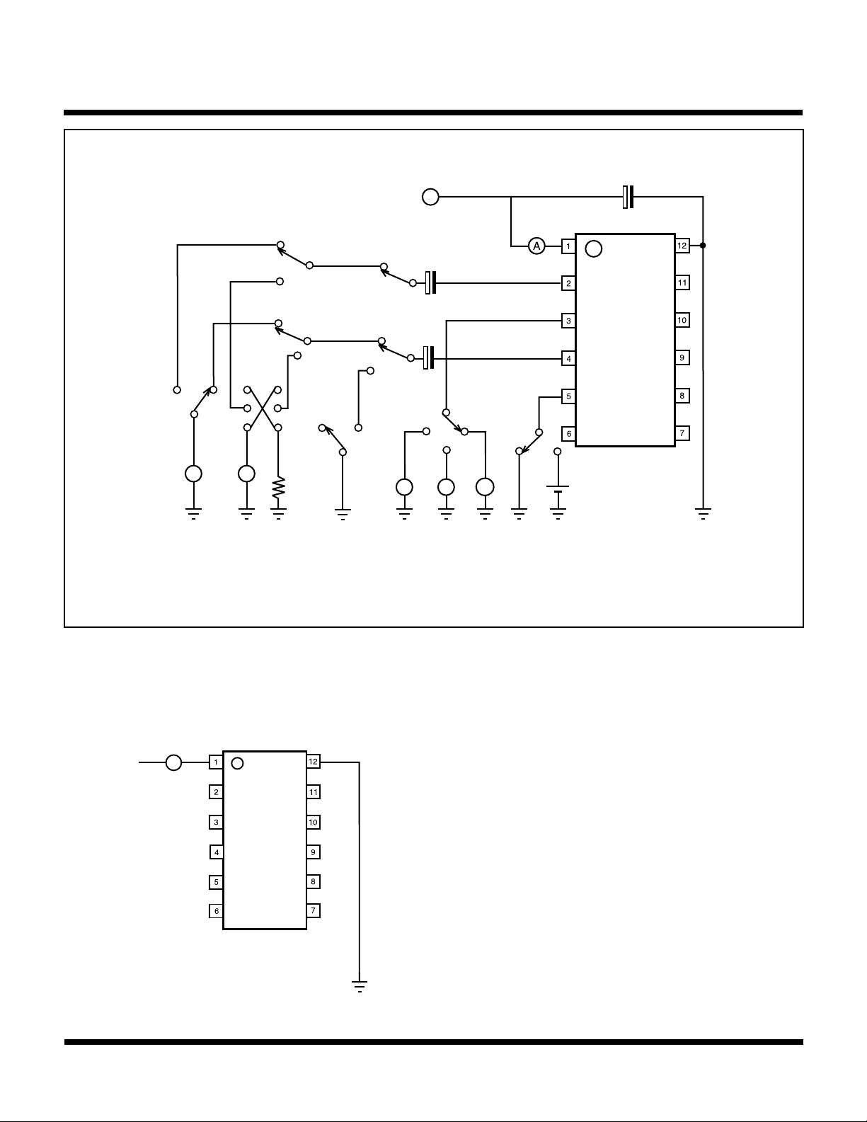
TEST CIRCUITS AND METHODS
V
CC
TK15322
33 µF
+
1 kHz
1 Vrms
or
2 Vrms
SW9
~
10 kHz
1 Vrms
SW8
~
1: The above condition represents 1ch.
2: The above conditions distortion rate of 1-Ach and dynamic range measurement.
3: SW5 is for residual noise measurement.
4: SW8 is for cross talk (ISO or SEP) measurement.
SUPPLY CURRENT (FIGURE 1)
SW6
SW7
10 kΩ
SW5
SW3
SW4
SW2
V
~
10 µF
+
10 µF
+
SW1
LH
V
THD
_
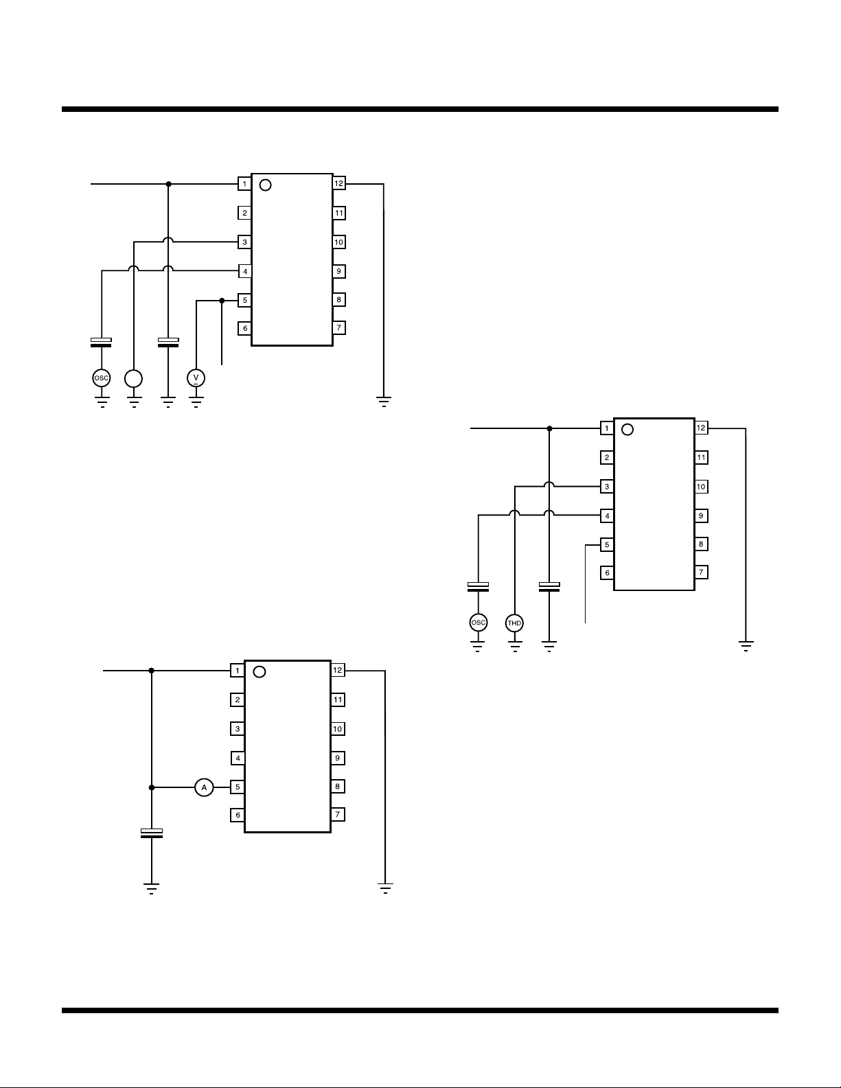
CONTROL LOW/HIGH LEVEL (FIGURE 2)
This current is a consumption current with a nonloading
condition.
1) Measure the inflow current to Pin 1 from VCC. This
current is the supply current.
CC
AV
This level is to measure the threshold level.
1) Input, the VCC to Pin 1. (This condition is the same with
other measurements, omitted from the next for simplicity)
2) Input to Pin 4 with sine wave (f = 1 kHz, VIN = 1 Vrms).
3) Connect an oscilloscope to Pin 3.
4) Drop the control voltage from VCC gradually, until the
sine wave appears at the oscilloscope. This voltage is
the threshold level when the wave appears.
Figure 1
June 1999 TOKO, Inc. Page 3

TK15322
V
CC
Cont.
++
TEST CIRCUITS AND METHODS (CONT.)
V
CC
++
~
Cont.
Figure 2
CONTROL INPUT IMPEDANCE (FIGURE 3)
This is the input resistance of control terminal.
1) Measure the inflow current from VCC to Pin 5.
2) Calculate: IMP = VCC / Inflow Current
This resistance is the input impedance.
TOTAL HARMONIC DISTORTION (FIGURE 4)
Use the lower distortion oscillator for this measurement
because distortion of the TK15322 is very low.
1) Pin 5 is in the open condition, or low level.
2) Connect a distortion analyzer to Pin 3.
3) Input the sine wave (1 kHz, 1 Vrms) to Pin 4.
4) Measure the distortion of Pin 3. This value is the
distortion of 1-Ach.
5) Next connect Pin 5 to the VCC, or high level.
6) Input the same sine wave to Pin 2.
7) Measure in the same way. This value is the distortion
of 1-Bch.
V
CC
Figure 4
VOLTAGE GAIN (FIGURE 5)
This is the output level against input level.
1) Pin 5 is in the open condition, or low level.
2) Connect AC volt meters to Pin 4 and Pin 3.
(Using the same type meter is best)
3) Input a sine wave (f = max. 20 kHz, 1 Vrms) to Pin 4.
+
4) Measure the level of Pin 4 and name this V1.
5) Measure the level of Pin 3 and name this V2.
6) Calculate Gain = 20 Log (( |V2 - V1| )/V1)
V1<V2 + Gain, V1>V2 - Gain
This value is the voltage gain of 1-Ach.
Figure 3
7) Next, connect Pin 5 to the VCC, or high level.
8) Input the same sine wave to Pin 2.
9) Measure and calculate in the same way.
This value is the voltage gain of 1-Bch.
Page 4 June 1999 TOKO, Inc.
 Loading...