TOKO TK15220MTL Datasheet

TK15220
Audio Analog Switch
FEATURES
■ Wide Operating Voltage Range (2 to 13 V)
■ Low Distortion (typ. 0.004%)
■ Wide Dynamic Range (typ. 6 V
P-P
)
■ Low Output Impedance (typ. 20 Ω)
■ Protection at Output Terminal.
DESCRIPTION
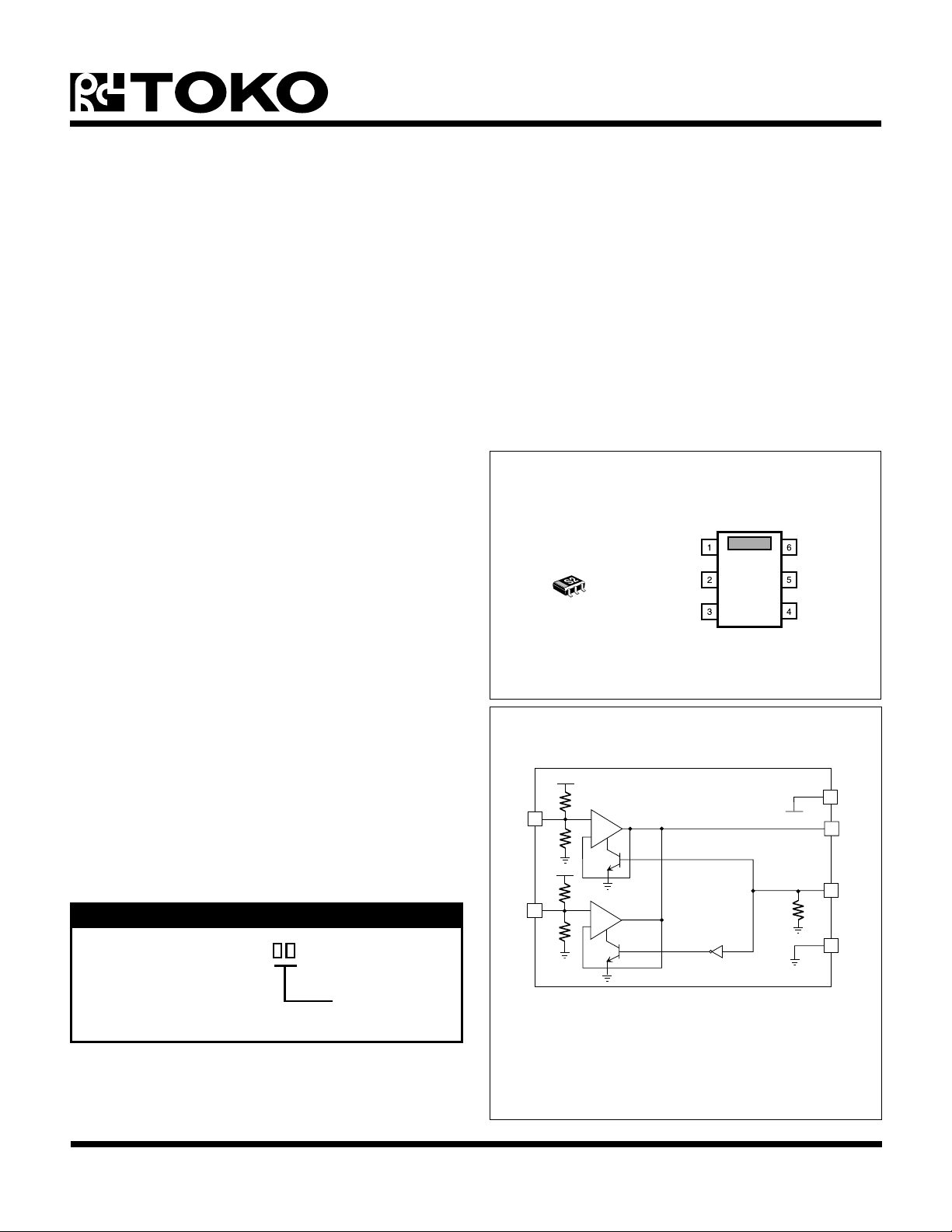
The TK15220M is an Analog Switch IC that was developed
for audio frequency applications. The function of the IC is
to select one output from two input channels. The channel
selection can be controlled by a higher level by the addition
of an external resistor. The TK15220M operates from a
single power supply with the input bias built-in (VCC/2).
Because the distortion is very low, the TK15220M is
suitable for various signal switching applications, especially
Hi-Fi devices. The TK15220M offers a wide operating
voltage range with simple associated circuitry.
APPLICATIONS
■ Audio Systems
■ Radio Cassettes
20P
TK15220
IN A
OUT
IN B
V
CC
GND
KEY
The TK15220M is available in the small SOT23L-6 plastic
surface mount package.
ORDERING INFORMATION
TK15220M
Tape/Reel Code
TAPE/REEL CODE
TL: Tape Left
IN A
IN B
V
CC
V
CC
BLOCK DIAGRAM
+
-
+
-
V
CC
V
CC
OUT
KEY
GND
June 1999 TOKO, Inc. Page 1

TK15220
ABSOLUTE MAXIMUM RATINGS
Supply Voltage ......................................................... 14 V
Operating Voltage Range................................. 2 to 13 V
Power Dissipation (Note 4) ................................ 200 mW
Storage Temperature Range ................... -55 to +150 °C
Operating Temperature Range ...................-20 to +75 °C
CONTROL SECTION
Input Voltage .................................... -0.3 V to VCC +0.3 V
TK15210M ELECTRICAL CHARACTERISTICS
Test conditions: V
LOBMYSRETEMARAPSNOITIDNOCTSETNIMPYTXAMSTINU
= 8.0 V, T
CC
= 25 °C, unless otherwise specified.
A
ANALOG SWITCH SECTION
Signal Input Voltage ......................... -0.3 V to VCC +0.3 V
Signal Output Current ............................................. 3 mA
Maximum Input Frequency..................................100 kHz
Lead Soldering Temperature (10 s) ...................... 235 °C
I
CC
tnerruCylppuS 5.20.5Am
NOITCESLORTNOCYEK
V
LI
V
HI
I
R
ecnatsiseRtupnI 03kΩ
leveLwoLegatloVtupnI1etoN3.0-6.0+V
leveLhgiHegatloVtupnI0.2V
CC
NOITCESHCTIWSGOLANA
DHTnoitrotsiDcinomraHlatoTV
N
L
esioNlaudiseR2etoN01smrVµ
TCklaTssorC
NI
V
NI
3etoN
zHk1=f,smrV1=400.0800.0%
,zHk01=f,smrV1=
08-57-Bd
NYDleveLlangiStupnImumixaM%1.0=DHT,zHk1=f0.2smrV
AVGniaGegatloVzHk02~=f0Bd
V
tnec
∆V
tnec
Z
NI
Z
TUO
Note 1: The KEY input equivalent circuit is shown to the right. When the control pin
is open, the input is pulled down to a low level. This applies the channel A
input signal to the output. A high level changes the output to the channel B
input signal.
egatloV
ecnereffiD
lanimreTtuptuO-tupnI
egatloVlanimreTtuptuO
ecnadepmItupnIecnadepmICD63kΩ
ecnadepmItuptuOecnadepmICD02
V
CC
tuptuo2/8.30.42.4V
lennahcemasneewteB81Vm
Key Input
Logic
3.0+V
Ω
Note 2: This value measured with a capacitor connected between the input terminal and ground. See Figure 7.
Note 3: This value measured with a 5 kΩ resistor and series capacitor connected between the input terminal and ground. See Figure 8.
Note 4: Power dissipation is 200 mW when mounted as recommended. Derate at 1.6 mW/°C for operation above 25°C.
Page 2 June 1999 TOKO, Inc.

TEST CIRCUITS AND METHODS
TK15220
V
CC
SW6
SW3
SW7
SW4
SW9
1 kHz
1 Vrms
2 Vrms
SW8
10 kHz
1 Vrms
~
or
~
5 kΩ
SW5
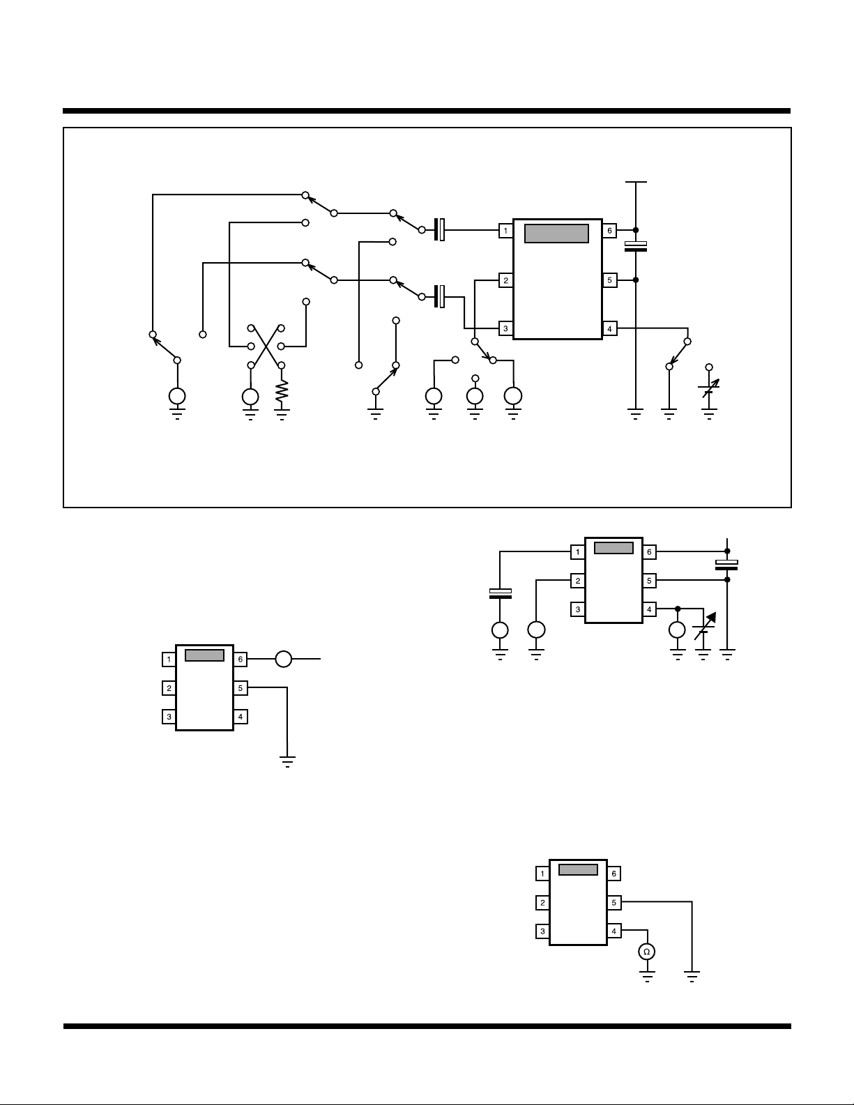
1: The above condition tests the dynamic range measurement for channel A.
2: SW5 is for residual noise measurement.
3: SW8 is for cross talk measurement.
SUPPLY CURRENT (FIGURE 1)
This current is a consumption current with a nonloading
condition.
1) Measure the inflow current to Pin 6 from VCC. This
current is the supply current.
V
CC
A
10 µF
10 µF
V
~
+
+
SW2
V
THD
_
+
OSC
~
+
SW1
V
CC
+
V
Figure 2
KEY INPUT IMPEDANCE (FIGURE 3)
This impedance means the base resistance of the input
transistor (see terminal circuit on page 8).
Figure 1
1) Remove VCC of Pin 6.
2) Measure the resistance value by measuring instrument.
CONTROL LOW/HIGH LEVEL (FIGURE 2)
(e.g., multimeter etc.)
This level is to measure the threshold level.
1) Input the VCC to Pin 6. (This condition is the same with
the other measurements, omitted from the next for
simplicity.)
2) Input to Pin 1 with a sine wave (1 kHz, 1 Vrms).
3) Connect an oscilloscope to Pin 2.
4) Elevate the Pin 4 voltage from 0 V gradually, until the
sine wave appears at the oscilloscope. This voltage is
the threshold level when the wave appears.
Figure 3
June 1999 TOKO, Inc. Page 3

TK15220
V
CC
+
+
~
V
~V~
V1 V2
V
CC
+
+
~
V
~
THD
TEST CIRCUITS AND METHODS (CONT.)
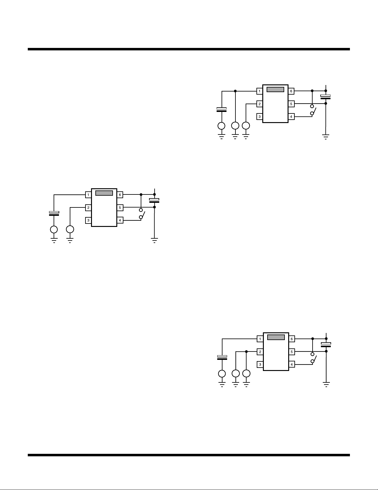
TOTAL HARMONIC DISTORTION (FIGURE 4)
Use the lower distortion oscillator for this measurement
because the distortion of the TK15220 is very low.
1) Pin 4 is in the open condition, or high level.
2) Connect a distortion analyzer to Pin 2.
3) Input the sine wave (1 kHz, 1 Vrms) to Pin 1.
4) Measure the distortion of Pin 2. This value is the
distortion of Ach.
5) Next connect Pin 4 to the VCC, or high level.
6) Input the same sine wave to Pin 3.
7) Measure in the same way. This value is the distortion
of Bch.
V
CC
+
Figure 5
MAXIMUM INPUT LEVEL (FIGURE 6)
+
THD
~
Figure 4
VOLTAGE GAIN (FIGURE 5)
This is the output level against the input level.
1) Pin 4 is in the open condition, or low level.
2) Connect AC volt meters to Pin 1 and Pin 3.
(Using the same type meter is best)
3) Input a sine wave (1 kHz) to Pin 1 (f = optional up to max.
20 kHz, 1 Vrms).
4) Measure the level of Pin 1 and name this V1.
5) Measure the level of Pin 2 and name this V2.
6) Calculate Gain = 20 Log (( |V2 - V1| )/V1)
V1<V2 = + Gain, V1>V2 = - Gain
This value is the voltage gain of Ach.
7) Next, connect Pin 4 to the GND, or high level.
8) Input the same sine wave to Pin 3.
9) Measure and calculate in the same way.
This value is the voltage gain of Bch.
This measurement measures at the output side.
1) Pin 4 is in the open condition, or low level.
2) Connect a distortion analyzer and an AC volt meter to
Pin 2.
3) Input a sine wave (1 kHz) to Pin 1 and elevate the voltage
from 0 V gradually until the distortion gets to 0.1% at Pin
2.
4) When the distortion amounts to 0.1%, stop elevating and
measure the AC level of Pin 2.
This value is the maximum input level of Ach.
5) Next, connect Pin 4 to the VCC, or high level.
6) Input the same sine wave to Pin 2.
7) Measure in the same way.
This value is the maximum input level of Bch.
Figure 6
Page 4 June 1999 TOKO, Inc.
 Loading...