TOKO TK15125MTL Datasheet

TK15125
Dual Supply Grand Earthing System Audio Signal Mute IC
FEATURES
■ Wide Voltage Range (±2.5 to ±5.5 V)
■ High Volume Attenuation (typ. -89dB)
■ Very Low Signal Distortion (typ. 0.0025%)
■ High Maximum Input Voltage (max. 5.2 V
P-P
)
■ Very Low Standby Current (typ. 0.6 mA)
■ Minimal External Component Circuitry
DESCRIPTION
The TK15125M is a dual power supply Mute IC of the
Grand Earthing System that was developed as a low
frequency signal attenuator for audio products.
The mute function includes two channels which operate
simultaneously by one control key.
The optional time for the Attack/Release action can be set
up by an external timing control capacitor.
APPLICATIONS
■ Audio Systems
■ Television
■ VTR
■ MD
■ CD
TK15125
OUT/IN 1
IN/OUT 1
GND 1
GND 2
GND 3
IN/OUT 2
OUT/IN 2
V
DD
MUTE-C
NC
NC
NC
CONTROL
V
SS
The TK15125M is available in a SOP-14 Surface Mount
Package.
ORDERING INFORMATION
TK15125M
Tape/Reel Code
TAPE/REEL CODE
TL: Tape Left
DD
MUTE-C
V
CONTROL DRIVER TIMING
OUT/IN 1
IN/OUT 1
BLOCK DIAGRAM
NC
GND 2
NC
GND 3
NC
GND 1
CONTROL
IN/OUT 2
SS
V
OUT/IN 2
Control
Lo: Mute off
Hi: Mute on
July 1999 TOKO, Inc. Page 1

TK15125
ABSOLUTE MAXIMUM RATINGS
Supply Voltage ......................................................... ±6 V
Power Dissipation (Note 3) ................................ 350 mW
Input Frequency ..................................................100 kHz
Storage Temperature Range ................... -55 to +150 °C
Operating Temperature Range ...................-20 to +60 °C
Signal Input Voltage ......................................... VSS to V
TK15121M ELECTRICAL CHARACTERISTICS
Test conditions: V
LOBMYSRETEMARAPSNOITIDNOCTSETNIMPYTXAMSTINU
V
DD
V
SS
I
)FFO(DD
I
)NO(DD
TTAnoitaunettAR
IC
NO
IC
FFO
VWS
FFO
= ±5 V, T
CC
egatloV
= 25 °C, f = 1 kHz, V
A
egatloVgnitarepO
ffOetuM,tnerruCgnitarepO 6.09.0Am
nOetuM,tnerruCgnitarepO 0.210.71Am
NI
tnerruCegrahCnOetuM0.80.210.81Aµ
tnerruCegrahcsiDffOetuM)2etoN(8.10.30.5Aµ
ffOetuM,WSlortnoCetuM
SIN
= 5 V
unless otherwise specified.
P-P
003= Ω )1etoN(58-98-Bd
DD
5.20.55.5V
5.2-0.5-5.5-V
V
SS
V
4.0+V
SS
VWS
NO
IWS
NO
V
TASO
egatloV
tnerruC
1DHT
2DHTNOretliFA-SIJ7000.00300.0%
noitrotsiD
nOetuM,WSlortnoCetuM
V
nOetuM,WSlortnoCetuM
egatloVCDtuptuOnOetuM 4.27.3Vm
cinomraHlatoTffOetuM
4.2+V
SS
DD
6152Aµ
5200.00700.0%
V
AVGniaGegatloVzHk02~=Bd5.0-05.0+Bd
V
)XAM(NI
RMecnatsiseRnoitaunettArennI861042213
Note 1: If an RIN other than 300 Ω is used, the volume attenuation and attack/release times change.
Note 2: In the standard application a capacitor is connected between Pin 13 and VSS. Attack is the term used to describe the action of changing the
unit from ‘mute off’ to ’mute on’. Release is the term used to describe the action of changing the unit from ‘mute on’ to ‘mute off’. The standard
timing control capacitance is 0.047 µF.
Note 3: Power dissipation is 350 mW when mounted as recommended. Derate at 2.8 mW/°C for operation above 25°C.
egatloVtupnImumixaM%10.0<DHT2.5V
P-P
Ω
Page 2 July 1999 TOKO, Inc.

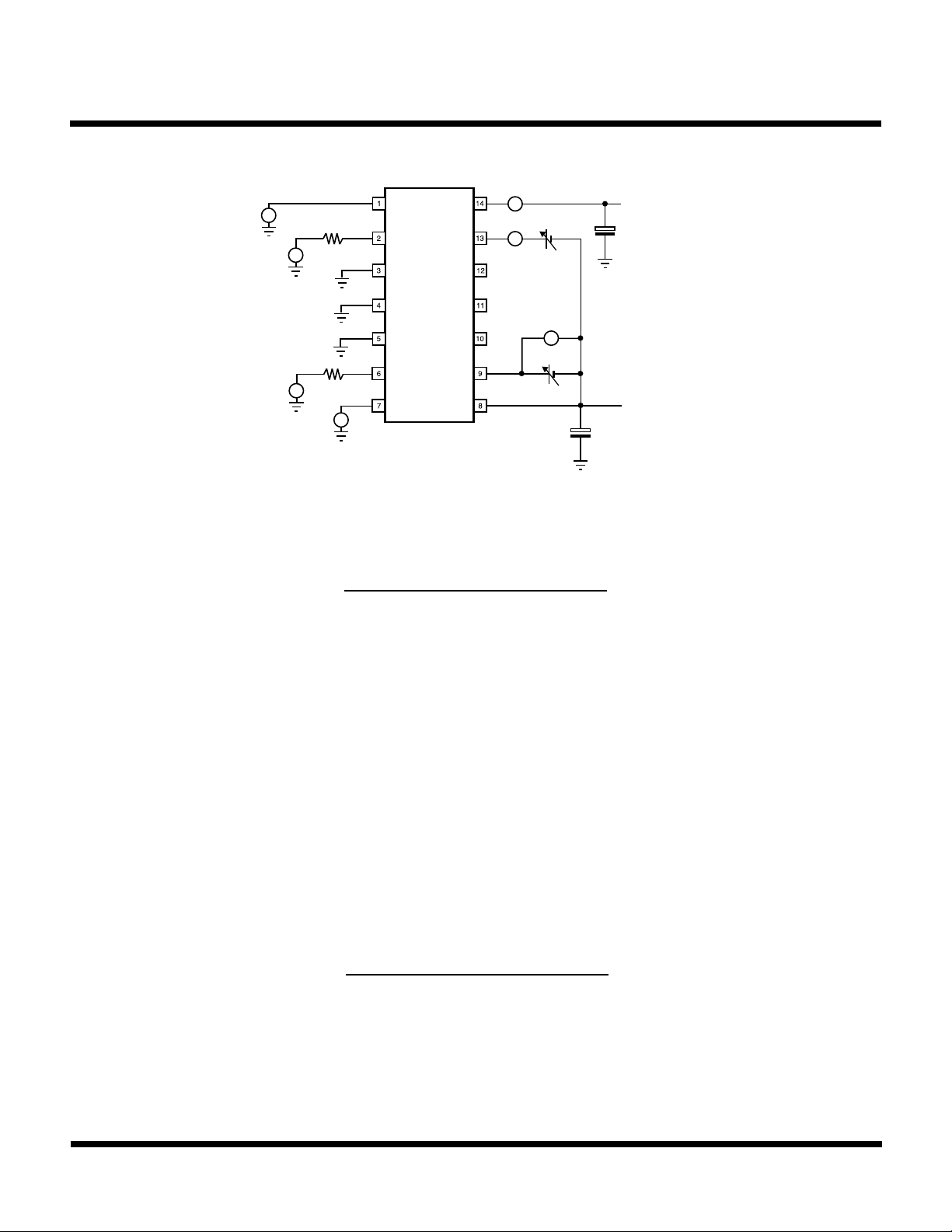
TEST CIRCUIT AND TESTING METHODS
V
+
+5 V
22 µF
DD
VM
300 Ω
SG
A1
A2
NC
TK15125
NC
NC
V1
V
SS
-5 V
22 µF
+
SG
TESTING METHODS
1) POWER SUPPLY CURRENT
GND
300 Ω
VM
· ‘MUTE OFF’ Mode
Measure current ‘A1’ while control, Pin 9, is ‘Lo’ (or open).
· ‘MUTE ON’ Mode
Measure current ‘A1’ while control, Pin 9, is ‘Hi’.
2) ATTENUATION VOLUME
· Attenuation is calculated by the following equation while control, Pin 9, is ‘Hi’:
Pin 1(Pin 7) output AC voltage
ATT = 20Log
(
Pin 2(Pin 6) input AC voltage
)
3) CAPACITOR PIN CHARGING AND DISCHARGING CURRENT
· Charging Current
Measure outflow current ‘A2’ while control, Pin 9, is ‘Hi’ and the voltage at Pin 13 is VSS + 0.75 V.
· Discharging Current
Measure inflow current ‘A2’ while control, Pin 9, is ‘Lo (or open)’ and the voltage at Pin 13 is VSS + 0.75 V.
4) CONTROL SWITCH VOLTAGE
· ‘MUTE OFF’ Mode
Gradually elevate Pin 9 voltage above VSS. When the Attack action (Mute On) is implemented at Pin 1 (Pin 7),
measure the voltage ‘V1’.
· ‘MUTE ON’ Mode
Gradually lower Pin 9 voltage below VDD. When the Release action (Mute Off) is implemented at Pin 1 (Pin 7),
measure the voltage ‘V1’.
5) ‘MUTE ON’ OUTPUT DC VOLTAGE
· Measure output voltage at Pin 1 (Pin 7) while control, Pin 9, is ‘Hi’ and there is no input.
6) TOTAL HARMONIC DISTORTION
· Measure the distortion of the Pin 1 (Pin 7) output while control, Pin 9, is ‘Lo’ (or open).
7) SIGNAL VOLTAGE GAIN
· Signal gain is calculated by the following equation while control, Pin 9, is ‘Lo’ (or open).
Pin 1(Pin 7) output AC voltage
GV = 20Log
(
Pin 2(Pin 6) input AC voltage
)
8) INNER ATTENUATION RESISTANCE
· Using a multimeter, measure the resistance between Pin 1 (Pin 7) and Pin 2 (Pin 6) while the power supply is
off.
9) MAXIMUM INPUT SIGNAL VOLTAGE
· While control, Pin 9, is ‘Lo’ (or open), gradually elevate Pin 2 (Pin 6) voltage above 0 V
becomes 0.01% at the output of Pin 1 (Pin 7), measure the AC voltage.
. When the distortion
P-P
July 1999 TOKO, Inc. Page 3
 Loading...