TOKO TK11850LTL Datasheet

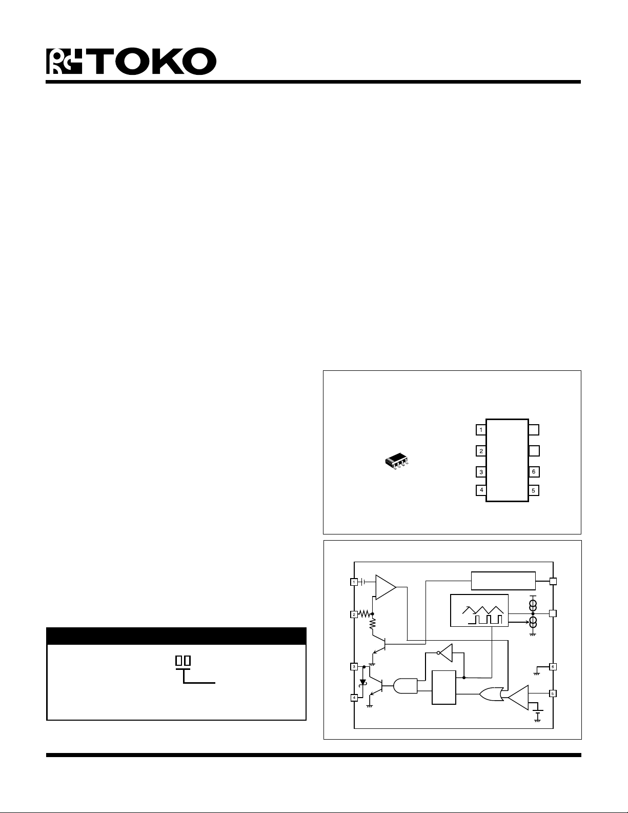
TK11850L
I
S
EXT
V
IN
V
OUT
GND
7
C
X
8
EN
V
FB
+
-
+
-
BAND GAP REFERENCE
OSC
C
X
CLK
0.86 V
0.3 V
CLK
S
R
Q
V
REF
0.525 V
ERROR
COMP
IS COMP
0.1 V
WHITE LED DRIVER
FEATURES
n Very High Speed Adjustable OSC (Max 800 kHz)
n Very Wide Operating Voltage Range (2.3 V to 10 V)
n Low Loss Detector (Low Reference Voltage:
V
= 0.5 V)
REF
n Operates with Toko D31FU Miniature Coil (Current
Limited by Input Current Sensor)
n Internal Switching Transistor
n Internal Diode
n Active High On / Off Control
n Available Intensity Control Using EN Pin with PWM
Signal
n Very Small SOT23L-8 Surface Mount Package
DESCRIPTION
The TK11850L is a pulse skipping step-up DC-DC converter
IC designed for White LED driver applications with the
following built in: a very high current switching transistor
(400 mA peak), an inductor current limit detector, low
voltage reference (Vref = 0.5 V), high speed oscillator, an
error comparator, a rectifier diode (for small power output)
and an ON/OFF control. The IC works with a very wide
operating supply range (2.3 V to 10 V) and the adjustable
output voltage can be set as high as 20 V. The device is in
the ON state when the EN pin is pulled to a high level. Using
the very small TK11850L and a few external components,
battery powered systems with LCD displays such as digital
cameras and cellular phones can be effectively backlit with
white LEDs. The white LEDs are connected in series and
driven at a constant current resulting in uniform brightness
and high efficiency. This IC has an oscillator, which allows
the designer to set the operating frequency by an external
capacitor with the output controlled by pulse skipping. The
reference voltage is a very low 0.5 V, achieving high
efficiency operation with the constant current output. A
small coil can be used because the inductor current limit
detector circuit limits the peak current (caused by an input
APPLICATIONS
n LED Backlighting and Frontlighting
n LED Flashlights
n Step-up DC-DC Converters
voltage increase or the inrush current as start-up) that flows
through the coil. The ON /OFF control is built-in and the
circuit current can be decreased when the EN pin is low
(standby mode). The white LEDs can be dimmed by
applying a PWM signal to the EN (ON/OFF control) pin. With
this method, the white LED brightness is still controlled by
constant current resulting in constant chromaticity.
The TK11850L is available in the SOT23L-8 surface mount
package.
TK11850
V
IN
I
S
EXT
V
OUT
BLOCK DIAGRAM
8EN
C
7
X
GND
V
FB
ORDERING INFORMATION
May 2001 TOKO, Inc. Page 1
TK11850L
Tape/Reel Code
TAPE/REEL CODE
TL: Tape Left

TK11850L
ABSOLUTE MAXIMUM RATINGS
Supply Voltage........................................................ 20 V
Switching Voltage .................................................... 20 V
Operating Voltage Range ............................... 2.3 to 10 V
Power Dissipation (Note 1) ................................. 400 mW
Storage Temperature Range .....................-55 to +150 °C
TK11850 ELECTRICAL CHARACTERISTICS
Test Conditions: VIN = 3 V, V
LOBMYSRETEMARAPSNOITIDNOCTSETNIMPYTXAMSTINU
=VEN = VIN, V
IS
)NIP
C(NOITCESROTALLICSO
X
= Open, VFB = GND, CX = 100 pF, TA = 25 °C, unless otherwise specified.
EXT
Operating Temperature Range.....................-30 to +85 °C
Switching Peak Current....................................... 400 mA
Diode Current ........................................................ 10 mA
Maximum Frequency ...................................... ~ 800 kHz
I
GHC
I
SID
I/
I
SID
V
V
V
CSO
V
TIMIL
I
nIsI
C
X
C
X
GHC
C
)HGIH(XC
X
C
)WOL(XC
X
C
X
oitaRtnerruC
egatloV
I
S
tnerruCgnigrahCV
tnerruCgnigrahcsiDV
XC
XC
egrahcsiDdnaegrahC
+egatloVdlohserhTV
-egatloVdlohserhTV
XC
XC
V1.0=612203
V0.1=539456
2.2
Ita
0= mA018068019Vm
GHC
Ita
0= mA062003043Vm
SID
egatloVnoitallicsO)-htV(-)+htV(025065006Vm
)NIP
I(NOITCESROTARAPMOCGNITIMILTNERRUC
S
esneStimiLtnerruC
V
tnerruCsaiBniPV
V=
TIMIL
V=
NI
V-
NI
SI
V3=50151
SI
277728Vm
mA
mA
mA
)NIPTXE(NOITCESHCTIWSTUPTUO
V
taS,WS
I
ffO,WS
rotsisnarTtuptuO
egatloVnoitarutaS
ffOrotsisnarTtuptuO
tnerruCegakaeL
V
XC
V
BF
I,V0=
WS
V,V1=
TXE
Am002=2.04.0V
V02=10.02
mA
V(NOITCESROTARAPMOCKCABDEEF
V
FER
I
nIBF
Note 1: Power dissipation is 400 mW when mounted. Derate at 3.2 mW / °C for operation above 25 °C.
V
BF
egatloVecnerefeR505.0525.0545.0V
tnerruCtuptuOniPV
)NIP
BF
BF
V4.0=2-3.0-
Page 2 May 2001 TOKO, Inc.
mA

TK11850 ELECTRICAL CHARACTERISTICS (CONT)
Test Conditions: VIN = 3 V, VIS =VEN = VIN, V
LOBMYSRETEMARAPSNOITIDNOCTSETNIMPYTXAMSTINU
)NIPNE(NOITCESNWODTUHS
= Open, VFB = GND, CX = 100 pF, TA = 25 °C, unless otherwise specified.
EXT
TK11850L
V
V
I
V
V
V
V
I
I
)HGIH(NE
)WOL(NE
nINE
F
NI
)WOL(NI
)HGIH(NI
)ffO(CC
)nO(CC
V(NOITCES
NI
egatloVdrawroFI
)NIP
+egatloVdlohserhTNEedoMnO2V
-egatloVdlohserhTNEedoMnwodtuhS6.0V
tnerruCsaiBniPNEV
V-NIPTXE(NOITCESEDOID
)NIP
TUO
V=
NI
D
V3=258
NE
Am01=57.0V
mA
potSegatloVwoL7.10.23.2V
potStuptuOegatloVhgiH115.2141V
tnerruCylppuSnwodtuhSV
tnerruCylppuStnecseiuQV
v0=10.01
NE
V1=15.12Am
BF
mA
eulaVecnerefeR
I
η
ycneiciffE
DAOL
V
NI
V,Am02=
TUO
)2etoN(V6.3=
,V5.61=
87%
Note 2: This value is different depending on the components used, circuit conditions, etc. Thus, this is reference data only. Refer to Reference
data test circuit.
May 2001 TOKO, Inc. Page 3

TK11850L
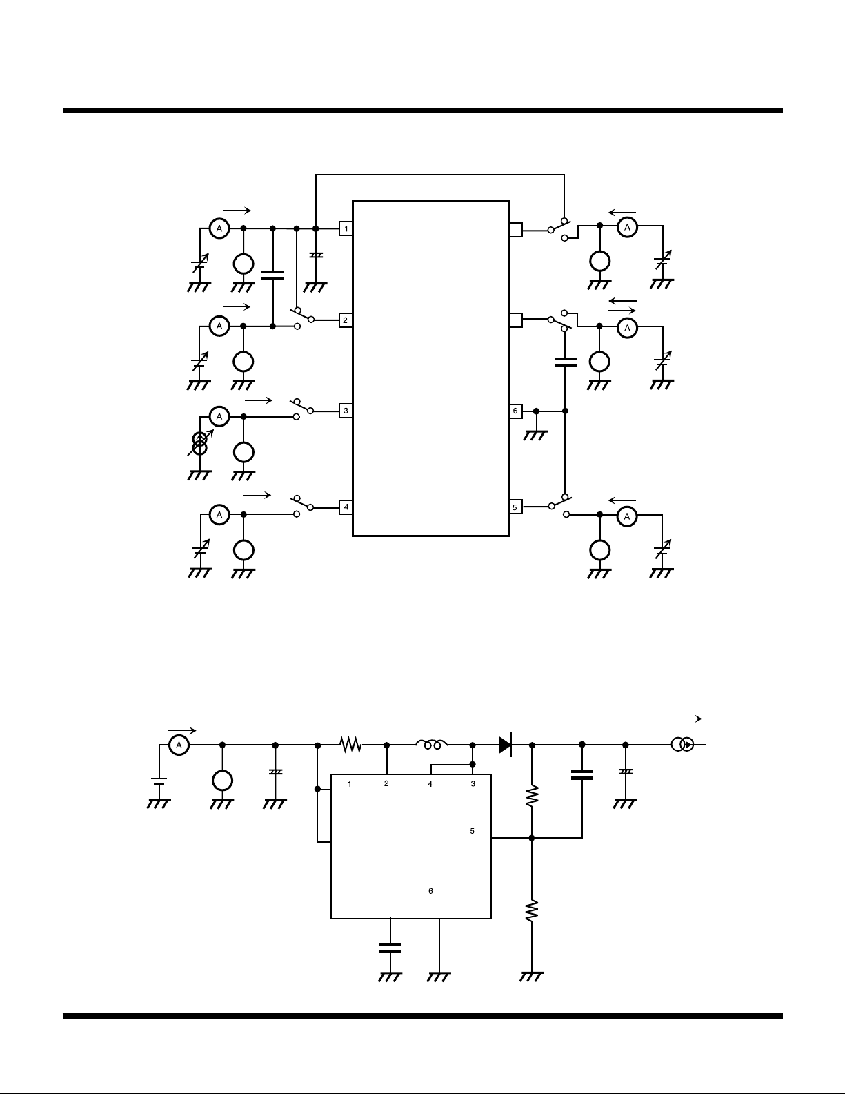
TEST CIRCUIT
I
CC
V
IN
V
V
IN
I
IS
I
EXT
I
VOUT
IN
V
V
IS
V
V
EXT
V
V
OUT
V
V V
10 µF
I
S
EXT
V
OUT
EN
C
GND
V
FB
X
8
7
100 pF
V
EN
V
V
CX
V
V
FB
I
EN
I
DIS
I
CHG
I
FB
REFERENCE DATA TEST CIRCUIT
I
C
47µ
LOAD
20 mA
OUT
I
CC
3.6 V
R
SC
0.22Ω
V
IN
V
C
47µ
IN
V
8
EN
IN
C
X
56 pF
I
TK11850L
C
L
15µ
V
S
OUT
7
GND
X
EXT
V
FB
D
620k
20k
V
2200p
L = 15 mH D52LC (A914BYW - 150M) Toko
D - SB07 - 03C Sanyo
OUT
Page 4 May 2001 TOKO, Inc.

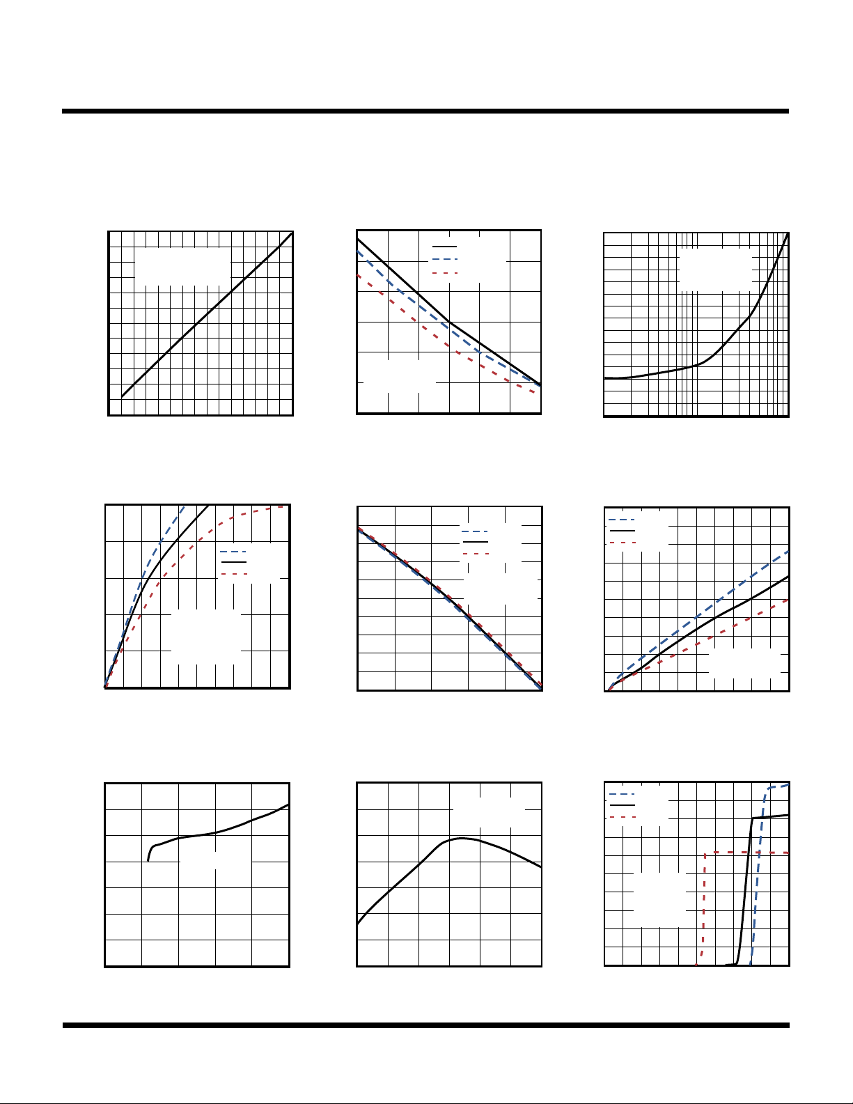
TYPICAL PERFORMANCE CHARACTERISTICS
SUPPLY CURRENT (mA)
10
SUPPLY CURRENT vs.
EN VOLTAGE
EN VOLTAGE (V)
0 0.2 0.4 0.6 0.8 1 1.2 1.4 1.6 1.8 2
9
8
7
6
5
4
3
2
1
0
-20 °C
25 °C
85 °C
VIN = 3 V
VIS = V
IN
VFB = 0 V
CX = 100 pF
TA = 25 °C, unless otherwise specified.
TK11850L
OSC PERIOD vs. C
CAPACITANCE
12
11
10
9
VIN = 3 V
VIS = VEN = V
IN
8
7
6
5
4
OSC PERIOD (µS)
3
2
1
0
0 100 200 300
CX CAPACITANCE (pF)
SWITCHING CURRENT vs.
SWITCH SATURATION VOLTAGE
500
400
300
200
100
VIN = 3 V
VIS = VEN = V
VFB = 0 V
VCX = 0 V
IN
SWITCHING CURRENT (mA)
0
0 0.1 0.2 0.3 0.4 0.5 0.6 0.7 0.8 0.9 1
SWITCH SATURATION
VOLTAGE (V)
X
-20 °C
25 °C
85 °C
OSC FREQUENCY vs.
TEMPERATURE
300
280
VIN = 3 V
V
VIN = 10 V
260
240
220
VIS = VEN =V
CX = 100 pF
200
OSC FREQUENCY (kHz)
180
-30 -10 10 30 50 70 90
IN
TEMPERATURE (°C)
INDUCTOR CURRENT-LIMIT SENSE
VOLTAGE vs. SUPPLY VOLTAGE
100
90
80
70
60
50
40
30
20
SENSE VOLTAGE (mV)
INDUCTOR CURRENT-LIMIT
10
0
2 4 6 8 10 12
SUPPLY VOLTAGE (V)
IN = 5 V
V
limit
VEN = V
-20 °C
25 °C
85 °C
= VIS - V
IN
MAXIMUM DUTY CYCLE vs.
OSC FREQUENCY
80
VIN = 3 V
VIS = V
EN = VIN
VFB = 0 V
75
70
MAXIMUM DUTY CYCLE (%)
65
10 100 1000
OSC FREQUENCY (kHz)
IS INPUT BIAS CURRENT
vs. IS VOLTAGE
100
90
80
-20 °C
25 °C
85 °C
70
IN
60
50
40
30
20
INPUT BIAS CURRENT (µA)
10
S
I
0
0 2 4 6 8 10 12 14 16 18 20
VIN = VEN = V
VFB = 1 V
IS
IS VOLTAGE (V)
REFERENCE VOLTAGE vs.
SUPPLY VOLTAGE
530
528
526
524
522
520
518
REFERENCE VOLTAGE (mV)
516
0 2 4 6 8 10
SUPPLY VOLTAGE (V)
May 2001 TOKO, Inc. Page 5
VIS = VEN = V
REFERENCE VOLTAGE vs.
TEMPERATURE
530
528
VIN = 3 V
VIS = VEN = V
IN
526
IN
524
522
520
518
REFERENCE VOLTAGE (mV)
516
-30 -10 10 30 50 70 90
TEMPERATURE (°C)
 Loading...