TOKO TK11823MBX, TK11823MTL, TK11822MTL, TK11822MBX Datasheet

TK11822/11823
1
2
3
4
EMITTER
BASE
DA V
O
6
5
V
IN
GND
E
T
DC-DC CONVERTER
FEATURES
■ Very Low Noise
■ Low Operating Voltage Range
■ Few External Components
■ Wide Supply Voltage Range
■ Sinewave Oscillation
■ Selectable Output Voltages
DESCRIPTION
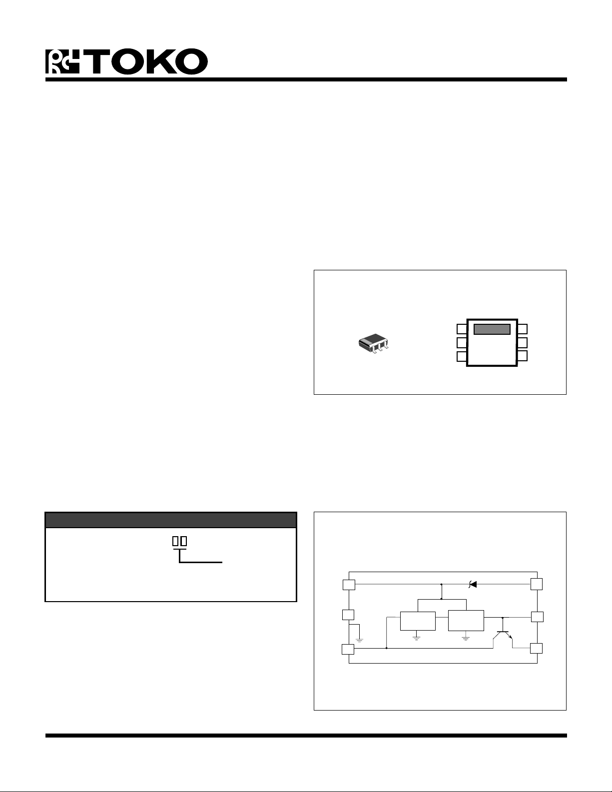
The TK11822M and TK11823M are booster-type DC-DC
converters developed principally for use as power supplies
to drive variable capacitance diodes. Both products are low
power output types, suitable for operation at low voltages.
To suppress AM band noise, they use high frequency sine
wave oscillation. Both products are available in two output
voltages, allowing the user to select the most efficient
voltage for the equipment. The products have built-in rectifier diodes and small packages, contributing to equipment
miniaturization.
APPLICATIONS
■ Headphone Stereos
■ Pagers
■ Mobile Wireless Equipment
■ Electronic Diaries
■ Other Battery-powered Equipment
■ LCD TV's
TK11822/23M
R3
March 19, 1996 TOKO, Inc.
ORDERING INFORMATION
TK11822M
TK11823M
TAPE/REEL CODE
BX: Bulk/Bag
TL: Tape Left
Tape/Reel Code
V
O
GND 5
VIN 6
BLOCK DIAGRAM
4
Reference
Voltage
Feedback
Control
3 DA
2 BAS
1 EMIT
Page 1

TK11822/11823
ABSOLUTE MAXIMUM RATINGS
Input Voltage.............................................................. 8 V
Output Current ..................................................... 0.5 mA
Operating Voltage Range................................. 1.1 to 6 V
Power Dissipation (Note 1) ................................ 200 mW
TK11822 ELECTRICAL CHARACTERISTICS
Test conditions: V
SYMBOL PARAMETER TEST CONDITIONS MIN TYP MAX UNITS
I
CC
V
O
I
O
Line Reg Line Regulation VIN = 1.4 V → 3.6 V, IO = 50 µA2080mV
Load Reg Load Regulation IO = 20 µA → 100 µA 30 100 mV
= 1.4 V, TA = 25 °C, unless otherwise specified.
IN
Input Current
IO = 0 µA 2.1 3.6 mA
IO = 50 µA 3.8 5.6 mA
Output Voltage IO = 50 µA 7.0 7.4 7.8 V
Output Current
VIN = 1.2 V 50 µA
VIN = 1.4 V 150 µA
Junction Temperature .......................................... 150 °C
Storage Temperature Range ...................-55 to +150 °C
Operating Temperature Range .................-20 to +70 °C
Lead Soldering Temp. (10 sec.)...........................260 °C
∆VO/T
A
Output Voltage VIN = 1.4 V → 3.6 V, IO = 50 µA 0.7 mV/°C
Temperature Dependency
V
OSC-S
f
OSC
Note 1: Power dissipation must be derated at the rate of 1.6 mW/°C for operation above 25 °C.
Note 2: Use caution when decreasing the output capacitance at low temperatures. "UJ" type capacitors will allow little change in
the oscillation frequency.
Oscillation Startup Voltage IO = 0 µA 1.0 V
Oscillation Frequency 3.0 MHz
TEST CIRCUIT
GND
V
V
0.1 µF
0.1 µF
IN
O
4
+
5
+
6
3
5 pF
2
8 pF
1
C1
6
1
4
3
Page 2
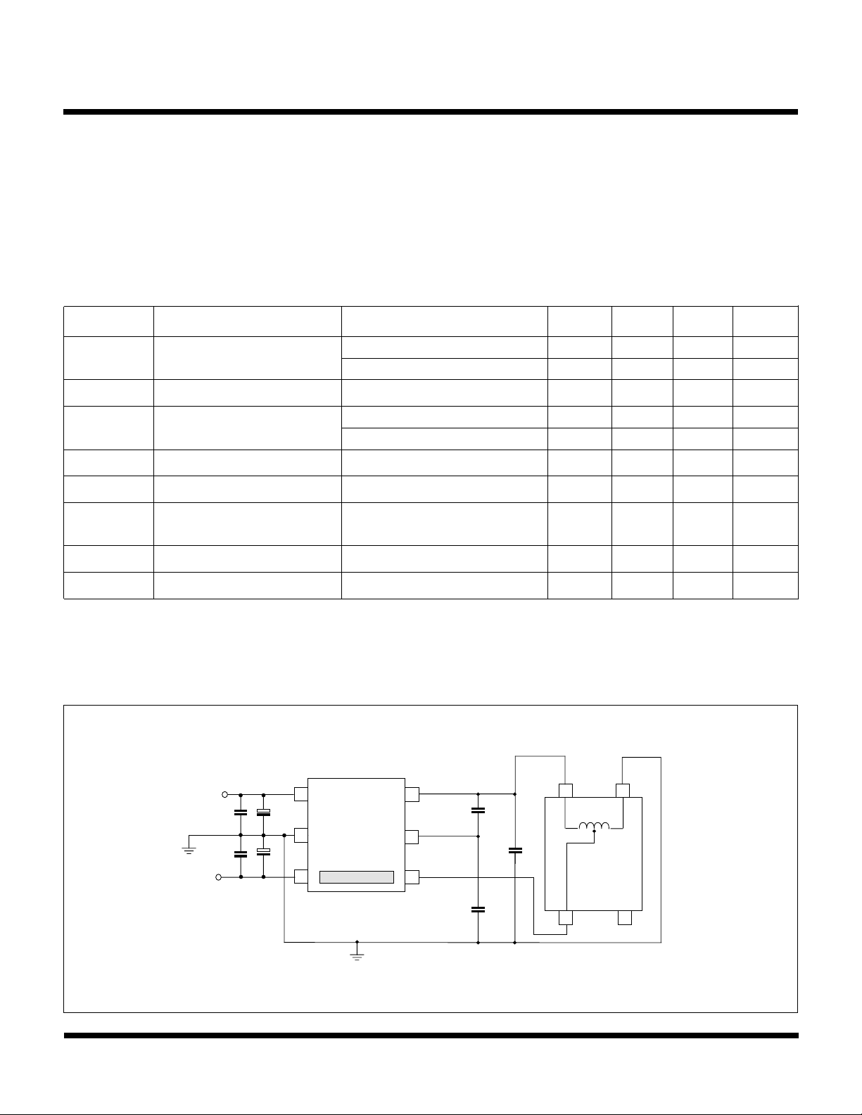
Toko Inductor: 5CDM-658BN-1085
TK11822 C1 33 pF
TK11823 C1 68 pF
March 19, 1996 TOKO, Inc.
 Loading...