TOKO TK11819MTL, TK11818MTL, TK11817MTL, TK11816MTL Datasheet

TK11816, TK11817,
01S
TK11818, TK11819
DC-DC CONVERTER
FEATURES
■ Miniature Package (SOT-23L-6)
■ Few External Components
■ Internal Rectifier and Regulator
■ Wide Input Voltage Range (1.1 to 18 V)
■ Selectable Output Voltages
■ Single Battery Cell Operation
DESCRIPTION
The TK1181x series devices generate DC output voltages
ranging from 7.2 to 32 V. Each device provides two
regulated output voltages selectable by a single jumper.
Designed for step-up operation, these devices will operate
with an input voltage as low as 1.1 V, thus allowing single
battery cell operation.
These converters have a built-in relaxation oscillator. The
frequency of operation is determined by external component
values. The built-in rectifier combined with an internal
temperature compensated reference allows stable output
voltages with minimal external components.
APPLICATIONS
■ Variable Capacitance and PIN Diode Bias
■ Portable Instrumentation
■ Radio Control Systems
■ Mobile Radios
■ Cellular Telephones
■ Cordless Telephones
■ Fiber-Optic Receivers
■ Local Area Network (LAN) Receivers
■ Battery Operated Equipment
TK11816 TK11817
TK11818 TK11819
V
IN
OSC
DK
T
1
GND
V
OUT
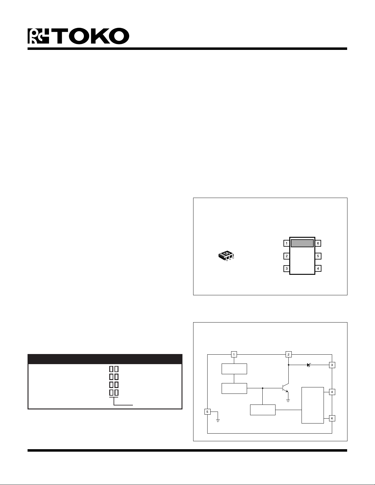
These devices are available in a miniature SOT-23L-6
surface mount package. An optimized surface mount
inductor is available from TOKO (P/N: 395GN-0091IB).
BLOCK DIAGRAM
OSCV
DK
ORDERING INFORMATION
TK11816M
IN
STARTUP
CIRCUIT
TK11817M
TK11818M
TK11819M
Tape/Reel Code
TAPE/REEL CODE
TL: Tape Left
January 1999 TOKO, Inc. Page 1
GND
OSCILLATOR
FEEDBACK
CONTROL
REFERENCE
VOLTAGE
V
OUT
T
1

TK11816, TK11817,
TK11818, TK11819
ABSOLUTE MAXIMUM RATINGS
Input Voltage ............................................................20 V
Power Dissipation (Note 1) ................................200 mW
Junction Temperature .......................................... 150 °C
Operating Voltage Range (TK11816).............1.1 to 13 V
Operating Voltage Range (TK11817).............1.1 to 15 V
Operating Voltage Range (TK11818).............1.1 to 18 V
Operating Voltage Range (TK11819).............1.1 to 18 V
Storage Temperature Range ...................-55 to +150 °C
Operating Temperature Range ..................-20 to +70 °C
Lead Soldering Temperature (10 s) .................... 235 °C
TK11816 ELECTRICAL CHARACTERISTICS
Test Conditions: VIN = 5 V, TA = 25 °C (Notes 3 & 5), unless otherwise specified.
LOBMYSRETEMARAPSNOITIDNOCTSETNIMPYTXAMSTINU
I
V
I
∆V
V
NI
tnerruCylppuS
TUO
V
TUO
V1.1 ≤ VNI≤ V011.218.215.31V
TUO
TUO
egatloVtuptuO
V1.1 ≤ VNI≤ V658.602.705.7V
V
tnerruCtuptuO
TUO
V
TUO
geRdaoLnoitalugeRdaoL)4etoN(60.03.0%
V
TUO
/∆T
tneiciffeoCerutarepmeT
TUO
V
TUO
,V8.21=I
TUO
,V2.7=I
TUO
Am1.0=7.40.9Am
Am0.1=1.210.91Am
V8.21=5.35.4Am
V2.7=0.40.6Am
,V8.21=I
TUO
,V2.7=I
TUO
Am1.0=10.1C°/Vm
Am1.0=20.2C°/Vm
TK11817 ELECTRICAL CHARACTERISTICS
Test Conditions: VIN = 5 V, TA = 25 °C (Notes 3 & 5), unless otherwise specified.
LOBMYSRETEMARAPSNOITIDNOCTSETNIMPYTXAMSTINU
V
I
NI
tnerruCylppuS
TUO
V
TUO
V1.1 ≤ VNI≤ V510.618.616.71V
V
TUO
I
TUO
egatloVtuptuO
V1.1 ≤ VNI≤ V858.803.908.9V
V
tnerruCtuptuO
TUO
V
TUO
geRdaoLnoitalugeRdaoL)4etoN(60.03.0%
V
∆V
TUO
/∆T
tneiciffeoCerutarepmeT
TUO
V
TUO
Page 2 January 1999 TOKO, Inc.
,V8.61=I
TUO
,V3.9=I
TUO
Am1.0=7.40.9Am
Am0.1=1.210.91Am
V8.61=5.35.4Am
V3.9=0.40.6Am
,V8.61=I
TUO
,V3.9=I
TUO
Am1.0=18.1C°/Vm
Am1.0=13.2C°/Vm

TK11818 ELECTRICAL CHARACTERISTICS
Test Conditions: VIN = 5 V, TA = 25 °C (Notes 3 & 5), unless otherwise specified.
LOBMYSRETEMARAPSNOITIDNOCTSETNIMPYTXAMSTINU
TK11816, TK11817,
TK11818, TK11819
V
I
NI
tnerruCylppuS
TUO
V
TUO
,V82=I
TUO
,V4.02=I
TUO
Am1.0=7.40.9Am
Am0.1=1.210.91Am
V1.1 ≤ VNI≤ V814.620.826.92V
V
TUO
I
TUO
egatloVtuptuO
V1.1 ≤ VNI≤ V813.914.025.12V
tnerruCtuptuO
V
V
V82=8.10.3Am
TUO
TUO
V4.02=5.20.4Am
geRdaoLnoitalugeRdaoL)4etoN(60.03.0%
∆V
TUO
/∆T
V
tneiciffeoCerutarepmeT
TUO
V
TUO
,V82=I
TUO
,V4.02=I
TUO
Am1.0=2.0C°/Vm
Am1.0=6.0C°/Vm
TK11819 ELECTRICAL CHARACTERISTICS
Test Conditions: VIN = 5 V, TA = 25 °C (Notes 3 & 5), unless otherwise specified.
LOBMYSRETEMARAPSNOITIDNOCTSETNIMPYTXAMSTINU
V
I
NI
tnerruCylppuS
TUO
V
TUO
V1.1 ≤ VNI≤ V810.030.230.43V
V
TUO
egatloVtuptuO
V1.1 ≤ VNI≤ V815.220.425.52V
,V23=I
TUO
,V42=I
TUO
Am1.0=7.40.9Am
Am0.1=1.210.91Am
I
TUO
tnerruCtuptuO
V
V
V23=8.10.3Am
TUO
V42=5.20.4Am
TUO
geRdaoLnoitalugeRdaoL)4etoN(60.03.0%
V
∆V
/∆T
TUO
Note 1: Power dissipation is 400 mW when mounted. Derate at 3.2 mW/°C for operation above 25 °C. Power dissipation is 200 mW in free air. Derate
Note 2: When operating below 25 °C, the output capacitor degradation may increase output ripple noise.
Note 3: VIN = 5.0 V, No load.
Note 4: Load Regulation = (∆V
Note 5: Specifications are based upon a Toko 395GN-0091IB inductor. The use of other inductors may degrade performance.
Note 6: See Output Voltage Selection Table for connections to obtain desired output voltage.
at 1.6 mW/°C for operation above 25 °C.
/ V
OUT
tneiciffeoCerutarepmeT
) x 100 %, where ∆V
OUT
TUO
V
TUO
= V
OUT
,V23=I
,V42=I
(no load) - V
OUT
TUO
TUO
Am1.0=19.0C°/Vm
Am1.0=73.1C°/Vm
OUT (IOUT
= 1.0 mA)
January 1999 TOKO, Inc. Page 3
 Loading...