TOKO TK11806MTL, TK11806MMG, TK11806MBX Datasheet

TK11806
C
G
V
A
3
2
1
DC-DC CONVERTER
FEATURES
■ Very Small Size
■ Few External Components
■ Wide Input Supply Voltage Range (1.1 to 18 V)
■ Six Selectable Output Voltages up to 32 V
■ Single Battery Cell Operation
DESCRIPTION
The TK11806 is a low power, low input voltage DC-DC
converter.
The device has been optimized for variable capacitance
diode and PIN diode bias applications. It generates DC
output voltages ranging from 9.3 V to 32 V in six steps. The
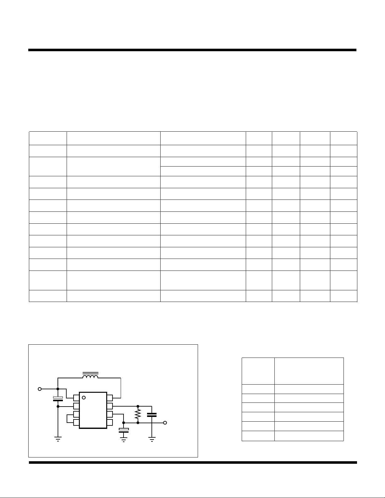
desired output voltage may be selected by simple wire
connections between control pins. The input DC voltage
can be as low as 1.1 V or as high as 18 V.
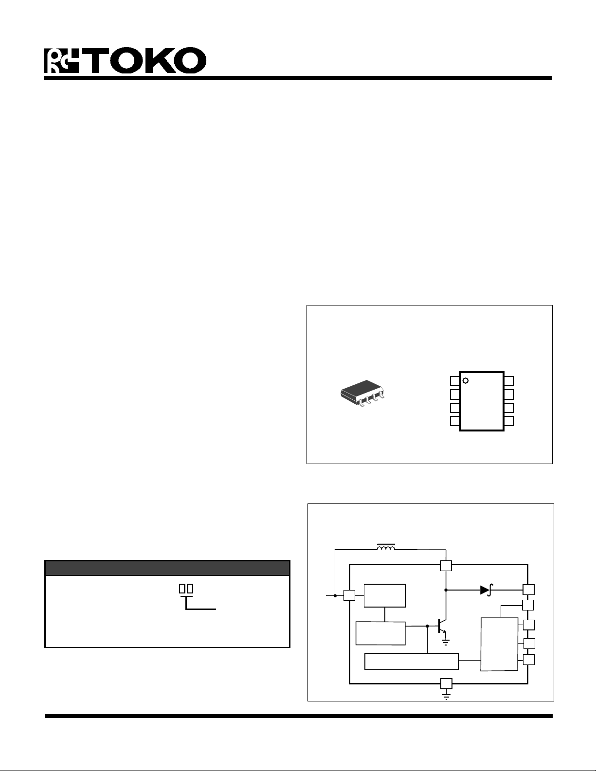
The device has a built-in relaxation oscillator. The frequency of oscillation is determined by external component
values. The TK11806 has built-in voltage reference and an
array of temperature compensated zener diodes in order to
generate various output voltages with minimum external
part count.
APPLICATIONS
■ Variable Capacitance and PIN Diode Bias
■ Portable Instrumentation
■ Radio Control Systems
■ Mobile Radios
■ Cellular Telephones
■ Cordless Telephones
■ Fiberoptic Receivers
■ Local Area Network (LAN) Receivers
■ Battery Operated Equipment
TK11806M
V
1
806
A21
IN
2
ND DA
3
T1
T2
4
8
OS
7
V
6
O
5
T3
The device is available in an 8-lead plastic surface mount
package (MFP-8).
External inductive components are also available from
TOKO.
ORDERING INFORMATION
TK11806M
Tape/Reel Code
January, 1996 TOKO, Inc.
TAPE/REEL CODE
BX: Bulk/Bag
TL: Tape Left
MG: Magazine
1-16-96
S
1
IN
BLOCK DIAGRAM
L
EXT
STARTUP
CIRCUIT
OSCILLATOR
FEEDBACK
CONTROL
OSC.
8
S
S
REF.
VOLTAGE
2
GND
7
D
V
6
O
T
5
T
4
3
T
Page 1

TK11806
V
V
TOKO P/N : 395AN-0091B
ABSOLUTE MAXIMUM RATINGS
Input Voltage ............................................................ 20 V
Output Voltage ......................................................... 35 V
Power Dissipation (Note 1) ................................ 350 mW
Junction Temperature ...........................................150 °C
ELECTRICAL CHARACTERISTICS
Test conditions: V
SYMBOL PARAMETER TEST CONDITIONS MIN TYP MAX UNITS
= 5.0 V, V
IN
= 32.0 V, TA = 25 °C, IO = 0 µA, unless otherwise specified.
O
Storage Temperature Range ................... -55 to +150 °C
Operating Temperature Range ...................-20 to +70 °C
Lead Soldering Temp. (10 sec.) M-Package.........260 °C
V
IN
I
IN
V
O1
V
O2
V
O3
V
O4
V
O5
V
O6
I
O
Supply Voltage Range 1.1 18 mA
Supply Current
IO = 0.1 mA 4.7 90 mA
IO = 0.1 mA
12.1 19 µA
Output Voltage 1.1 V≤VIN≤18.0 V, Note 2 30 32.0 34 V
Output Voltage 1.1 V≤VIN≤18.0 V, Note 2 26 28 30 V
Output Voltage 1.1 V≤VIN≤18.0 V, Note 2 22.0 24.0 26.0 V
Output Voltage 1.1 V≤VIN≤18.0 V, Note 2 15.5 16.8 18.0 V
Output Voltage 1.1 V≤VIN≤18.0 V, Note 2 11.0 12.8 14.5 V
Output Voltage 1.1 V≤VIN≤18.0 V, Note 2 8.0 9.3 10.5 V
Output Current Note 3 1.8 2.4 mA
Load Reg Load Regulation IO = 0.0 mA → 1.0 mA .24 0.5 %
∆VO/∆T
Output Voltage IO = 0.1 mA 0.25 mV/ °C
A
Temperature Dependency
V
OSC
Note 1: Power dissipation must be derated at the rate of 3 mW/°C for operation at TA = 25 °C and above.
Note 2: Connect T
Note 3: Use inductor as specified.
Oscillator Start-up Voltage IO = 0 mA 0.9 1.1 V
through T3 as specified.
1
TEST CIRCUIT
OUTPUT
1.2 mH
IN
Page 2
22
µF
S
+
1
S
2
T1
3
4
T2
8
7
6
TK11806M
5
T3
820 W
+
10 µF
S
0.2 µF
V = 32
O
KT11806• TC01
1-16-96
SS
VOLTAGE CONNECTION
(V)
32 T
28 T1-T
24 T1-T2-T
17 T1-T2 , T3-V
13 T1-V
9.3 T1-T2-V
1-T2
3
3
O
O
O
January, 1996 TOKO, Inc.

TYPICAL PERFORMANCE CHARACTERISTICS
5
1
0
7
V
TK11806
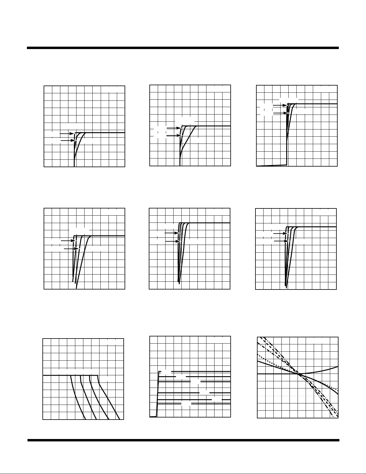
OUTPUT VOLTAGE vs. INPUT VOLTAGE
VO = 9.3 V
20
400 µA
800 µA
IO = 0 µA
1200 µA
O
10
V (V)
0
0 0.5 1.0 1.5 2.0 2.
V (V)
IN
OUTPUT VOLTAGE vs. INPUT VOLTAGE
VO = 24 V
30
IO = 0 µA
200 µA
O
20
V (V)
400 µA
600 µA
TA = 25 °C
TK11806 • TPC0
TA = 25 °C
OUTPUT VOLTAGE vs. INPUT VOLTAGE
VO = 13 V
20
IO= 0 µA
O
400 µA
10
V (V)
800 µA
1200 µA
0
0 0.5 1.0 1.5 2.0 2.5
V (V)
IN
OUTPUT VOLTAGE vs. INPUT VOLTAGE
VO = 28 V
30
IO = 0 µA
100 µA
O
20
V (V)
200 µA
300 µA
TA = 25 °C
TK11806 • TPC02
TA = 25 °C
OUTPUT VOLTAGE vs. INPUT VOLTAGE
VO = 17 V
20
IO = 0 µA
200 µA
600 µA
O
10
V (V)
400 µA
0
0 0.5 1.0 1.5 2.0 2.5
V (V)
IN
OUTPUT VOLTAGE vs. INPUT VOLTAGE
VO = 32 V
35
IO = 0 µA
100 µA
O
25
V (V)
200 µA
300 µA
TA = 25 °C
TK11806 • TPC03
TA = 25 °C
10
0 0.5 1.0 1.5 2.0 2.5
V (V)
IN
OUTPUT VOLTAGE vs. OUTPUT CURRENT
VO = 32 V
40
4.5 V 5.5 V
O
V (V)
V = 3.5 V
IN
30
20
0 1.0 2.0 3.0 4.0 5.
I (mA)
O
January, 1996 TOKO, Inc.
TK11806 • TPC04
TA = 25 °C
6.5 V
TK11806 • TPC0
10
0 0.5 1.0 1.5 2.0 2.5
V (V)
IN
TK11806 • TPC05
OUTPUT VOLTAGE vs. INPUT VOLTAGE
50
32 V
O
V (V)
25
28 V
24 V
9.3 V
0
0246810
V (V)
IN
1-16-96
TA = 25 °C
17 V
13 V
TK11806 • TPC08
15
0 0.5 1.0 1.5 2.0 2.5
V (V)
IN
TK11806 • TPC06
OUTPUT VOLTAGE DRIFT vs.
TEMPERATURE
100
0
OUT
∆V (mV)
-100
-20 0 +20 +40 +60 +80
IO = 500 µA
TA (°C)
17 V
TK11806 • TPC09
Page 3
28 V
24 V
32 V
13 V
9.3
 Loading...