

TMI TAMARACK TC5299J Datasheet

TC5299J
TC5299J
FAST ETHERNET PCMCIA
LAN CONTROLLER
4FL No. 106 Hsin-Tai Wu Road,
Sec. 1, Hsichih,
Taipei Hsien, Taiwan R.O.C.
TEL: 886-2-2696-1669
FAX: 886-2-2696-2220
http:\\www.tmi.com.tw
-1-
Ver. 0.1
07/04/01

TC5299J
TABLE OF CONTENTS
1 Introduction .................................................................................................................................3
1.1 General Description.............................................................................................................................................3
1.2 Features...............................................................................................................................................................3
2 Block Diagram .............................................................................................................................3
3 Pin Description.............................................................................................................................4
3.1 Pin Out Diagram .................................................................................................................................................4
3.2 Signal Description...............................................................................................................................................5
3.3 Power On Configuration.....................................................................................................................................8
4 I/O and Mapping .......................................................................................................................10
4.1 I/O Port Address Mapping................................................................................................................................10
4.2 EEPROM/SRAM Memory Mapping................................................................................................................10
4.3 Attribute Memory Mapping..............................................................................................................................11
4.3.1 Attribute Memory Map......................................................................................................................11
5 Configuration Registers ............................................................................................................13
5.1 Configuration Register A..................................................................................................................................13
5.2 Configuration Register B ..................................................................................................................................13
5.3 Configuration Register C ..................................................................................................................................14
5.4 Hardware Configuration....................................................................................................................................14
5.5 MII/PHY Control Register................................................................................................................................15
5.6 TC5299J Core Registers Assignment................................................................................................................15
5.7 Register Descriptions........................................................................................................................................18
5.7.1 Command Register (CR) 00H (Read/Write)......................................................................................18
5.7.2 Data Configure register (DCR) 0EH(Write)....................................................................................19
5.7.3 Transmit configuration Register (TCR) 0DH(Write) ........................................................................19
5.7.4 Transmit Status Register (TSR) 04H(Read).....................................................................................20
5.7.5 Receive Configuration Register (RCR) 0CH(Write)........................................................................21
5.7.6 Receive Status Register (RSR) 0CH(Read)......................................................................................21
5.7.7 Interrupt Mask Register (IMR) 0FH(Write)....................................................................................22
5.7.8 Interrupt Status Register (ISR) 07H(Read/Write)............................................................................23
5.8 Network Tally Counter Registers (CNTR)........................................................................................................23
5.9 Number of Collisions Register (NCR)..............................................................................................................24
5.10 Physical Address Register (PAR0-PAR5).........................................................................................................24
5.11 Multicast Address Registers (MAR0-MAR7)...................................................................................................24
5.12 DMA Registers..................................................................................................................................................25
5.13 LOCAL DMA RECEIVE REGISTERS...........................................................................................................25
5.14 REMOTE DMA REGISTERS..........................................................................................................................25
5.15 (i) Local DMA Transmit Registers ............................................................................................... ....................25
5.16 (ii) Local DMA Receive Registers....................................................................................................................26
5.17 (iii) Remote DMA registers...............................................................................................................................26
6 Electrical Specification and Timing.........................................................................................28
7 Physical Dimension....................................................................................................................31
Notice.................................................................................................................................................32
-2-
Ver. 0.1
07/04/01
Fast Ethernet PCMCIA Controller
1 Introduction
1.1 General Description
The TC5299J is a 10/100 PCMCIA Ethernet controller, include a standard MII interface. It provides an 8/16-bit
PCMCIA interface to host CPU and buffer memory into single chip to minimize the chip gate count.
The TC5299J supports both half-duplex and full-duplex (both 10BT or 100BTX) operation environment.
1.2 Features
!"PCMCIA 2.01 bus interface.
!"Use serial EEPROM 93C56/66 to store CIS.
!"Internal 5V to 3.3V regulator.
Ethernet LAN features:
!"Integrated Fast Ethernet MAC and SRAM in one chip.
!"Supports both 10Mbps and 100Mbps operation.
!"IEEE 802.3/802.3u compatible.
!"Full-duplex or half-duplex operation supported for both 10Mbps and 100Mbps operation.
!"NE2000 register definitions.
!"Supports 3.3V or 5V signaling environment.
!"The size of built-in Buffer RAM is 8k x 16 bits. It does not need the extra SRAM in the application circuit.
!"Supports loop-back mode for self-testing.
!"Supports 256/512 bytes EEPROM interface.
!"LED interface supported.
!"Supports MII bus interface.
!"Flow control ability
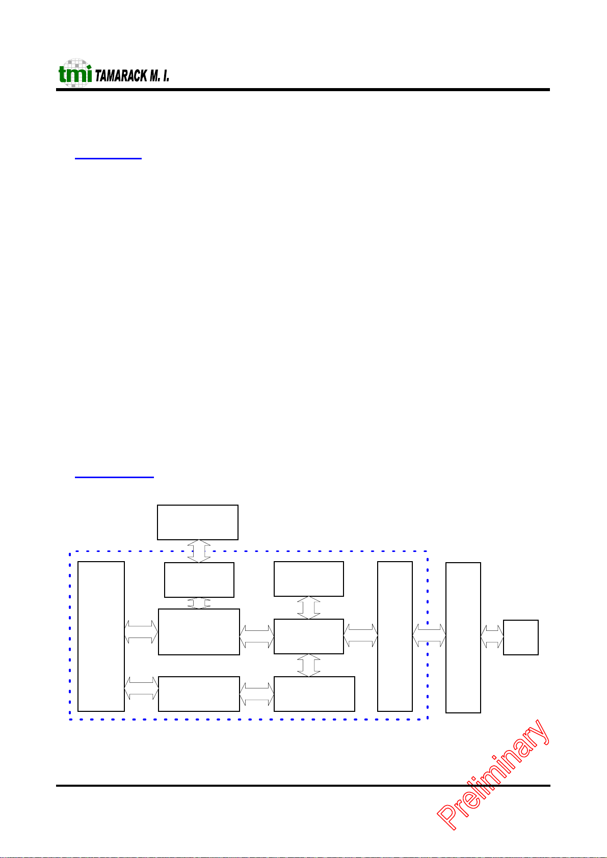
2 Block Diagram
TC5299J
PCMCIA
Inte r fa c e
EEPROM
EEPROM
Control Circuit
PCMCIA
Command
Decoder
DMA Buffer
Control Logic
SRAM
FIFOs
FIFO
Controller
-3-
MAC
PHY
TW R
RJ45
Ver. 0.1
07/04/01

3 Pin Description
3.1 Pin Out Diagram
TC5299J
NC
NC
GNDAT
VCCAT
VCC5A
VCC5R
NC
VCC3IO
RSTN
GND3IO
JMP0
GND3D
GND3IO
JMP1
NC
VCC3D
VCC3IO
SD15
SD14
SD13
SD12
GND3IO
SD11
SD10
VCC3D
SD9
SD8
VCC3IO
INT
IOR
OE
GND3IO
G
N
V
V
C
C
C
C
5
A
N
N
C
R
C
234567891011121314151617181920212223242526272829303132
97
98
99
100
101
102
103
104
105
106
107
108
109
110
111
112
113
114
115
116
117
118
119
120
121
122
123
124
125
126
127
128
A
1
G
G
D
N
N
A
D
D
1
A
A
0
P
R
128pin LQFP
V
G
C
V
N
D
D
P
V
C
C
C
A
C
C
1
D
A
N
0
P
C
P
C
V
G
C
N
C
3
IONCNCN
G
D
N
3
D
ION
3
C
D
G
N
M
D
D
3
I
NCN
C
D
O
TC5299J
V
L
C
E
E
C
L
E
D
C
L
S
A
L
3
E
E
I
D
D
O
S
F
G
N
D
3
I
O
G
N
D
3
IOX1X
2
6566676869707172737475767778798081828384858687888990919293949596
64
63
62
61
60
59
58
57
56
55
54
53
52
51
50
49
48
47
46
45
44
43
42
41
40
39
38
37
36
35
34
33
VCC3D
VCC5A
VCC5R
VCC5A
VCC3IO
MDC
RXD3
RXD2
GND3IO
RXD1
RXD0
X25M
RXDV
RXC
RXER
GND3IO
TXC
TXEN
TXD0
TXD1
GND3IO
TXD2
TXD3
GND3D
COL
CRS
VCC3IO
EXLEDF
EXLEDL
CE1
WE
NC
S
S
S
S
S
S
S
S
S
S
S
S
S
S
I
S
S
S
V
O
A
C
W
9
C
3
I
O
G
A
A
A
A
N
8
7
D
3
D
A
6
5
4
S
A
A
A
3
2
1
NCR
G
A
N
0
D
3
I
O
I
W
E
N
S
A
G
P
T
I
A
T
C
K
D
O
N
0
I
D
S
3
1
I
6
O
I
R
G
V
D
D
C
1
2
C
3
I
O
V
D
3
D
D
C
5
4
C
3
D
G
D
D
N
6
7
D
3
I
O
-4-
Ver. 0.1
07/04/01

3.2 Signal Description
PCMCIA Bus Interf ace Pins
Symbol Pin # I/O Description
SA[9:0] 3-5
7-12,
14
SD[15:8]
SD[7:0]
RST 16 I/O RST is active high and places the TC5299J in a reset mode
RSTZ 105 O RSTZ is an active low signal. It is an inverted signal of RST.
WAIT* 17 O This pin is set low to insert wait states during Remote DMA
REG* 19 I REG is an active low input used to determine whether a host
IOR* 126 I Read Strobe: Strobe from host to read registers or Remote DMA
IOW* 2 I Write Strobe: Strobe from host to read registers or Remote DMA
OE* 127 I Host memory read strobe, when OE* and REG* both low the
WE* 34 I Host memory write strobe, After Power reset if TC5299J is
INPACK* 18 O An active low signal. Asserted if the host access register or
IO16* 21 O IO16* is driven by TC5299J to support host 16 bits access cycle.
INT*
(RDY/BSY*)
CE1* 35 I Card enable 1, is active low signals driven by the host. This
114-117,
119-120,
122-123,
31-29,
27-26,
24-22
125 O While the TC5299J is configured as a memory device, this pin
I The address signal lines of PCMCIA Bus are used to select a
register to be read or written and attribute memory enabled.
I/O Register Access, with DMA inactive, SD0-SD7 are used to
read/write register data. SD8-SD15 invalid during this state.
Remote DMA Bus Cycle, SD0-SD15 contain packet data.
Direction of transfer depends on Remote read/write.
immediately. During falling edge the TC5299J controller loads
the configuration from JMP0 – JMP8.
transfer.
access is to Attribute memory or to common memory. If REG is
low the access is to attribute memory, if REG* is high the access
is to common memory. REG* is also asserted low for all accesses
to the TC5299J IO Registers.
read.
write.
attribute memory can be read. When OE* is low and REG* is
high common memory can be read .
configured to memory write enable, then WE and REG* is both
low, Attribute memory can be written. When WE is low and
REG* is high common memory can be written.
Remote DMA read cycle.
servers as RDY/BSY* pin, If the TC5299J is ready to perform a
transfer, this pin is set high. When TC5299J is operated at I/O
mode, this pin is used as an interrupt pin. It indicates that the
TC5299J needs host service. RDY/BSY* state can be read from
the pin Replacement Register (CCR2). While LAN and MODEM
both functions are enabled and IntSel bit in control Register
(CCR5) is zero. This pin output is logical OR of LAN and
MODEM interrupt.
signal provides a card select based on the address decode (decode
by the host).
TC5299J
-5-
Ver. 0.1
07/04/01

EEPROM/LED Inter fa ce Pins
Symbol Pin # I/O Description
EECS 73 O EEPROM chip select. It is asserted when to access EEPROM.
EESK/LED LA 72 O Link (on/off) & Re ce i ve d a ta ( B link) LE D p i n. I t i s al so use d as a
serial clock for EEPROM data loading.
DO/LEDS 70 I/O Speed (100M:ON/10M:OFF) & transmit data (Blink) LED pin. It
is also used as a signal for EEPROM data loading.
DI/LEDF 69 O Full-duplex (ON/OFF, Full/Half-duplex) & Collision (Blink)
LED pin. It is a data output pin for EEPROM writing.
External PHY / MII Interface Pins
Symbol Pin # I/O Description
TXD[3:0] 42-43,
45-46
TXEN 47 I/O This pin function as transmit enable. It indicates that a
TXC 48 I Supports the transmit clock supplied by the external PMD device.
RXD[3:0] 58-57,
55-54
RXC 51 I Supports receive clock from PHY. And is recovered by the PHY.
RXDV 52 I Data valid is asserted by an external PHY when receive data is
RXER 50 I Data valid is asserted by an external PHY when receive data is
COL 40 I This pin functions as the collision detect. When the external
CRS 39 I In MII mode this pin functions as the carrier sense and is asserted
MDC 59 O MII management data clock is sourced by the TC5299J to the
MDIO 74 I/O MII management data input/output transfers contro l information
EXLEDL 36 I Low active; presents the external PHY link status.
EXLEDF 3 7 I Present the half/full duplex mode for external PHY.
Clock Interface Pins
Symbol Pin # I/O Description
X1 66 I CRYSTAL OR EXTERNAL OSCILLATOR INPUT: 50 MHz
X2 67 O CRYSTAL FEEDBACK OUTPUT: used in crystal connection
X25M 53 O 25MHz clock output
O Four parallel transmit data lines. This data is synchronized to the
assertion of the TXC signal and is latched by the e xternal PHY
on the rising edge of the TXC signal.
transmission is active on the MII port to an external PHY device.
Pull down this pin on power-on reset to select 50MHz-clock
input from pin X1. Otherwise, use 25MHz-clock input.
This clock should always be active.
I Four parallel receive data lines. This data is driven by an external
PHY that attached the media and should be synchronized with
the RXC signal.
present on the RXD[3:0] lines and is deasserted at the end of the
packet. This signal should be synchronized with the RXC signal.
present on the RXD[3:0] lines and is deasserted at the end of the
packet. This signal should be synchronized with the RXC signal.
physical layer protocol (PHY) device detects a collision, it asserts
this pin.
by the PHY when the media is active.
external PHY devices as a timing reference for the transfer of
information on the MDIO signal.
and status between the external PHY and the TC5299J.
only.
TC5299J
-6-
Ver. 0.1
07/04/01

Power Supply Pins
Symbol Pin # I/O Description
VCCAR
GNDAR
VCCA10
GNDA10
VCCAP
GNDAP
VCCDP
GNDDP
VCCAT
GNDAT
VCC5A 101, 96, 63, 61 PWR 5V power input pin.
VCC5R 102, 62 PWR 5V power reference pin.
VCC3D,
GND3D
VCC3IO
GND3IO
JUMPER Interface Pins
Symbol Pin # I/O Description
JMP0 107 I When power on setting, this bit directly locked to CCR0, bit5.
JMP1 110 I Power on setting:
No Connection Pins
95
92
87
91
86
90
85
89
100
99
121, 112, 28, 64
6, 41, 75, 78,
108
1, 25, 38, 60,
71, 81, 104,
113, 124
13, 20, 32, 44,
49, 56, 65, 68,
79, 106, 118,
128
PWR
GND
PWR,
GND
PWR,
GND
PWR,
GND
Power input for internal circuit.
Power input for internal circuit.
3.3V power input pin, for digital core circuit.
3.3V power input pin, for I/O PAD.
0: enable I/O. For embedded system use to enable I/O mode.
1: disable I/O. For PCMCIA system use only.
Default setting is leaving this pin open.
0: separate address decode. Decode range from A0 to A5.
1: full address decode. Decode range from A0 to A9.
TC5299J
Symbol Pin # I/O Description
NC 15, 103, 111, 33 No Connection
NC 97, 98, 93, 94,
83, 77, 84, 82,
80, 76, 88
No Connection. Reserved for future use for PHY is included in a
single chip.
-7-
Ver. 0.1
07/04/01
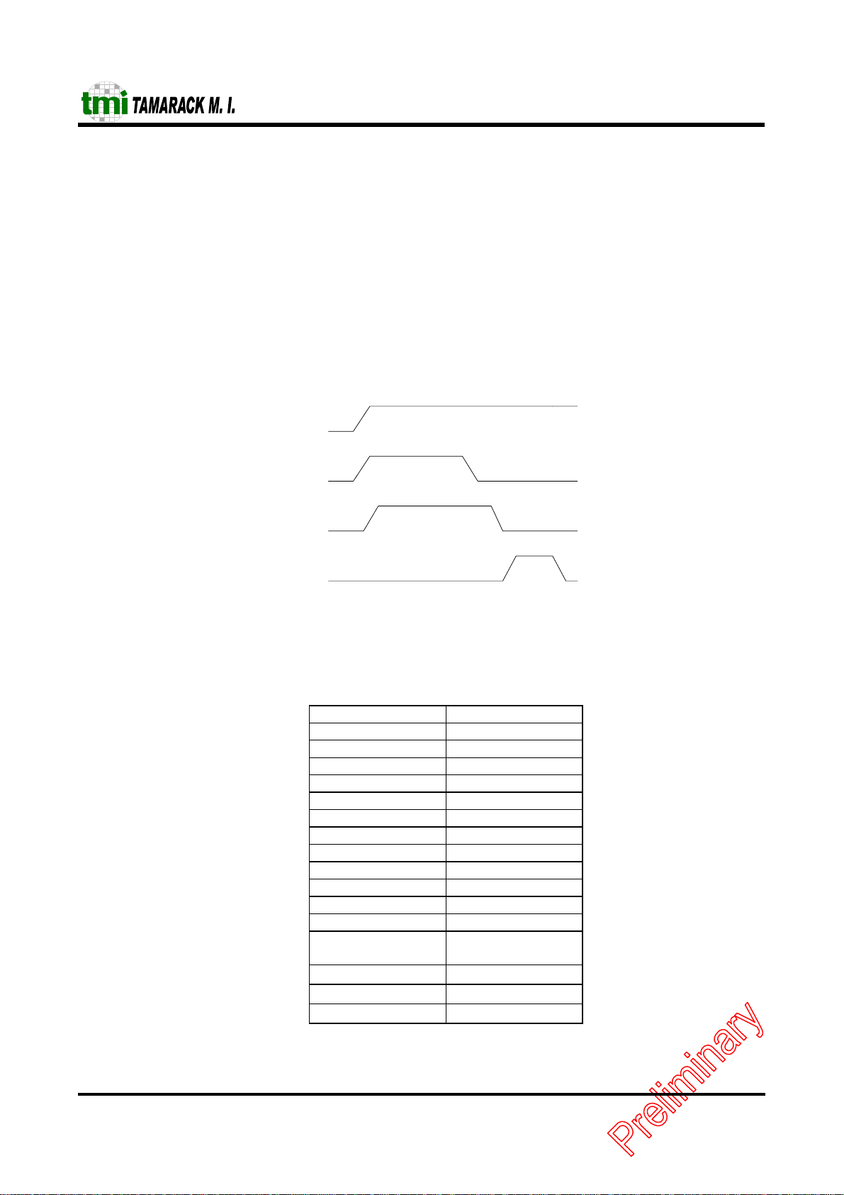
3.3 Power On Configurat ion
The TC5299J Controller configures itself after a RST signal is applied. When a Power-On-Reset occurs the
TC5299J controller latches up the values on the configuration pins and uses these to co n figure the internal registers
and options. Internally these pins contain pull-up resistance. If pins are unconnected they have default logic. The
configuration registers are loaded JMP0 & JMP1 setting when RST goes inactive.
A Power-On-Reset also causes the Controller to load the internal PROM from the EEPROM, which can take up to
3 ms. This occurs after “Config-Regs.” has completed. If EECONFIG is hi gh the configuration data loaded on the
falling edge of RST will be overwritten with data read from the serial EEPROM. Regardless of the level on
EECONFIG the PROM store will always be loaded with data from the serial EEPROM during the time specified
as EELOAD.
Figure 1 shows how the RESET circuitry operates.
VCC
RESET
TC5299J
Regload
EEload
The TC5299J Controller use a 93C56/66 EEPROM, The programmed contents of the EEPROM is shown as
following.
D15 D8 D7 D0
CIS byte n CIS byte n-1
13H ........ ........
12H ........ ........
11H CIS byte 3 CIS byte 2
10H CIS byte 1 CIS byte 0
0FH Not Used Config C
0EH Config. B Config. A
::::: Reserved Reserved
08H 42H 42H
07H 57H 57H
::::: Reserved Reserved
04H Reserved Reserved
03H Reserved bit [0]: 8-bit enable
bit [7:1]: Reserved
02H
01H
00H
Enet Address 5 Enet Address 4
Enet Address 3 Enet Address 2
Enet Address 1 Enet Address 0
EEPROM Programming Map
-8-
Ver. 0.1
07/04/01

Storing and Loading Configuration from EEPROM:
During boot up the TC5299J Controller's configuration is read from the EEPROM, before the PROM data is read. The
configuration data is stored within the address 0EH, 0FH (as above table) of the EEPROM's address space.
Configuration Register A, B and C are located in the address 0EH.
To write this configuration into the EEPROM, the user can program register in TC5299J's address 02H of page 3. This
operation will work regardless of the level on EECONFIG.
TC5299J
-9-
Ver. 0.1
07/04/01
TC5299J
4 I/O and Mapping
4.1 I/O Port Address M apping
This chip is register-liked with Novell's NE2000. The base I/O address of TC5299J Controller is configured by
Configuration Register (either upon po wer up or by software writing to this register). At that address the following
structure appears.
Base+00H
Base+0FH
Base+10H
Base+17H
Base+18H
Base+1FH
The registers within this area are 8 bits wide, but the data transfer port is 16 bits wide. By accessing the data transfer
port (using I/O instructions) the user can transfer data to or from the TC5299J 's internal memory.
4.2 EEPROM/SRAM Memory Mapping
The TC5299J Controller's internal memory map is as shown below.
D15 D7 D0
0000H
001FH
4000H
7FFFH
TC5299J Core Memory Map
PROM
Location
00h ETHERNET ADDRESS 0
01h ETHERNET ADDRESS 1
02h ETHERNET ADDRESS 2
03h ETHERNET ADDRESS 3
04h ETHERNET ADDRESS 4
05h ETHERNET ADDRESS 5
06-0Dh RESERVED
0E,0Fh 57h
10-15h ETHERNET ADDRESS 0-5
16-1Dh RESERVED
1E-1Fh 42h
Contents of PROM Map
Data Transfer Port
Location Contents
TC5299J
Core
Registers
Reset Port
PROM
Reserved
8K x 16
Buffer RAM
-10-
Ver. 0.1
07/04/01
 Loading...