

TL Electronic SlimLine PT 1082 Series, SlimLine PT 15-1082 Series, SlimLine PT 17-1082 Series, SlimLine PT 19-1082 Series Service Manual

ÐÐ2DQUHBD Manual for
IndustrialÐ/@MDK PC
2lHLLine /3Ðxxa
,QWHOUG*HQ&RUH¥LLL&38
µµµ+LJK3HUIRUPDQFH
)DQOHVV3DQHO3&
:LWK9*$',2/$1
TL Electronic GmbH
Bgm.-Gradl-Str. 1
85232 Bergkirchen-Feldgeding
Tel.: +49 (0)8131 33204-0
Fax: +49 (0)8131 33204-150
E-Mail: info@tl-electronic.de
www.tl-electronic.de
Germany
M1

!
Intel® Core™ 3rd Gen. Mobile
i3/i5/i7 High Performance
15”/17”/19” Fanless Embedded PC
COPYRIGHT NOTICE & TRADEMARK
All trademarks and registered trademarks mentioned herein are the property of their
respective owners.
This manual is copyrighted in Sep. 2013. You may not reproduce or transmit in any
form or by any means, electronic, or mechanical, including photocopying and
recording.
DISCLAIMER
This user’s manual is meant to assist you in installing and setting up the system. The
information contained in this document is subject to change without any notice.
CE NOTICE
This is a class A product. In a domestic environment this product may cause radio
interference in which case the user may be required to take adequate measures.
!

FCC NOTICE
This equipment has been tested and found to comply with the limits for a Class A
digital device, pursuant to part 15 of the FCC Rules. These limits are designed to
provide reasonable protection against harmful interference when the equipment is
operated in a commercial environment. This equipment generates, uses, and can
radiate radio frequency energy and, if not installed and used in accordance with the
instruction manual, may cause harmful interference to radio communications.
Operation of this equipment in a residential area is likely to cause harmful interference
in which case the user will be required to correct the interference at his own expense.
You are cautioned that any change or modifications to the equipment not expressly
approve by the party responsible for compliance could void your authority to operate
such equipment.
CAUTION! Danger of explosion if battery is incorrectly replaced. Replace only with the same or
equivalent type recommended by the manufacturer. Dispose of used batteries according to the
manufacturer’s instructions.
WARNING! Some internal parts of the system may have high electrical voltage. And therefore
we strongly recommend that qualified engineers can open and disassemble the system. The
LCD and touch screen are easily breakable, please handle them with extra care.
!

Contents
TABLE OF CONTENTS
CHAPTER 1 INTRODUCTION
1-1 About This Manual.................................................................... 1-2
1-2 System Illustration...................................................................... 1-3
1-3 System Specifications................................................................. 1-9
1-4 Safety Precautions...................................................................... 1-11
CHAPTER 2 SYSTEM CONFIGURATION
2-1 Jumper & Connector Quick Reference Table............................. 2-2
2-2 Component Locations................................................................ 2-3
2-3 How to Set Jumpers................................................................... 2-5
2-4 Clear CMOS Data Selection…………………………………... 2-7
2-5 CFast Voltage Selection............................................................. 2-7
2-6 COMPorts & Connectors….......................……..……………... 2-8
2-7 COM Ports RI & Voltage Selection…..........…..…………....... 2-9
2-8 COM2 RS232/422/485 Selection............................................... 2-10
2-9 COM2 Auto Detect Selection.................................................... 2-11
2-10 DIO Connector…….............……………………...................... 2-11
2-11 Flash Descriptor Override Selection…………………………... 2-12
2-12 Front Panel Connector & Selection…………………………… 2-13
2-13 Internal Keyboard & Mouse Connectors.................................... 2-14
2-14 Hardware Power Failure Selection.…………………………… 2-14
2-15 JUSB Port Connector………………………………………….. 2-15
2-16 LAN Connector………………………………………………... 2-15
2-17 Printer Port…………………………………………………….. 2-16
2-18 LVDS Connector……………………………………................ 2-17
2-19 LVDS Inverter Connector……………………………………... 2-17
2-20 LVDS Panel Brightness Control Selection……………………. 2-18
2-21 LVDS Voltage Selection………………………………………. 2-18
2-22 Power Input Connector………………………………………... 2-19
2-23 SATA & SATA Power Connectors…………………………… 2-20
!

Contents
2-24 Audio Connector………………………………………………. 2-21
2-25 System Fan Connector ………………………………............ 2-22
2-26 USB 3.0 Connector……………………………………………. 2-22
2-27 VGA Connector……………………………………………….. 2-23
2-28 SIM Card Slot…………………………………………………. 2-23
CHAPTER 3 SOFTWARE UTILITIES
3-1 Introduction................................................................................ 3-2
3-2 Intel
3-3 Intel
3-4 Intel
®
Chipset Software Installation Utility…..…….................. 3-3
®
USB3.0 eXtensible Host Controller Utility...................... 3-4
®
Management Engine Components Utility........................ 3-5
3-5 VGA Driver Utility.................................................................... 3-6
3-6 LAN Driver Utility…………………………………………….. 3-7
3-7 Sound Driver Utility…………………………………………… 3-8
3-8 Touchscreen Driver Utility……………………………………. 3-9
CHAPTER 4 AMI BIOS SETUP
4-1 Introduction................................................................................ 4-2
4-2 Entering Setup............................................................................ 4-4
4-3 Main……................................................................................... 4-6
4-4 Advanced…………………….........................…....................... 4-7
4-5 Chipset…………….................................................................... 4-27
4-6 Boot..……………….................................................................. 4-35
4-7 Security………………………………………………………... 4-36
4-8 Save & Exit……………………………………………………. 4-37
APPENDIX A SYSTEM DIAGRAMS
Exploded Diagram for Basic Construction............................................ A-2
Exploded Diagram for Front Panel………............................................ A-3
Exploded Diagram for Mainboard…………………............................. A-9
Exploded Diagram for Heatsink Cover………...................................... A-11
Exploded Diagram for HDD…………...………................................... A-13
!

Contents
APPENDIX B TECHNICAL SUMMARY
Block Diagram...................................................................................... B-2
Interrupt Map......................................................................................... B-3
DMA Channels Map……...................................................................... B-8
I/O Map................................................................................................. B-9
Watchdog Timer Configuration…………..…………………………... B-13
Flash BIOS Update……………………………………………………. B-15
!
!

INTRODUCTION!
This chapter gives you the information for this system. It
also outlines the System specification.
Section includes:
z About This Manual
z System Specifications
z Safety Precautions
!
!!
CHAPTER
1
!
Experienced users can skip to chapter 2 on page 2-1
for Quick Start.
Page:1-1

Chapter 1 Introduction
1-1. ABOUT THIS MANUAL
Chapter 1 Introduction
This chapter introduces you to the background of this manual, and the specifications
for this system. The final page of this chapter will indicate how to avoid damaging this
board.
Chapter 2 Hardware Configuration
This chapter outlines the component locations and their functions. In the end of this
chapter, you will learn how to set jumper and how to configure this card to meet your
own needs.
Chapter 3 Software Utilities
This chapter contains helpful information for proper installations of the VGA utility,
LAN utility, and Sound utility.
Chapter 4 BIOS Setup
This chapter indicates you how to set up the BIOS configurations.
Appendix A System Diagrams
This appendix gives you the exploded diagrams and part numbers of the system.
Appendix B Technical Summary
This appendix gives you the information about the Technical maps, Watchdog-timer
configuration, and Flash BIOS Update.
Page: 1-2
Chapter 1 Introduction
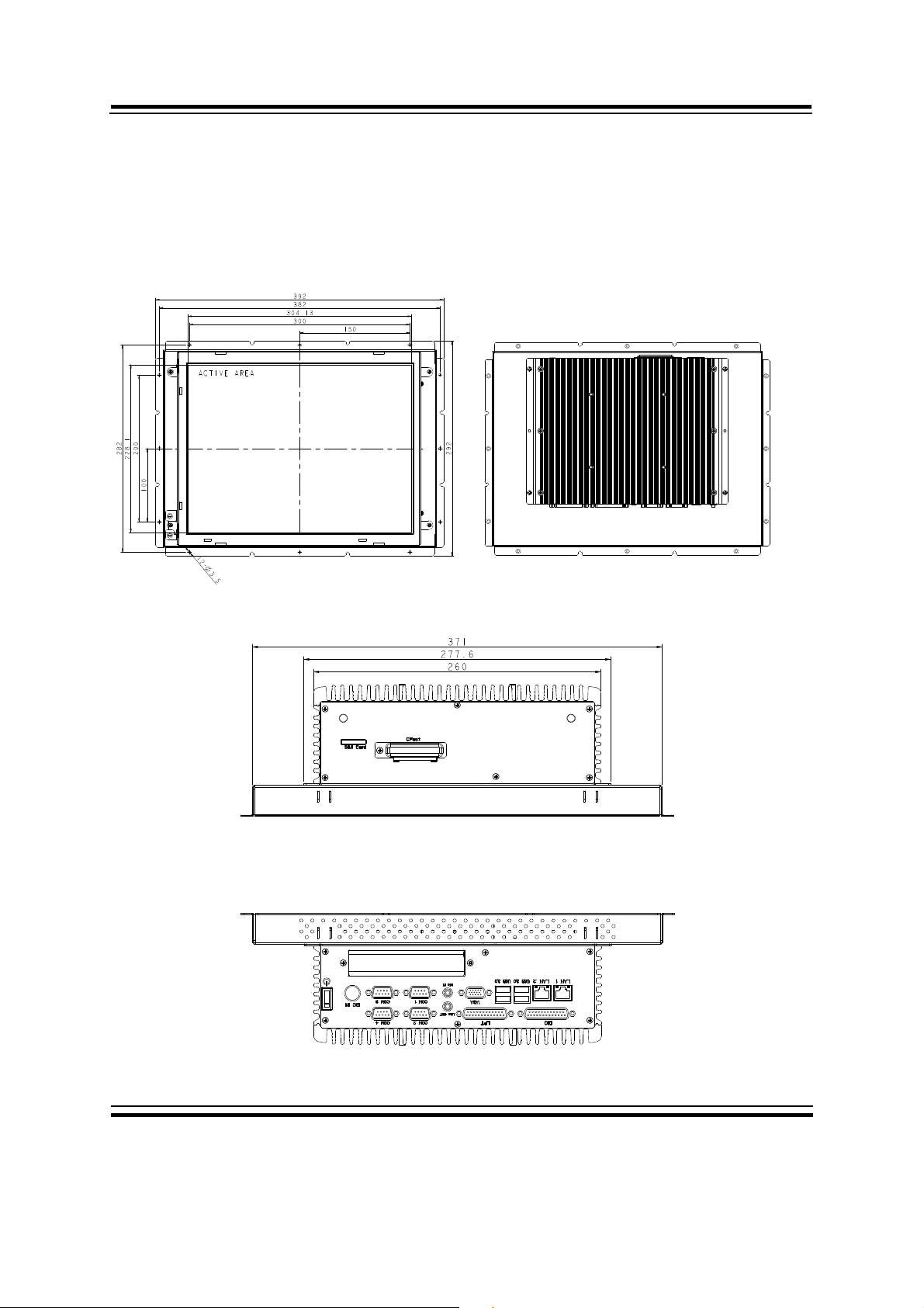
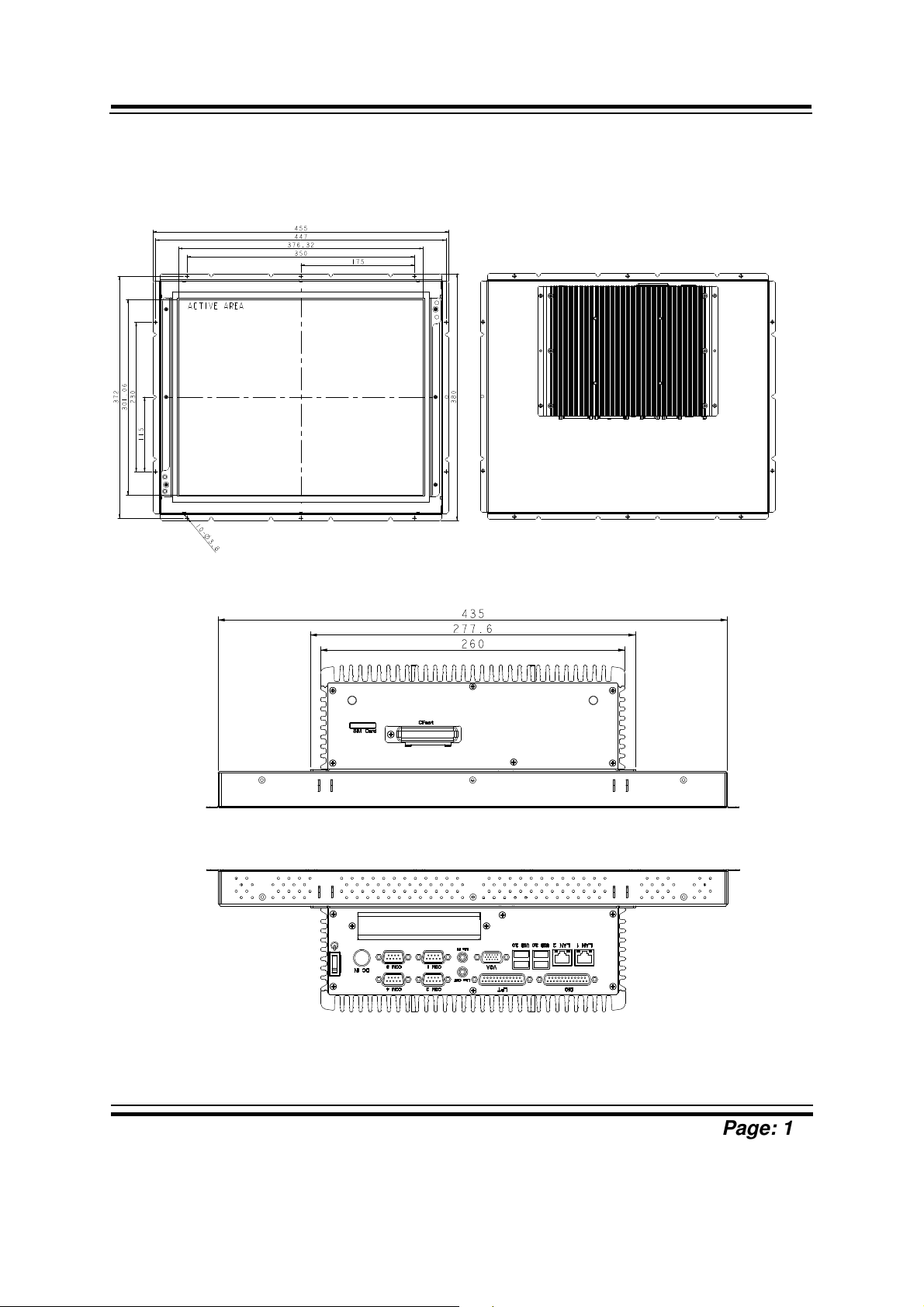
1-2. SYSTEM ILLUSTRATION
2KHL+HMDÐ/3Ða
Front View Rear View
Top View
Bottom View
Unit: mm
Page: 1-3
Side View Quarter View
Chapter 1 Introduction
Unit: mm
Page: 1-4
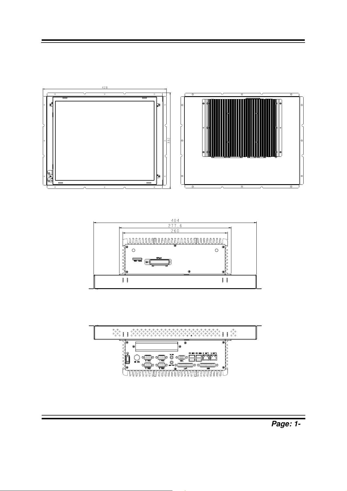
2KHL+HMDÐ/3Ða
Front View Rear View
Chapter 1 Introduction
T
op View
Bottom V
iew
Unit: mm
!!!!
!!!!
Page: 1-5
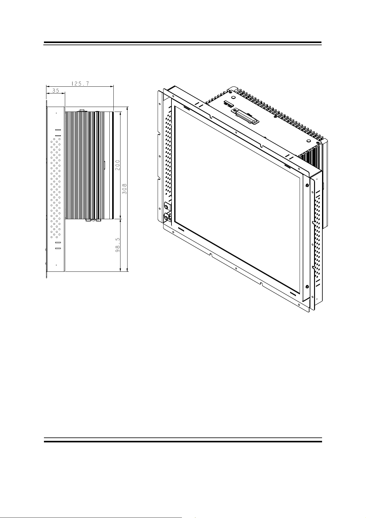
Side View Quarter View
Chapter 1 Introduction
Unit: mm
Page: 1-6
2KHL+HMDÐ/3Ða
Front View Rear View
Chapter 1 Introduction
Top View
Bottom View
Unit: mm
!!!!
!!!!
Page: 1-7
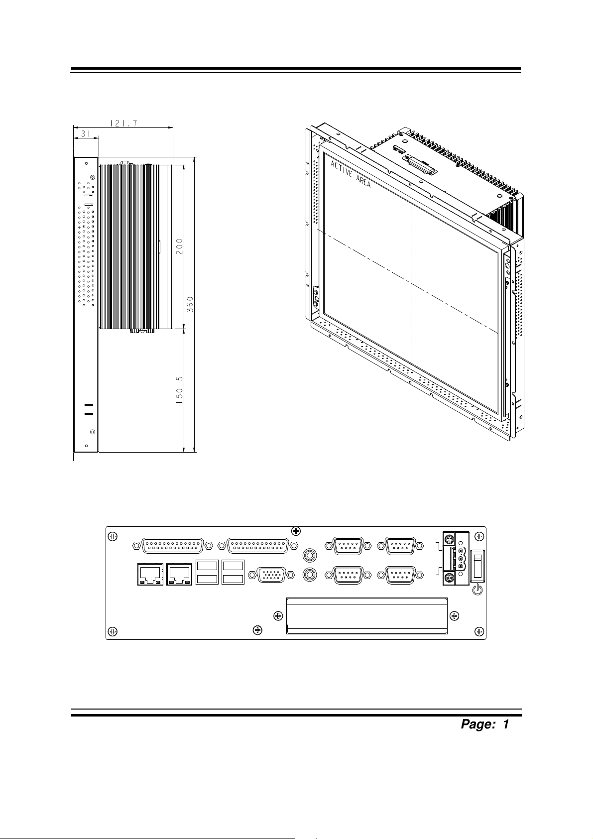
Chapter 1 Introduction
Side View Quarter View
I/O View
DIO LPT
LAN1 LAN2
USB3.0
VGA
Line
Out
Mic In
COM2 COM4
COM1 COM3
9-36V
DC
GND
Unit: mm
!!!!
!!!!
Page: 1-8

1-3. SYSTEM SPECIFICATION
System
CPU Support Intel
Chipset Intel® HM76/QM77
OS Support Microsoft Windows XP/7
®
Core™ 3rd Gen. Mobile i3/i5/i7 (rPGA-988)
processor on board
Chapter 1 Introduction
Memory Support
2 x 204pin DDR3 SO-DIMM, support DDR3/DDR3L
1600/1333/1066 up to 8GB/slot
Watchdog
1~255s Watchdog timer
Drive Bay 2 x 2.5” SATA HDD
Power Supply DC-in 9~36V
Front Bezel Aluminum
IP65 Front panel only
Mounting Type
Net Weight
Dimension
PT 15
PT 15
PT 17
PT 17
PT 19
PT 19
PT 15
PT 17
PT 19
VESA 100/Wall Mount
7.5 kg
9 kg
11.5 kg
408 x 308 x 128 mm
448 x 352 x 136 mm
471 x 396 x 131 mm
Certificate FCC/CE
I/O Ports
Serial Port
4 x COM ports (pin-9 is RI/5V/12V selectable):
COM1/3/4 for RS-232
COM2 for RS-232/422/485
USB 4 x USB 3.0
Parallel Port 1 x DSUB-25
VGA 1 x VGA
LAN 2 x LAN (10/100/1000 Mbps), support Wake-on-LAN:
LAN1: Intel
LAN2: Intel
!!!!
!!!!
®
82579LM
®
82583V
Page: 1-9
Chapter 1 Introduction
Audio High Definition:
1 x Line-out
1 x MIC-in
Digital I/O 1 x DSUB-25 (8in/8out)
Expansion slot 1 x Mini-PCIe slot (for WLAN module & 3G module)
1 x SIM card slot
1 x CFast card slot
1 x PCIe(4x), 10W/slot max. (Optional)
Display
LCD Panel Size
Resolution
PT 15
PT 17
PT 19
PT 15
PT 17
PT 19
15”
17”
19”
1024 x 768 XGA 400nit LED backlight
1280 x 1024 SXGA 350nit LED backlight
1280 x 1024 SXGA 300nit LED backlight
Touchscreen ( 5W Analog resistive (USB interface)
Environment
Operation Temp.
(with ambient airflow)
General: 0 ~ 45°C
CFast card (Wide Temp. Grade, w/o
audio): 0 ~ 50°C
Storage Temp. -20 ~ 80°C
Humidity 10 ~ 90%
!!!!
!!!!
Page: 1-10

Chapter 1 Introduction
1-4. SAFETY PRECAUTIONS
Follow the messages below to avoid your systems from damage:
1. Keep your system away from static electricity on all occasions.
2. Prevent electric shock. Don’t touch any components of this card when the card is
power-on. Always disconnect power when the system is not in use.
3. Disconnect power when you change any hardware devices. For instance, when
you connect a jumper or install any cards, a surge of power may damage the
electronic components or the whole system.
!
!!!!
!!!!
Page: 1-11

HARDWARE
CHAPTER
2
CONFIGURATION
** QUICK START **
Helpful information describes the jumper & connector settings, and
component locations.
Section includes:
z Jumper & Connector Quick Reference Table
z Component Locations
z Configuration and Jumper settings
z Connector’s Pin Assignments
Page 2-1

Chapter 2 Hardware Configuration
2-1. JUMPER & CONNECTOR QUICK REFERENCE TABLE
JUMPER/CONNECTOR NAME
Clear CMOS Data Selection JP5
CFAST Voltage Selection JP8
COM Ports COM1, COM2, COM3, COM4
COM Ports RI & Voltage Selection JP15, JP16, JP17, JP18
COM2 RS232/422/485 Selection JP13
COM2 Auto Detect Selection JP12
Digital I/O Connector DIO1
Flash Descriptor Override Selection JP3
Front Panel Selection PWRBTN1, HDDLED1, SYSRST1,
PWRLED1
Internal Keyboard & Mouse Connectors KB1, MS1
Hardware Power Failure Selection JP7
JUSB Connector JUSB1
LAN Connectors LAN1, LAN2
Printer Connector LPT1
LVDS Connector LVDS1
LVDS Inverter Connector INV1
LVDS Panel Brightness Control JP21
LVDS Voltage Selection JP19
Power Input Connector PWR_IN1, ATX_PWR1
SATA & SATA Power Connectors SATA1, SATA_PWR1, SATA2,
SATA_PWR2
Audio Connectors AUDIO1, LINE_IN1
System Fan Connector SYS_FAN1
USB3.0 Connectors USB1, USB2
VGA Connector VGA1
SIM Card Slot SIM1
Page: 2-2
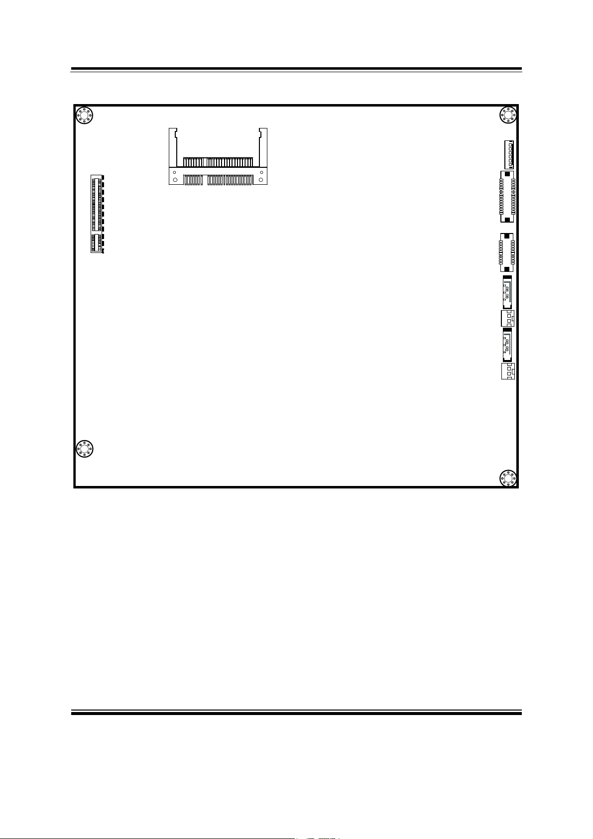
2-2. COMPONENT LOCATIONS
5
1
JP20
JP19
56
12
JP61JP5
1
SP1
12
JP10
87
1
KB1
1
MS1
JP21
Battery
1
234
2
1
DIO1
SO_DIMM2
20
19
JP3
1
1
JP4
210
19
USB5
®
Intel
HM76/
QM77
1
1
2
2
71
72
71
72
73
74
73
74
Intel® Core™
3rd Gen.
Mobile i3/i5/i7
(rPGA-988)
Chapter 2 Hardware Configuration
SIM1
14
1
M_PCIE1
LPT1
26
13
PWRBTN1
SIO
1
JP7
JP8
1
9
2
10
1
SYSRST1
1
PWRLED1
1
HDDLED1
11
JP9
1
1
12
1211
1
IR1
JP14
JP22
SYS_FAN1
203
204
B9
B1
A9
A1
LAN2LAN1
USB1
B1
A9
A1
USB2
SO_DIMM1
203
204
9
10
JP13
LINE_IN1
5
10
15
VGA1
1
JP12
1
6
11
1
2
1
AUDIO1
21 24
15
125
JP17
10
15
1
4
6
125
JP18
6
6
14
18
5
9
COM1/2
Connectors, Jumpers and Components Locations
JP15 JP16
1256125
10
18
15
1
9
6
COM3/4
6
14
5
ATX_PWR1
2
4
3
1
4
3
2
1
PWR_IN1
Page: 2-3
Chapter 2 Hardware Configuration
3&,B(
JCFAST1
S1S7PC1 PC17
INV1
LVDS1
JUSB1
SATA1
SATA_PWR1
SATA2
SATA_PWR2
6
1
1292
30
1192
20
7
1
1
7
1
1
Connectors, Jumpers and Components Locations
Page: 2-4
Chapter 2 Hardware Configuration
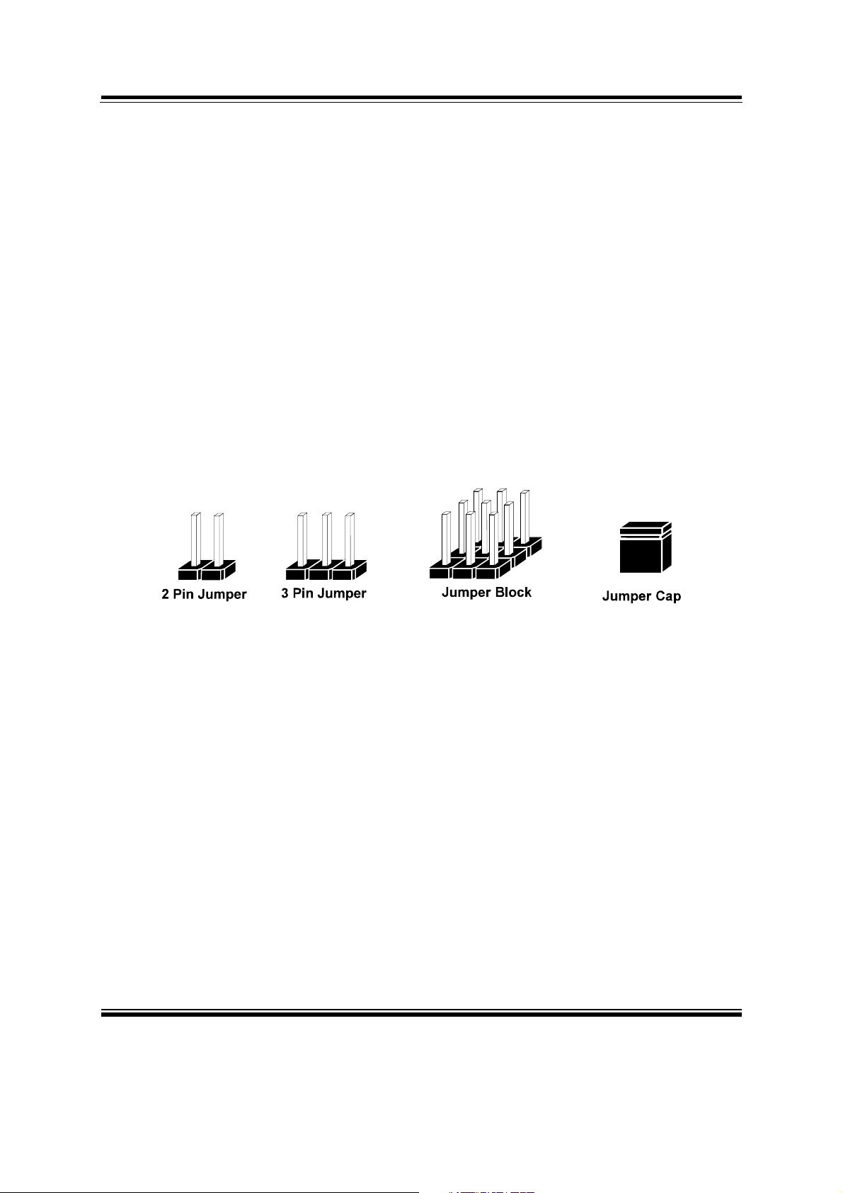
2-3. HOW TO SET JUMPERS
You can configure your board by setting jumpers. Jumper is consists of two or three
metal pins with a plastic base mounted on the card, and by using a small plastic "cap",
Also known as the jumper cap (with a metal contact inside), you are able to connect
the pins. So you can set-up your hardware configuration by "open" or "close" pins.
The jumper can be combined into sets that called jumper blocks. When the jumpers
are all in the block, you have to put them together to set up the hardware configuration.
The figure below shows how this looks like.
JUMPERS AND CAPS
If a jumper has three pins (for examples, labelled PIN1, PIN2, and PIN3), You can
connect PIN1 & PIN2 to create one setting by shorting. You can either connect PIN2
& PIN3 to create another setting. The same jumper diagrams are applied all through
this manual. The figure below shows what the manual diagrams look and what they
represent.
Page: 2-5
JUMPER DIAGRAMS
Chapter 2 Hardware Configuration
Jumper Cap
looks like this
2 pin Jumper
looks like this
3 pin Jumper
looks like this
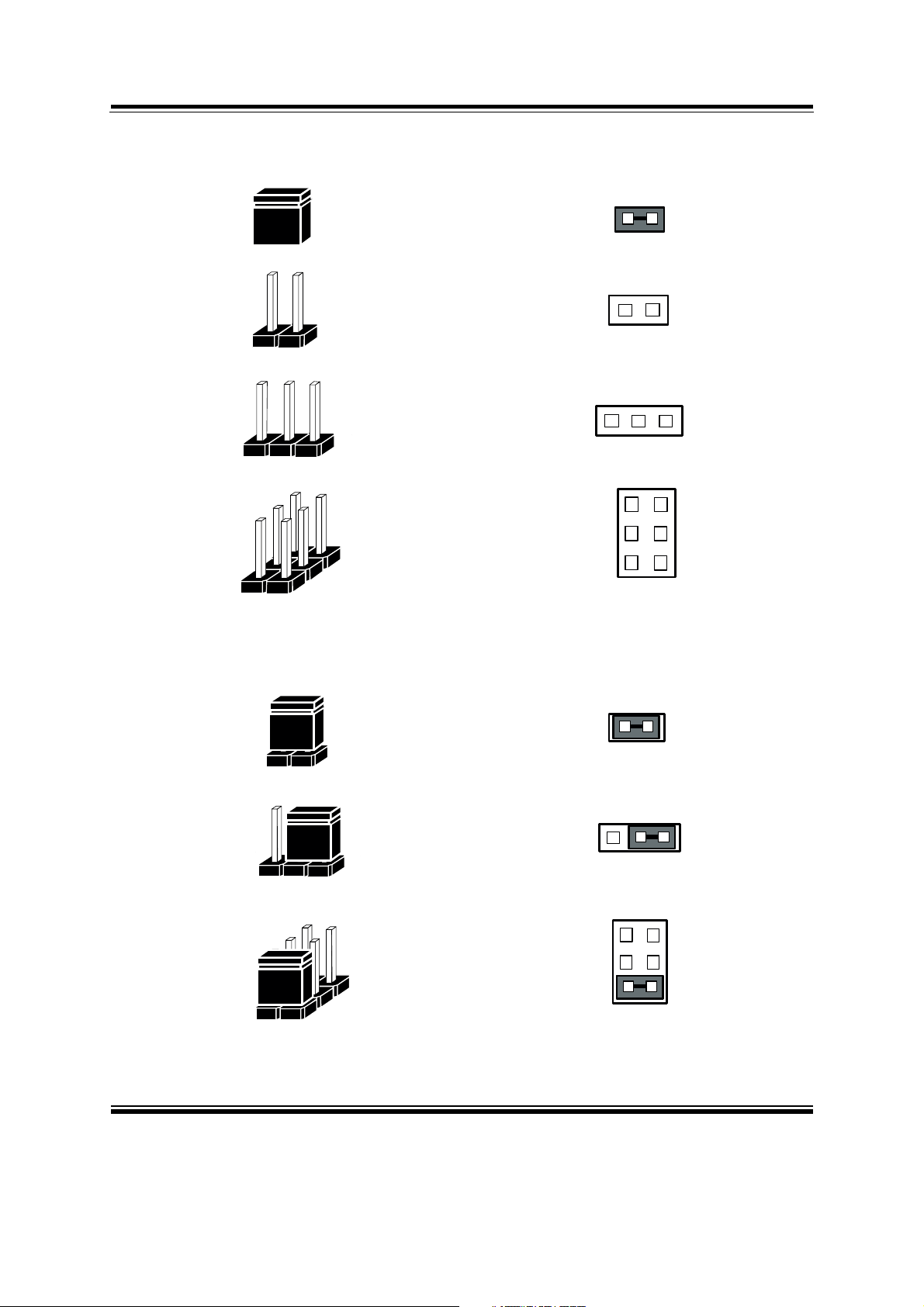
JUMPER SETTINGS
1
1
1
2
Jumper Block
looks like this
2 pin Jumper close(enabled)
Looks like this
3 pin Jumper
2-3 pin close(enabled)
Looks like this
Jumper Block
1-2 pin close(enabled)
Looks like this
1
1
12
Page: 2-6
Chapter 2 Hardware Configuration
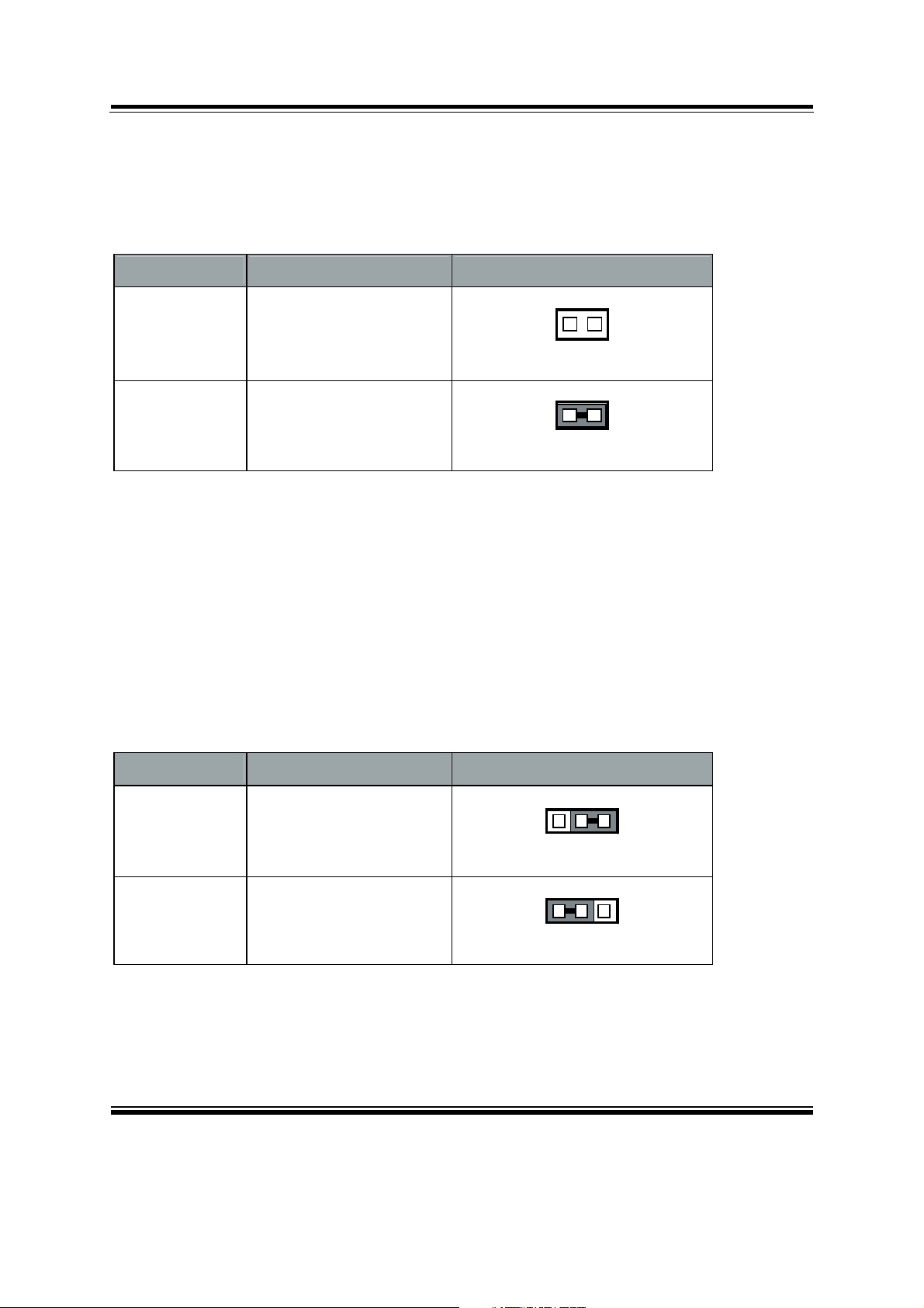
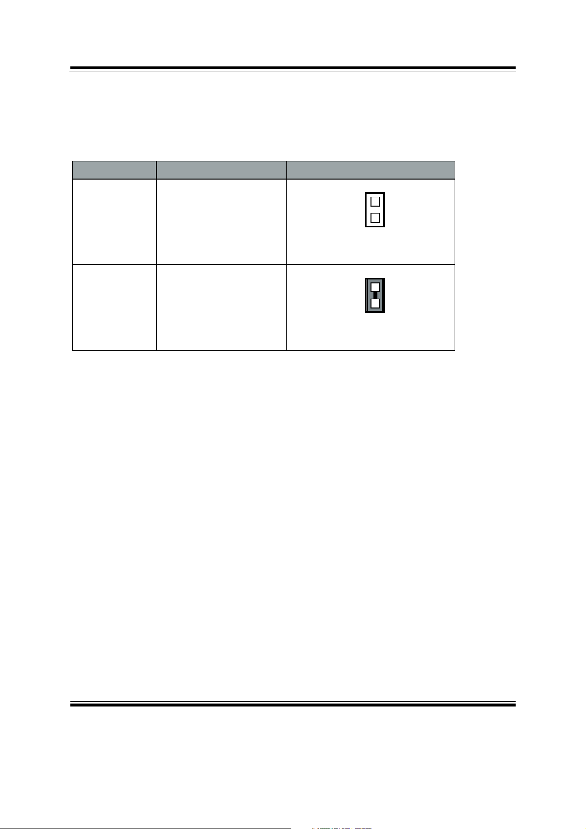
2-4. CLEAR CMOS DATA SELECTION
JP5 : Clear CMOS Data Selection
The jumper setting is as follows:
SELECTION JUMPER SETTINGS JUMPER ILLUSTRATION
1
Normal Open
-3
1
Clear CMOS* Close
-3
Note: Manufacturing Default is Normal.
*To clear CMOS data, user must power-off the computer and set the jumper to “Clear
CMOS” as illustrated above. After five to six seconds, set the jumper back to “Normal”
and power-on the computer.
2-5. CFAST VOLTAGE SELECTION
JP8 : CFast Voltage Selection
The jumper setting is as follows:
SELECTION JUMPER SETTINGS JUMPER ILLUSTRATION
3.3V 1-2
5V 2-3
Note: Manufacturing Default is 3.3V.
31
-3
31
-3
Page: 2-7

Chapter 2 Hardware Configuration
2-6. COM PORTS
COM1, COM3, COM4: COM Ports, fixed as RS-232
The pin assignments are as follows:
PIN ASSIGNMENT PIN ASSIGNMENT
1 DCD# 6 DSR#
2 RX 7 RTS#
3 TX 8 CTS#
4 DTR# 9 RI#
5 GND
COM2: COM2 Connector, selectable as RS-232/422/485
The pin assignments are as follows:
PIN
ASSIGNMENT
RS-232 RS-422 RS-485
1 DCD# TX- RS-4852 RX TX+ RS-485+
3 TX RX+ X
4 DTR# RX- X
5 GND GND GND
6 DSR# X X
7 RTS# X X
8 CTS# X X
9 RI# X X
1
6
&20
&20
&20
&20
5
9
Page: 2-8
Chapter 2 Hardware Configuration
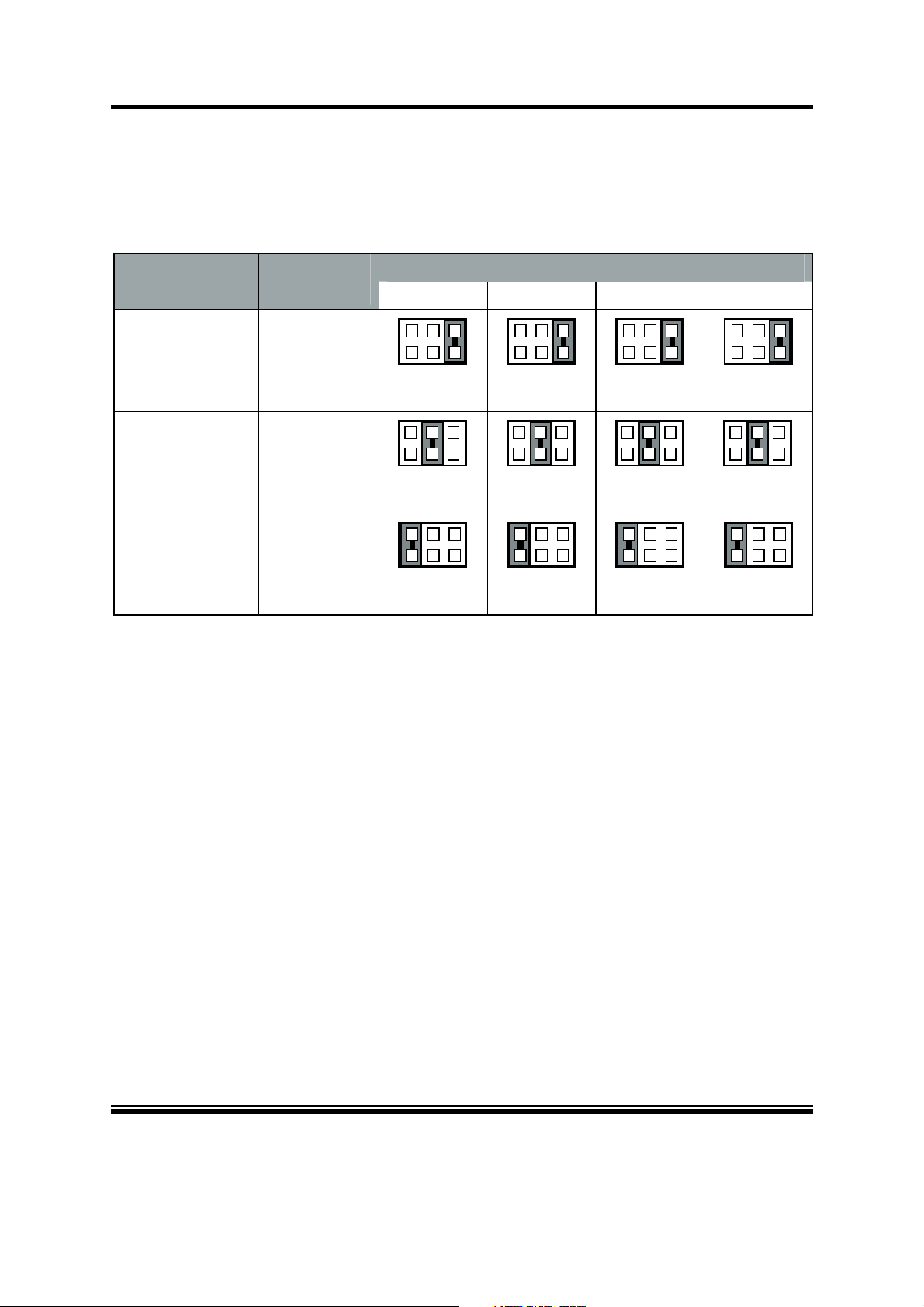
2-7. COM PORTS RI & VOLTAGE SELECTION
JP18, JP17, JP16, JP15: COM1/2/3/4 Ports RI & Voltage Selection
The selections are as follows:
JUMPER ILLUSTRATION SELECTION JUMPER
SETTING
COM1 COM2 COM3 COM4
RI 1-2
VCC12 3-4
VCC 5-6
Note: Manufacturing Default is RI.
5
6
-3
5
6
-3
5
6
-3
1
2
1
2
1
2
5
6
5
6
5
6
-3
-3
-3
1
2
1
2
1
2
5
6
5
6
5
6
-3
-3
-3
1
2
1
2
1
2
5
6
5
6
5
6
-3
-3
-3
1
2
1
2
1
2
Page: 2-9
Chapter 2 Hardware Configuration
2-8. COM2 RS-232/422/485 SELECTION
JP13: COM2 RS-232/422/485 Selection
The selections are as follows:
SELECTION JUMPER SETTINGS JUMPER ILLUSTRATION
1
2
RS-232 All open
9
10
-3
1
2
RS-422 1-2, 3-4, 9-10
9
10
-3
1
2
RS-485 1-2, 5-6, 7-8
9
10
Note: Manufacturing Default is RS-232.
-3
Page: 2-10
Chapter 2 Hardware Configuration
2-9. COM2 AUTO DETECT SELECTION
JP12: COM2 Auto Detect Selection
The selections are as follows:
SELECTION JUMPER SETTINGS JUMPER ILLUSTRATION
31
Normal 1-2
-3
31
Auto 2-3
-3
Note: Manufacturing Default is Auto.
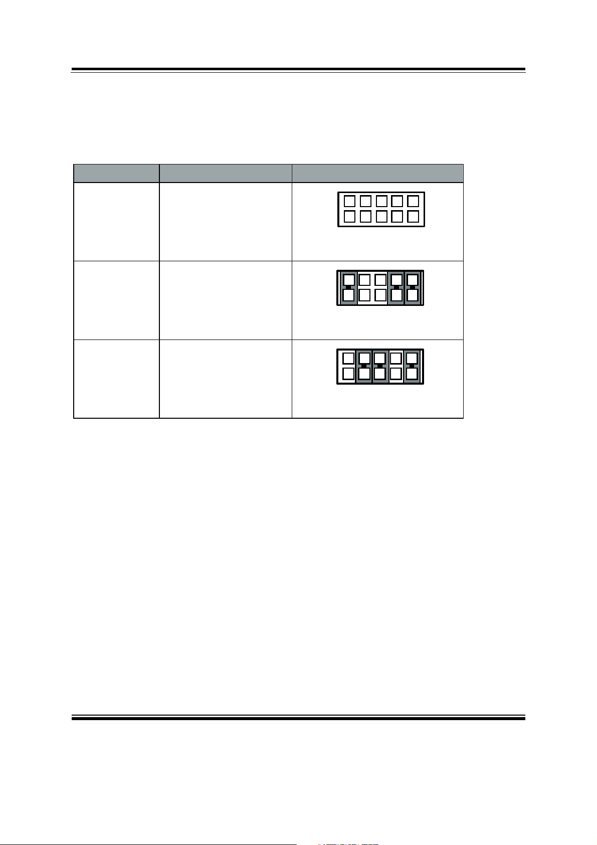
2-10. DIGITAL I/O CONNECTOR
DIO1: DIO Connector
The pin assignments are as follows:
PIN ASSIGNMENT PIN ASSIGNMENT
1 VCC5 11 DIN5
2 VCC12 12 DOUT5
3 DIN1 13 DIN6
4 DOUT1 14 DOUT6
5 DIN2 15 DIN7
6 DOUT2 16 DOUT7
7 DIN3 17 DIN8
8 DOUT3 18 DOUT8
9 DIN4 19 GND
10 DOUT4 20 GND
202
119
',2
Page: 2-11
Chapter 2 Hardware Configuration
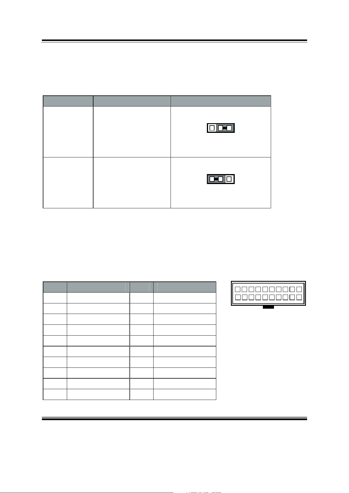
2-11. FLASH DESCRIPTOR OVERRIDE SELECTION
JP3: Flash Descriptor Override Selection
The selections are as follows:
SELECTION JUMPER SETTINGS JUMPER ILLUSTRATION
1
Disable Open
-3
1
Enable Close
-3
Note: Manufacturing Default is Disable.
Page: 2-12
Chapter 2 Hardware Configuration
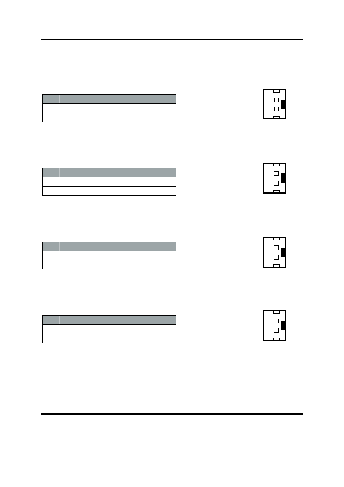
2-12. FRONT PANEL CONNECTORS
PWRBTN1: ATX Power Button Connector
The pin assignments are as follows:
PIN ASSIGNMENT
1
PWR_BTN
2 GND
HDDLED1: Hard Disk Drive LED Connector
The pin assignments are as follows:
PIN ASSIGNMENT
1
HDD_LED+
2 HDD_LED-
SYSRST1: Reset Connector
The pin assignments are as follows:
PIN ASSIGNMENT
1
2 GND
RST_BTN
1
2
3:5%71
1
2
+''/('
1
2
PWRLED1: Power LED Connector
The pin assignments are as follows:
PIN ASSIGNMENT
1
PWR_LED+
2 GND
6<6567
1
2
3:5/('
Page: 2-13
 Loading...