


86(5
86(5····6
86(586(5
0$18$/
0$18$/
0$18$/0$18$/
$+
6OLPDQG)DQOHVV,QWHO
((-
SURFHVVRU(PEHGGHG3&
TL Electronic GmbH
6
66
5DQRHNMÐ
Bgm.-Gradl-Str. 1
85232 Bergkirchen-Feldgeding
Germany
Tel.: +49 (0)8131 33204-0
Fax: +49 (0)8131 33204-150
E-Mail: info@tl-electronic.de
www.tl-electronic.de

Contents
GDD!OPUJDF
This equipment has been tested and found to comply with the limits for a Class A
digital device, pursuant to part 15 of the FCC Rules. These limits are designed to
provide reasonable protection against harmful interference when the equipment is
operated in a commercial environment. This equipment generates, uses, and can
radiate radio frequency energy and, if not installed and used in accordance with the
instruction manual, may cause harmful interference to radio communications.
Operation of this equipment in a residential area is likely to cause harmful interference
in which case the user will be required to correct the interference at his own expense.
You are cautioned that any change or modifications to the equipment not expressly
approve by the party responsible for compliance could void your authority to operate
such equipment.
!
WARNING! Some internal parts of the system may have high
electrical voltage. And therefore we strongly recommend that
qualified engineers can open and disassemble the system.
RESTRICTED ACCESS LOCATION: access can only be gained by
SERVICE PERSONS or by USERS who have been instructed about
the reasons for the restrictions applied to the location and about any
precautions that shall be taken; and access is through the use of a
TOOL or lock and key, or other means of security, and is controlled
by the authority responsible for the location

Contents
TABLE OF CONTENTS
CHAPTER 1 INTRODUCTION
1-1 About This Manual.................................................................... 1-2
1-2 System Illustration...................................................................... 1-3
1-3 System Specifications................................................................. 1-5
1-4 Safety Precautions...................................................................... 1-7
CHAPTER 2 SYSTEM CONFIGURATION
2-1 Jumper & Connector Quick Reference Table............................. 2-2
2-2 Component Locations................................................................ 2-3
2-3 How to Set the Jumpers.............................................................. 2-5
2-4 PWR In Connector……..………………………….................... 2-7
2-5 COM Port & Connector……..…………………………............ 2-7
2-6 COM Port RI & Voltage Selection............................................ 2-10
2-7 USB Port…………………..…………………………………... 2-10
2-8 LAN Port………........................................................................ 2-12
2-9 DVI Connector........................................................................... 2-14
2-10 Digital I/O Connector…...………………………………….. 2-16
2-11 Audio Connector…………..…………………………………... 2-17
2-12 SATA & SATA Power Connector............................................. 2-18
2-13 CFAST Card Slot...……………………………………………. 2-19
2-14 CFAST Card Power Selection
įįį
.………………………............
2-19
2-15 Clear CMOS Data Selection…...………………………............ 2-20
2-16 DVI-D Enable Selection…...……………………….................. 2-20
2-17 DVI-D HPD Enable Selection…...……………………............. 2-21
2-18 DDC Selection……………………………………………….... 2-21
CHAPTER 3 SOFTWARE UTILITIES
3-1 Introduction................................................................................ 3-2
3-2 Intel
®
Chipset Software Installation Utility…..…….................. 3-3
3-3 Intel ® Trusted Execution Engine Driver installation…………
3-4 Intel ® Kernel-Mode Driver Framework Driver Installation….
3-4
3-5
3-5 Intel® Mailbox Interface Device Driver………….…………... 3-6
3-6 For USB3.0 Driver installation………………………………... 3-7
3-7 VGA Driver Utility.................................................................... 3-8
3-8 LAN Driver Utility..................................................................... 3-9
3-9 Sound Driver Utility................................................................... 3-10

Contents
CHAPTER 4 SYSTEM INSTALLATION
4-1 Removing the bottom case......................................................... 4-2
4-2 HDD Installation........................................................................ 4-4
4-3 SO-DIMM Installation……....................................................... 4-8
4-4 Wireless LAN or 3G module Installation…………................... 4-12
4-5 CFast Card Installation……………........................................... 4-17
4-6 PoE Board Installation…………………………………….…... 4-21
CHAPTER 5 AMI BIOS SETUP
5-1 Introduction................................................................................ 5-2
5-2 Entering Setup............................................................................ 5-4
5-3 Main……................................................................................... 5-6
5-4 Advanced…………………….........................…....................... 5-8
5-5 Chipset…………….................................................................... 5-43
5-6 Security………………………………………………………... 5-53
5-7 Boot..……………….................................................................. 5-54
5-8 Save & Exit……………………………………………………. 5-58
APPENDIX A SYSTEM ASSEMBLY
Exploded Diagram for Bottom Case………..….................................... A-2
Exploded Diagram for HDD Support Board.….................................... A-3
Exploded Diagram for Front & Rear Case…….................................... A-5
Exploded Diagram for Motherboard……..……................................... A-6
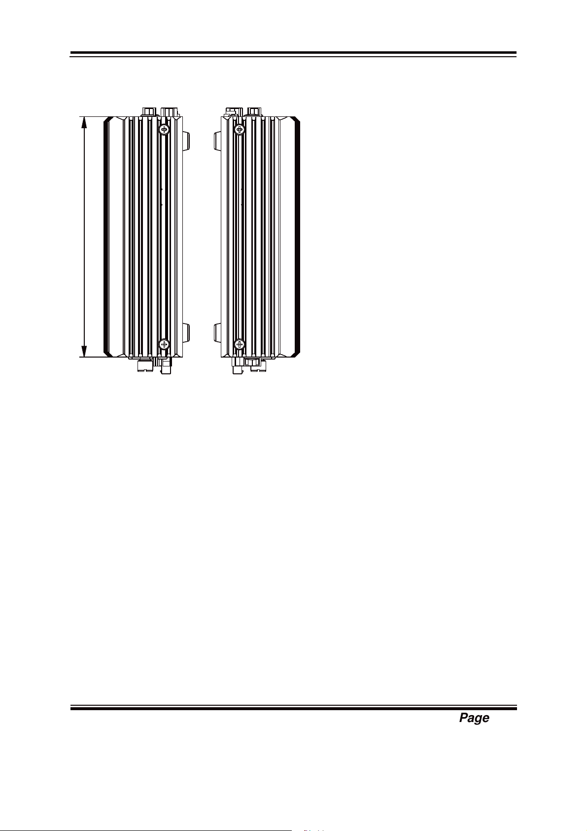
Exploded Diagram for Heatsink……………….................................... A-7
APPENDIX B TECHNICAL SUMMARY
Block Diagram...................................................................................... B-2
Interrupt Map......................................................................................... B-3
I/O Map................................................................................................. B-8
Memory Map………………………………………………………….. B-11
Watchdog Timer Configuration…………..…………………………... B-13
Flash BIOS Update……………………………………………………. B-15
!
!
!

!
!
!
!
!
!
!
INTRODUCTION!
!
!
!
This chapter gives you the information for EL1083. It also outlines
the System specification.
Section includes:
z About This Manual
z System Specifications
z Safety Precautions
!
!!
CHAPTER
1
!
Experienced users can skip to chapter 2 on page 2-1
for Quick Start.
!
Page:1-1

Chapter 1 Introduction
1-1. ABOUT THIS MANUAL
!
Thank you for purchasing our EL1083 Intel® E3845/E3826/J1900 Embedded PC.
EL1083 provides faster processing speed, greater expandability and can handle more
task than before. This manual is designed to assist you how to install and set up the
system. It contains four chapters. The user can apply this manual for configuration
according to the following chapters:
Chapter 1 Introduction
This chapter introduces you to the background of this manual, and the specifications
for this system. The final page of this chapter will indicate how to avoid damaging
this board.
Chapter 2 Hardware Configuration
This chapter outlines the component locations and their functions. In the end of this
chapter, you will learn how to set jumper and how to configure this card to meet your
own needs.
Chapter 3 Software Utilities
This chapter contains helpful information for proper installations of the VGA utility,
LAN utility, and Sound utility.
Chapter 4 AMI BIOS Setup
This chapter indicates you how to set up the BIOS configurations.
Appendix A System Assembly
This appendix gives you the exploded diagrams and part numbers of the (/.
Appendix B Technical Summary
This appendix gives you the information about the Block diagram, Technical maps,
Watchdog-timer configuration, and Flash BIOS Update.
!
!
Page: 1-2
Chapter 1 Introduction
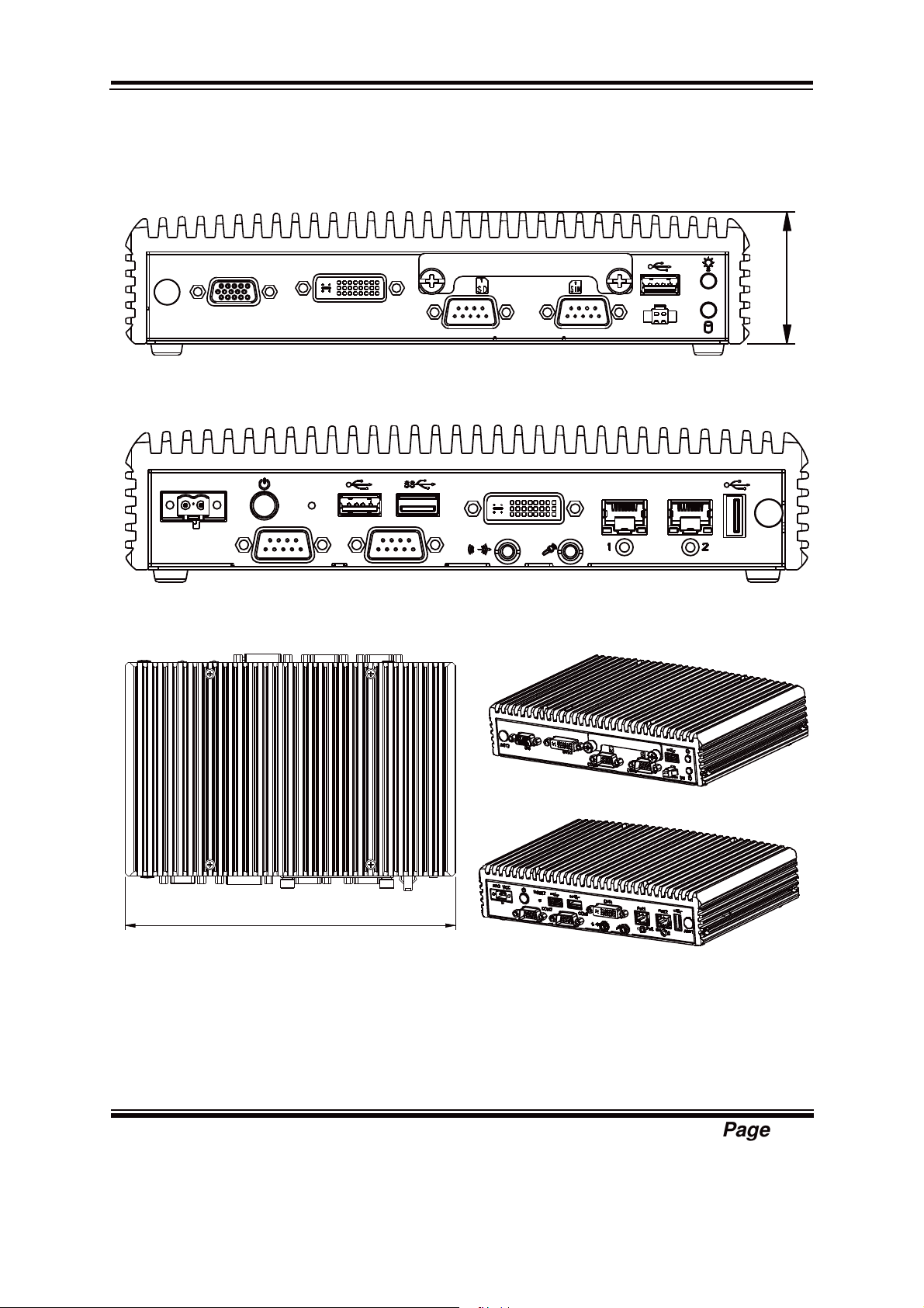
1-2. SYSTEM ILLUSTRATION
Front View
Reset
COM1
DVI-D
COM2
ANT2
Rear View
GND VCC
DIO
46
COM4COM3
DVI-I
Remote SW
LAN1
PoE
ON
LAN2
ANT1
Top View Quarter View
217.50
!
!
Page: 1-3
Chapter 1 Introduction
Side View
140.60
!
!
Page: 1-4

Chapter 1 Introduction
1-3. SYSTEM SPECIFICATION
System
CPU Support Intel® J1900/E3845/E3826 CPU
Chipset Intel® SOC
OS Support Win7/ Win8.1/ WES7/ WE 8.1 Industry Pro
Memory Support 1 x DDR3L SO-DIMM Socket (up to 8 GB)
Drive Bay 1 x 2.5 inch SATA HDD or SSD driver space
Power Requirement 9~36V DC-in
Watchdog 1~255s Watchdog timer
Expansion Slot
System Weight 2.5 kg
Dimension (W x H x D) 217.5 x 46 x 148 mm (8.56” x 1.77” x 5.83”)
Certificate FCC/CE
1x full size miniPCIe (PCIe+USB+external SIM card)
1x half size miniPCIe (PCIe+USB)
I/O Ports
Serial Port COM3/4 for RS232 (front), COM1/2 for +5v/+12v/RI
selectable by jumper,RS232/422/485 selectable by BIOS
Digital I/O 4-in/4-out (front)
USB 1 x USB 2.0 port (front), 2 x USB 2.0, 1 x USB 3.0 (rear)
DVI DVI 1 x DVI-D (front), 1 x DVI-I (rear)
SIM 1 x SIM card slot with cover
SD 1 x SD Card with cover
Audio Realtek high definition audio, 1x Line-Out & 1x MIC In
audio jack by pin header
LAN 2 x RJ45 connector with PoE support Wake on LAN/
PXE
Power ON/OFF 1x power button switch (rear), 1x 2pin connector for
remote power button (front)
Reset 1x reset (rear)
!
!
Page: 1-5

!
Environment
Chapter 1 Introduction
Operating Temp.
(with air)
0~45°C (32~113°F),with ST SSD
0~40°C (32~104°F), with HDD
-30~60°C (-22~140°F) with wide temp. peripherals w/o
PoE (w/o Audio) (E3845/E3826 only)
-30~55 °C (-22~131°F) with wide temp. peripherals with
PoE (w/o Audio) (E3845/E3826 only)
Storage Temp. -30 ~ 80°C (-22~ 176°F)
Humidity Operating: 10 ~ 90%, Storage: 10~95%RH
!
!
Page: 1-6

Chapter 1 Introduction
1-4. SAFETY PRECAUTIONS
Follow the messages below to avoid your systems from damage:
1. Keep your system away from static electricity on all occasions.
2. Prevent electric shock. Don’t touch any components of this card when the card is
power-on. Always disconnect power when the system is not in use.
3. Disconnect power when you change any hardware devices. For instance, when
you connect a jumper or install any cards, a surge of power may damage the
electronic components or the whole system.
!
!
!
Page: 1-7

HARDWARE
CHAPTER
2
CONFIGURATION
** QUICK START **
Helpful information describes the jumper & connector settings, and
component locations.
Section includes:
z Jumper & Connector Quick Reference Table
z Component Locations
z Configuration and Jumper settings
z Connector’s Pin Assignments
Page 2-1

Chapter 2 Hardware Configuration
2-1. JUMPER & CONNECTOR QUICK REFERENCE TABLE
JUMPER / CONNECTOR NAME
Pwr In Connector CN_POWER1
Com Port & Connector COM1, COM2, COM3, COM4, COM5,
COM6
Com Port Ri & Voltage Selection JPCOM1, JPCOM2
USB Port USB4, USB2, USB3, USB5
LAN Port LAN1, LAN2
DVI Connector DVI1, DVI2
Digital I/O Connector DIO1, JDIO1
Audio Connector JAUDIO1
SATA & SATA Power Connector SATA1, HDD_POWER1
CFast Card Slot CFAST1
CFast Card Power Connector JP11
Clear CMOS Data Selection JP1
DVI-D Enable Selection JP34, JP35
DVI-D HPD Enable Selection JP37
DDV Selection JP13
Page: 2-2
2-2. COMPONENT LOCATIONS
SW2
JP_COM1
JP36
6215
203
204
SW1
2
1
JPCOM1
COM1
USB4
JP17
21
DIMM1
COM2
JP18
21
USB5
JPCOM2
2
1
1
1
JP19
JP20
JP_COM2
1
2
JP13
CN_POWER1
12
Chapter 2 Hardware Configuration
LAN1 LAN2 USB2
DVI2
10
9
21
JAUDIO1
JP3
JDIO1
1
3
JP11
CFAST1
LED1
USB3
SLOT2
52
51
18
17
16
15
2
1
331
JP35
1
JP34
SLOT1
52
51
18
17
16
15
2
1
2
1
12
BAT1
12
1
7
JP1
SATA_PWR1
JP37
SATA1
12
DVI1
Connectors, Jumpers and Components Locations - Front
5
10
DIO1
JPOE1
S1 S7 PC1 PC17
JP9
JP10
COM3COM4COM5COM6
1
6
11 15
JLPC1
Page: 2-3
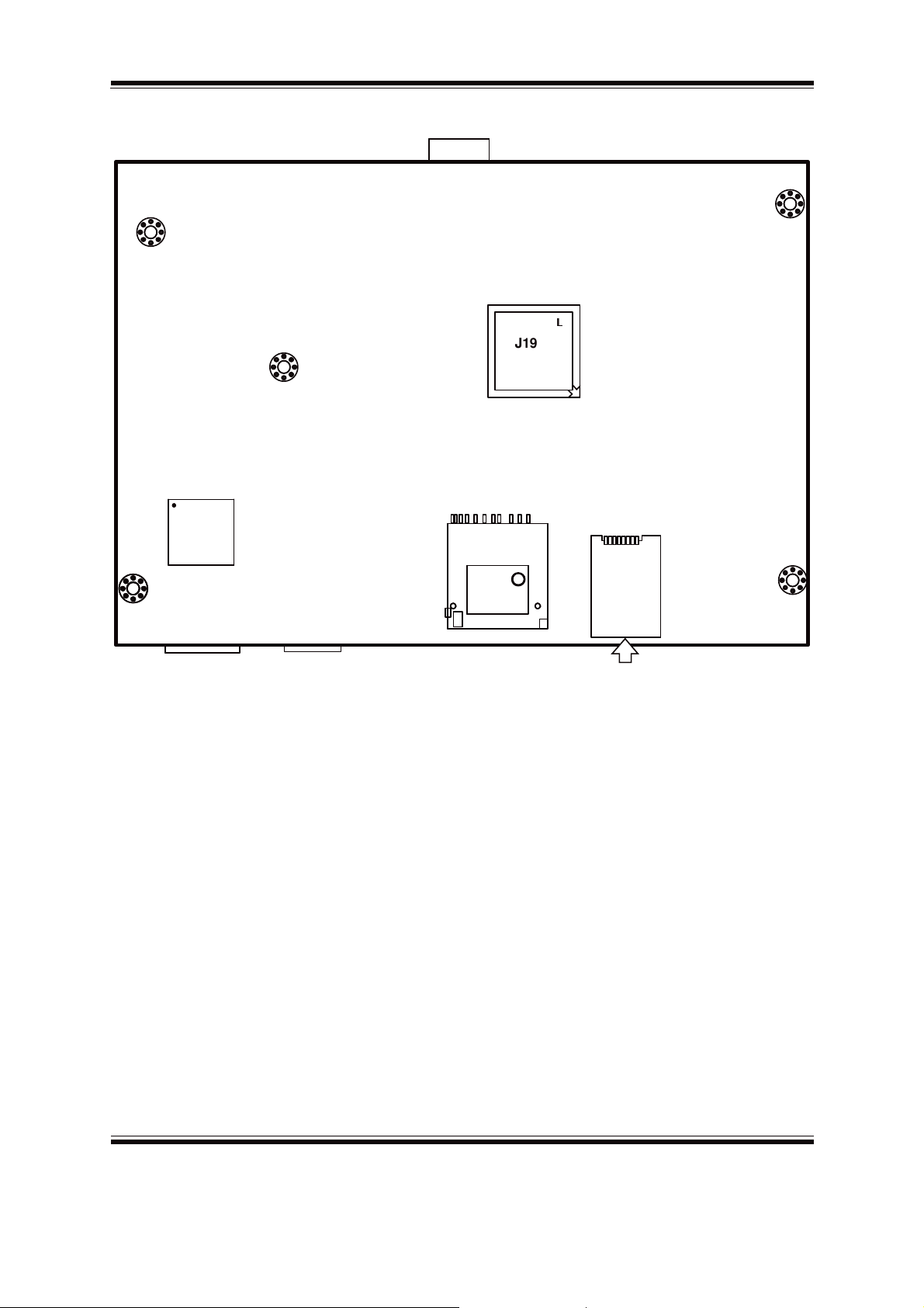
Chapter 2 Hardware Configuration
J1900/
E3845/
E3826
SD_CARD1
Intel
®
ٞٞٞٞ
SIO
Connectors, Jumpers and Components Locations - Rear
SIM1
Page: 2-4
Chapter 2 Hardware Configuration
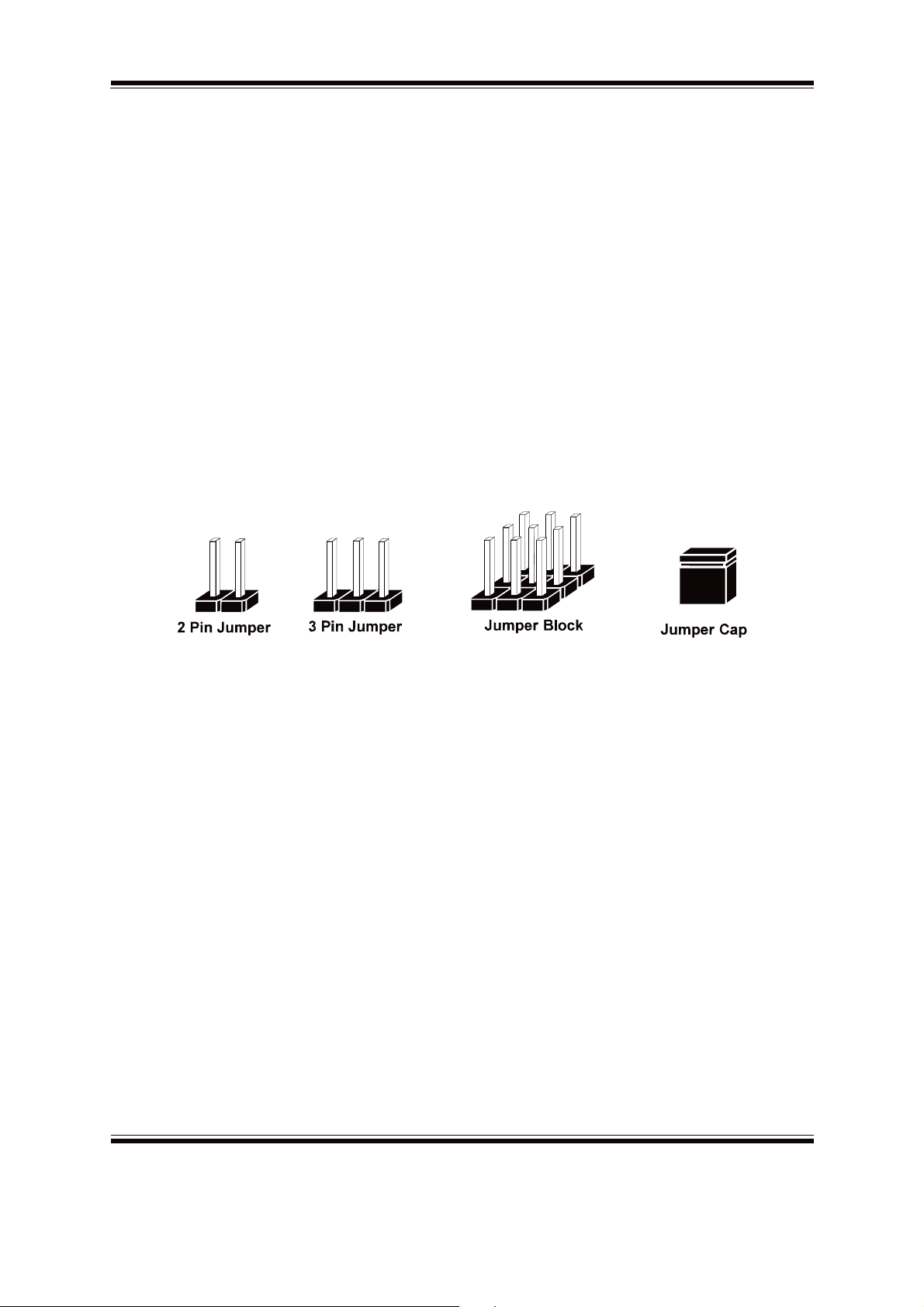
2-3. HOW TO SET THE JUMPERS
You can configure your board by setting jumpers. Jumper is consists of two or three
metal pins with a plastic base mounted on the card, and by using a small plastic "cap",
Also known as the jumper cap (with a metal contact inside), you are able to connect
the pins. So you can set-up your hardware configuration by "open" or "close" pins.
The jumper can be combined into sets that called jumper blocks. When the jumpers
are all in the block, you have to put them together to set up the hardware configuration.
The figure below shows how this looks like.
JUMPERS AND CAPS
If a jumper has three pins (for examples, labelled PIN1, PIN2, and PIN3), You can
connect PIN1 & PIN2 to create one setting by shorting. You can either connect PIN2
& PIN3 to create another setting. The same jumper diagrams are applied all through
this manual. The figure below shows what the manual diagrams look and what they
represent.
Page: 2-5

Chapter 2 Hardware Configuration
JUMPER DIAGRAMS
Jumper Cap
looks like this
2 pin Jumper
looks like this
3 pin Jumper
looks like this
JUMPER SETTINGS
1
1
1
2
Jumper Block
looks like this
2 pin Jumper close(enabled)
Looks like this
3 pin Jumper
2-3 pin close(enabled)
Looks like this
Jumper Block
1-2 pin close(enabled)
Looks like this
1
1
12
Page: 2-6
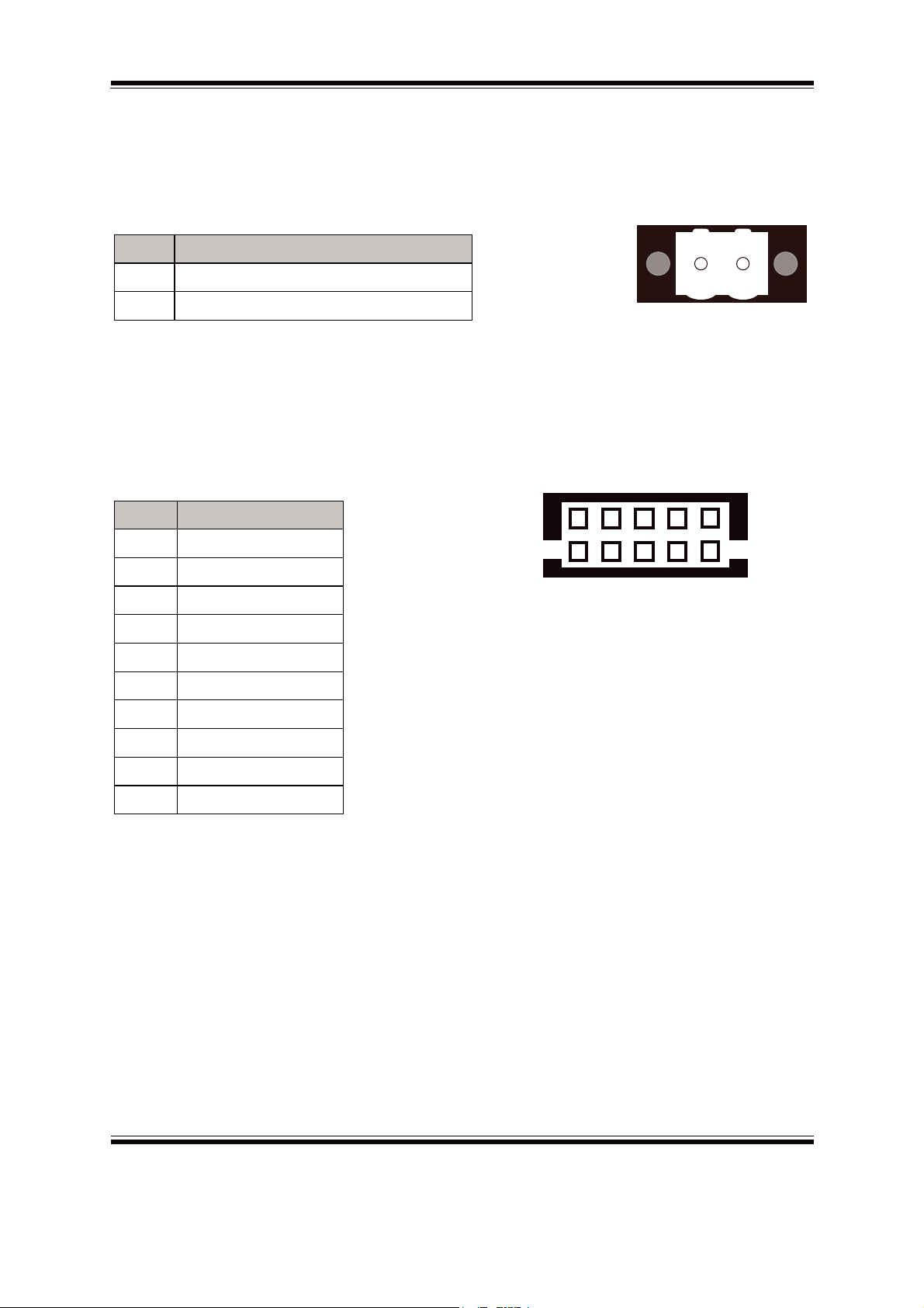
2-4. PWR IN CONNECTOR
CN_POWER1: PWR IN Connector
The pin assignments are as follows:
PIN ASSIGNMENT
Chapter 2 Hardware Configuration
1 PWRI(9~36V)ġ
2 GND
2-5.COM PORT & CONNECTOR
COM1: COM1 Connectors
The pin assignments are as follows:
PIN ASSIGNMENT
1
2
3
4
5
6
7
DCD1
RXD1
TXD1
DTR1
GND
DSR1
RTS1
12
&1B32:(5
6
10
51
&20&20&20
&20&20&20
8
9
10
CTS1
RI selectable
NC
Page: 2-7

Chapter 2 Hardware Configuration
COM1, COM2, COM3,COM4,COM5,COM6: COM Connectors
The pin assignments are as follows:
COM1:
PIN ASSIGNMENT PIN ASSIGNMENT
1 COM1_DCD_C 6 COM1_DSR_C
2 COM1_RX_C 7 COM1_RTS_C
3 COM1_TX_C 8 COM1_CTS_C
4 COM1_DTR_C 9 RI/+5V/+12 selectable
5 GND 10 NC
COM2:
PIN ASSIGNMENT PIN ASSIGNMENT
1 COM2_DCD_C 6 COM2_DSR_C
2 COM2_RX_C 7 COM2_RTS_C
3 COM2_TX_C 8 COM2_CTS_C
4 COM2_DTR_C 9 RI/+5V/+12 selectable
5 GND 10 NC
COM3:
PIN ASSIGNMENT PIN ASSIGNMENT
1 COM3_DCD_C 6 COM3_DSR_C
2 COM3_RX_C 7 COM3_RTS_C
3 COM3_TX_C 8 COM3_CTS_C
4 COM3_DTR_C 9 COM3_RI_C
5 GND 10 NC
COM4:
PIN ASSIGNMENT PIN ASSIGNMENT
1 COM4_DCD_C 6 COM4_DSR_C
2 COM4_RX_C 7 COM4_RTS_C
3 COM4_TX_C 8 COM4_CTS_C
4 COM4_DTR_C 9 COM4_RI_C
5 GND 10 NC
Page: 2-8

Chapter 2 Hardware Configuration
COM5:
PIN ASSIGNMENT PIN ASSIGNMENT
1 COM5_DCD_C 6 COM5_DSR_C
2 COM5_RX_C 7 COM5_RTS_C
3 COM5_TX_C 8 COM5_CTS_C
4 COM5_DTR_C 9 COM5_RI_C
5 GND 10 NC
COM6:
PIN ASSIGNMENT PIN ASSIGNMENT
1 COM6_DCD_C 6 COM6_DSR_C
2 COM6_RX_C 7 COM6_RTS_C
3 COM6_TX_C 8 COM6_CTS_C
4 COM6_DTR_C 9 COM6_RI_C
5 GND 10 NC
Note: COM1/2 connectors are selectable for RI, +5V or
+12V.For more information, please refer to COM
PORT & VOLTAGE SELECTION.
Page: 2-9
Chapter 2 Hardware Configuration
2-6. COM PORT RI & VOLTAGE SELECTION
JPCOM1, JPCOM2: COM Port RI & Voltage Selection
The jumper settings are as follows:
SELECTION JUMPER
SETTING
RI
1-2
(default)
VCC12 3-4
VCC5V 5-6
JUMPER ILLUSTRATION
2
1
-3&20
2
1
-3&20
2
1
6
5
6
5
6
5
2
1
-3&20
2
1
-3&20
2
1
6
5
6
5
6
5
Note: The manufacturing default is RI
2-7.USB Connector
USB2: Internal USB Connector
The pin assignment is as follows:
PIN ASSIGNMENT
1 VCC5V
2 USBC2N
3 USBC2P
4 GND
5 GND
-3&20
-3&20
4
1
86%
Page: 2-10
USB3: Internal USB Connector
The pin assignment is as follows:
PIN ASSIGNMENT
Chapter 2 Hardware Configuration
1 VCC5V
2 USBC3N
3 USBC3P
4 GND
5 GND
USB4: Internal USB Connector
The pin assignment is as follows:
PIN ASSIGNMENT
1 VCC5V
2 USBC4N
3 USBC4P
4 GND
5 GND
86%
86%
USB5: Internal USB3.0 Connector
The pin assignment is as follows:
PIN ASSIGNMENT
1 VCC5V
2 USBB_DM
3 USBB_DP
4 GND
5 U3RXNDN1
6 U3RXNDP1
7 GND
8 U3TXDN1
9 U3TXDP1
9
1
86%
Page: 2-11
5
4

Chapter 2 Hardware Configuration
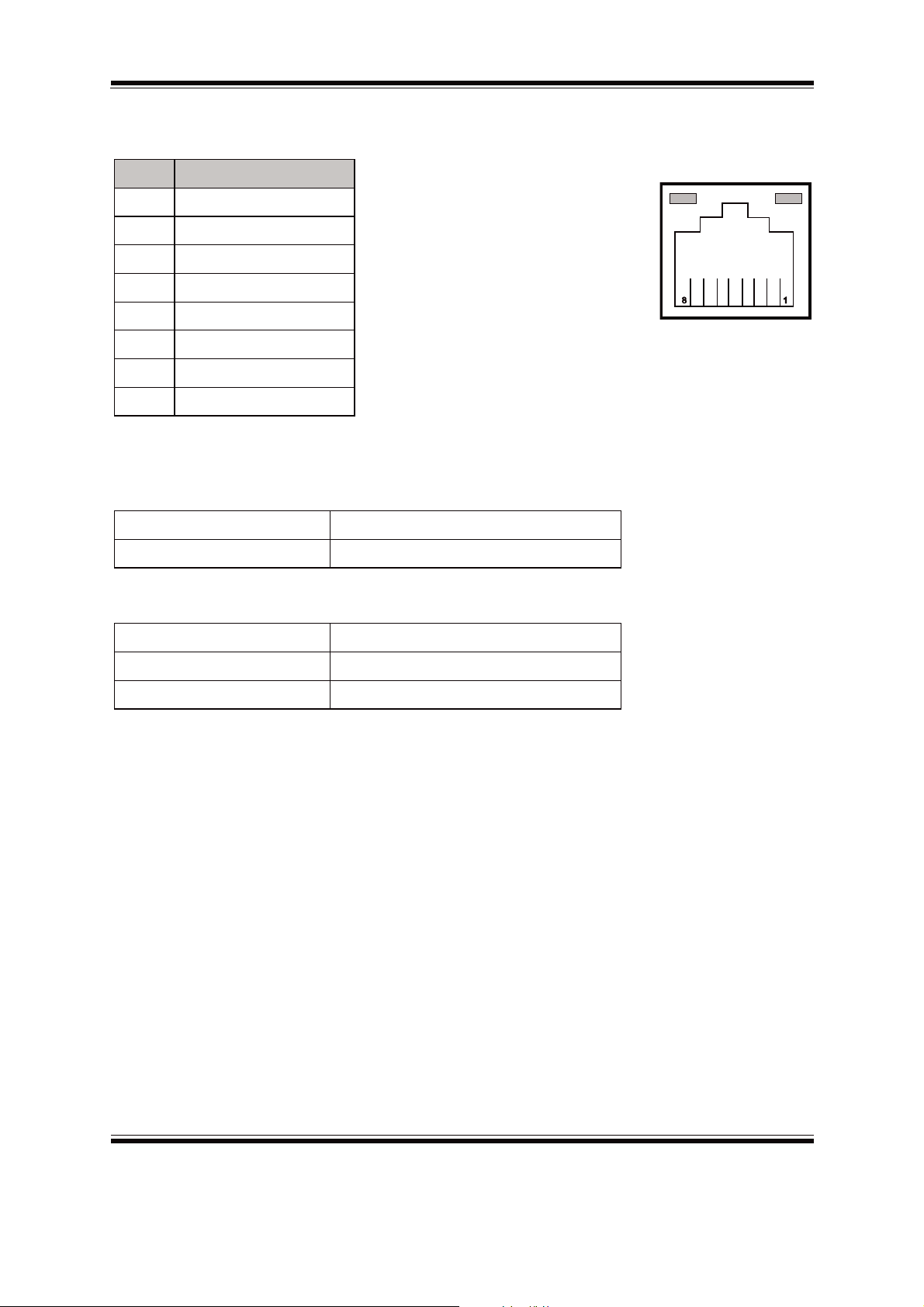
2-8. LAN PORT
LAN1: LAN Connectors
The pin assignments are as follows:
PIN ASSIGNMENT
1
2
3
4
5
6
7
8
MDI_0P
MDI_0N
MDI_1P
MDI_1N
MDI_2P
MDI_2N
MDI_3P
MDI_3N
LAN LED Indicator:
Left Side LED
Green Color Blinking LAN Message Active
Off No LAN Message Active
*UHHQ 2UDQJH
/$1
Right Side LED
Orange Color On 10/100 LAN Speed Indicator
Red Color On Giga LAN Speed Indicator
Off No LAN switch/ hub connected.
Page: 2-12
LAN2: LAN Connectors
The pin assignments are as follows:
PIN ASSIGNMENT
1
MDI_0P
Chapter 2 Hardware Configuration
*UHHQ 2UDQJH
2
3
4
5
6
7
8
MDI_0N
MDI_1P
MDI_1N
MDI_2P
MDI_2N
MDI_3P
MDI_3N
LAN LED Indicator:
Left Side LED
Green Color Blinking LAN Message Active
Off No LAN Message Active
Right Side LED
Orange Color On 10/100 LAN Speed Indicator
Red Color on Giga LAN Speed Indicator
/$1
Off No LAN switch/ hub connected.
Page: 2-13
Chapter 2 Hardware Configuration
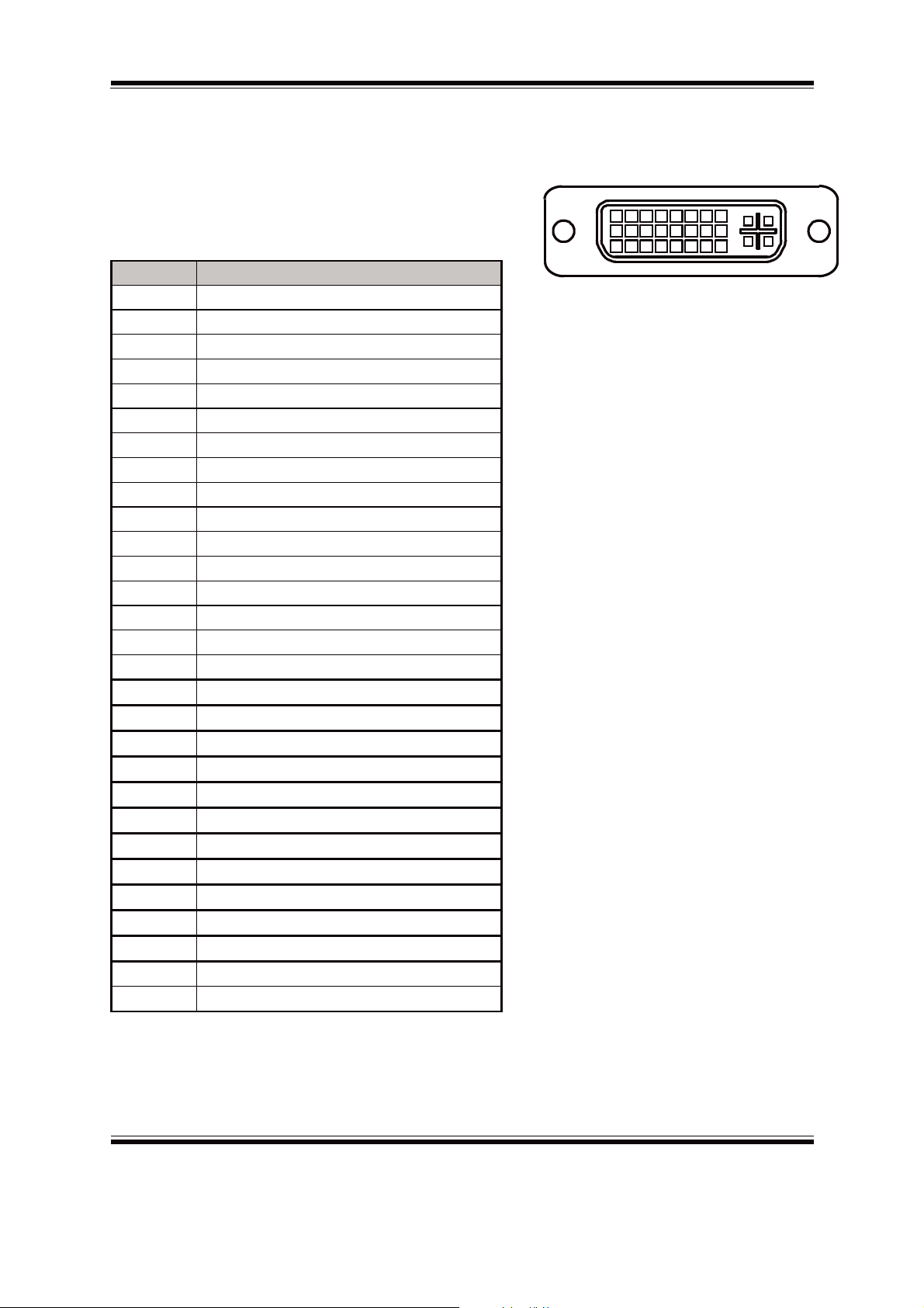
2-9. DVI CONNECTOR
DVI2: DVI-I Connector
The pin assignment is as follows:
PIN ASSIGNMENT
1 DVI_22 DVI_2+
3 GND
4 NC
5 NC
6 DVI_clock
7 DVI_data
8 CRT_VSYNC
9 DVI_110 DVI_1+
11 GND
12 NC
13 NC
14 VCC
15 GND
16 DVI_HPD
17 DVI_018 DVI_0+
19 GND
20 NC
21 NC
22 GND
23 DVI_Clock+
24 DVI_Clock-
C1 CRT_RED
C2 CRT_GREEN
C3 CRT_BLUE
C4 CRT_HSYNC
C5 GND
17
C1 C2
1
9
C3 C5 C4
'9,
Page: 2-14

DVI1: DVI-D Connector
The pin assignment is as follows:
Chapter 2 Hardware Configuration
PIN ASSIGNMENT
1 DVI_2-
2 DVI_2+
3 GND
4 NC
5 NC
6 DVI_clock
7 DVI_data
8 NC
9 DVI_110 DVI_1+
11 GND
12 NC
13 NC
14 VCC
15 GND
16 DVI_HPD
17 DVI_018 DVI_0+
19 GND
20 NC
21 NC
22 GND
23 DVI_Clock+
24 DVI_Clock-
C1 NC
C2 NC
C3 NC
C4 NC
C5 NC
17
C1 C2
1
9
C3 C5 C4
'9,
Page: 2-15

Chapter 2 Hardware Configuration
2-10. DIGITAL I/O CONNECTOR
DIO1: Digital I/O Connector.
The pin assignments are as follows:
PIN ASSIGNMENT PIN ASSIGNMENT
1 DIN0 2 GND
3 DIN1 4 GND
5 DIN2 6 V5_SB
7 DIN3 8 GND
9 DOUT0 10 GND
11 DOUT1 12 GND
13 DOUT2 14 GND
15 DOUT3
JDIO1: Digital I/O Connector.
The pin assignments are as follows:
15
610
1115
',2
PIN ASSIGNMENT PIN ASSIGNMENT
1 V5_SB 2 GND
3 DIN1 4 DOUT1
5 DIN2 6 DOUT2
7 DIN3 8 DOUT3
9 DIN4 10 DOUT4
910
-',2
Page: 2-16
2-11. AUDIO CONNECTOR
JAUDIO1: Audio Connectors
The pin assignments are as follows:
PIN ASSIGNMENT
1
2
3
4
5
MIC1L
MIC1R
GND
GND
LINEINL
Chapter 2 Hardware Configuration
2
10
91
-$8',2
6
7
8
9
10
LINEINR
GND
GND
LINEOUTL
LINEOUTR
Page: 2-17
Chapter 2 Hardware Configuration
2-12. SATA & SATA POWER CONNECTOR
SATA1: Serial ATA Connector
The pin assignments are as follows:
PIN ASSIGNMENT
1
2
3
4
5
6
7
GND
TX+
TX-
GND
RX-
RX+
GND
HDD_Power1: Serial ATA Power Connector
The pin assignments are as follows:
PIN ASSIGNMENT
1
2
VCC5V
GND
6$7$
12
+''B32:(5
Page: 2-18
2-13. CFAST CARD SLOT
CFAST1: CFAST Card Slot
The pin assignments are as follows:
Chapter 2 Hardware Configuration
PIN ASSIGNMENT PIN ASSIGNMENT
S1 GND PC6 NC
S2 SATA_TXP0 PC7 GND
S3 SATA_TXN0 PC8 NC
S4 GND PC9 NC
S5 SATA_RXN0 PC10 NC
S6 SATA_RXP0 PC11 NC
S7 GND PC12 NC
PC1 NC PC13 3.3V/5V
PC2 GND PC14 3.3V/5V
PC3 NC PC15 GND
PC4 NC PC16 GND
PC5 NC PC17 NC
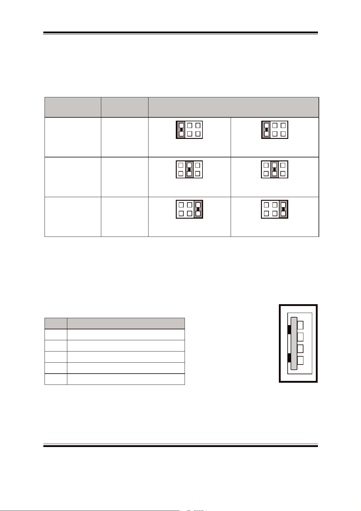
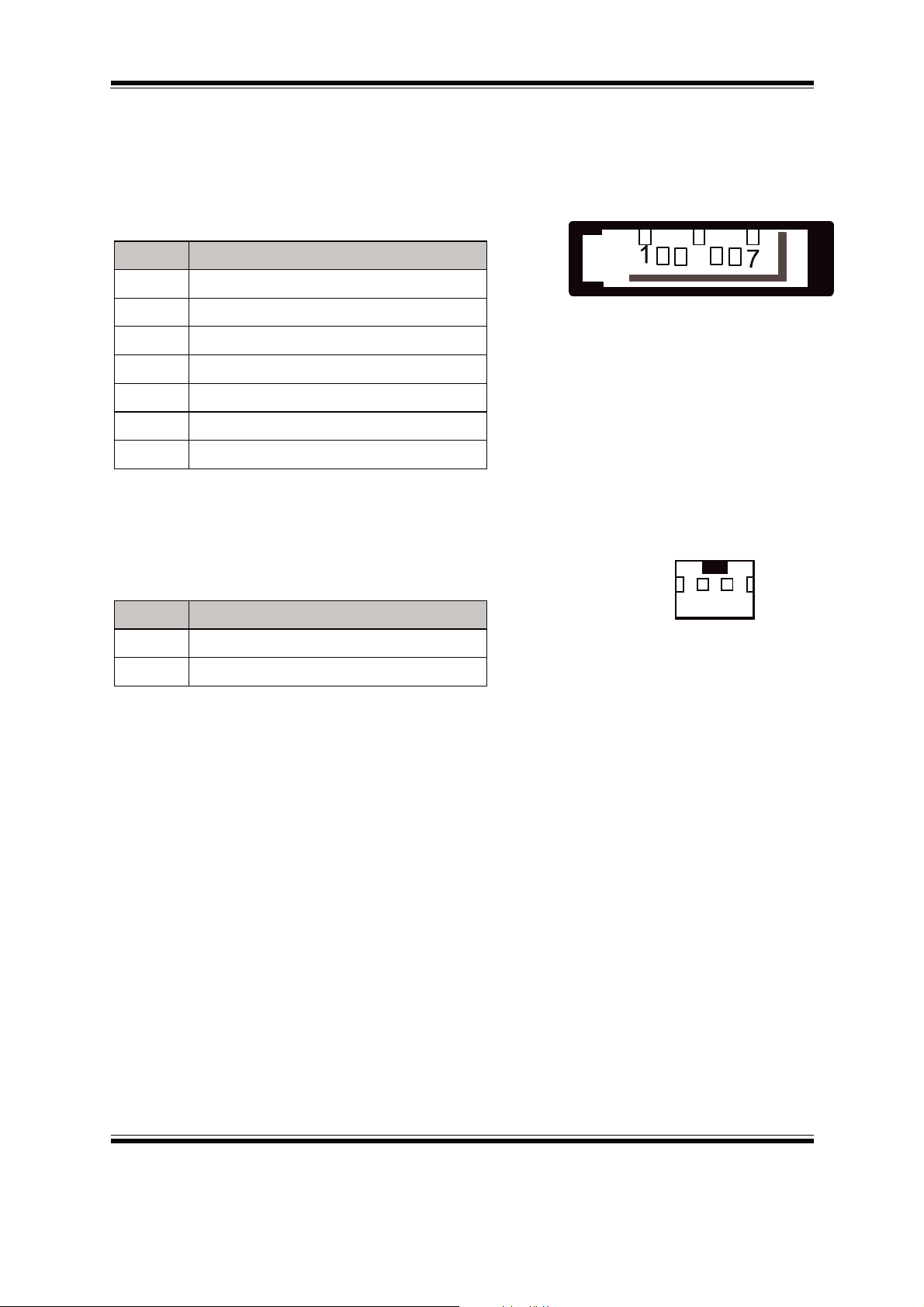
2-14. CFAST CARD POWER SELECTIONġġġġ
JP11: CFAST Card Power Connector
The selections are as follows:
S7
S1
PC1 PC17
&)$67
SELECTION JUMPER SETTINGS JUMPER ILLUSTRATION
1
3.3V 1-2
3
-3
1
5V 2-3
3
-3
Note: Manufacturing Default is 3.3V
Page: 2-19

Chapter 2 Hardware Configuration
2-15. Clear CMOS DATA SELECTION
JP1: Clear CMOS Data Selection Connector
The selections are as follows:
SELECTION JUMPER SETTINGS JUMPER ILLUSTRATION
Normal
(default)
Clear CMOS 1-2
Note: Manufacturing Default is normal
1-X
2-16. DVI-D ENABLE SELECTION
JP34/JP35: DVI-D Enable Selection
The selections are as follows:
SELECTION
JUMPER SETTING JUMPER ILLUSTRATION
1
-3
1
-3
13
DVI-D Enable
(Default)
DVI-D Disable 2-3
Note: Manufacturing Default is DVI-D Enable
Page: 2-20
1-2
13
-3-3
13
13
-3-3

Chapter 2 Hardware Configuration
2-17. DVI-D HPD ENABLE SELECTION
JP37: DVI-D HPD Enable Selection
The selections are as follows:
SELECTION
DVI-D HPD
Enable
(default)
DVI-D HPD
Disable
Note: Manufacturing Default is DVI-D HPD Enable
JUMPER SETTING JUMPER ILLUSTRATION
1-2
1-x
2-18. DDC SELECTION
JP13: DDC Selection
The selections are as follows:
12
-3
12
-3
SELECTION
VGA DDC
DVI-I DDC
Note: 1. Manufacturing default is DVI-DDC.
2. Please set JP13 to VGA DDC if connecting VGA & DVI-D as dual display
JUMPER SETTING JUMPER ILLUSTRATION
1-2
4-6
1-3
5-6
21
65
-3
21
5
6
-3
Page: 2-21

SOFTWARE
UTILITIES
This chapter comprises the detailed information of VGA driver, LAN
driver, and Sound driver.
Section includes:
z Introduction
z Intel
z Intel ® Trusted Execution Engine Driver installation
z Intel ® Kernel-Mode Driver Framework Driver installation
z Intel® Mailbox Interface Device Driver installation
z VGA Driver Utility
z LAN Driver Utility
z SOUND Driver Utility
z For USB3.0 Driver installation
®
Chipset Software Installation Utility
CHAPTER
3
Page: 3-1

Chapter 3 Software Utilities
3-1. INTRODUCTION
Enclosed with our E/ package, you will find a DVD ROM disk containing all
types of drivers we have. As a user, you will only need some of files
contained in the DVD ROM disk, please take note of the following chart:
FILENAME
PURPOSE
(Assume that DVD ROM drive is D :)
D:\Driver\Platform\Win7, Win8.1(32-bit)\Main Chip
or
Intel ® Chipset Software
Installation Utility
D:\Driver\Platform\Win7, Win8.1(64-bit)\Main Chip
D:\Driver\Platform\ Win7, Win8.1 (32-bit)\TXE
or
Intel ® Trusted Execution
Engine Driver installation
D:\Driver\Platform\ Win7, Win8.1(64-bit)\TXE
D:\Driver\Platform\Win7(32/64-bit)\KMDF Intel ® Kernel-Mode Driver
Framework Driver
installation
D:\Driver\Platform\Win8.1 (32/64-bit)\MBI Intel® Mailbox Interface
Device Driver installation
D:\Driver\Platform\ Win7, Win8.1 (32-bit)\VGA
or
D:\Driver\Platform\ Win7, Win8.1(64-bit)\VGA
Intel ® Atom ™ Processor
E3800 Series Driver
installation
D:\Driver\Platform\ Win7, Win8.1 (32-bit)\LAN
or
D:\Driver\Platform\ Win7, Win8.1(64-bit)\LAN
D:\Driver\Platform\ Win7, Win8.1 (32-bit)\Sound
or
WGI210IT Intel® Springville
GbE Controller for LAN
Driver installation
Realtek ® ALC888S for
Sound Driver installation
D:\Driver\Platform\ Win7, Win8.1(64-bit)\Sound
D:\Driver\Device\Platform\Win7(32/64-bit)USB3.0 For USB3.0 Driver
installation
D:\Driver\Device Driver installation for Card
Reader , wireless, 3G, etc.
D:\Driver\FLASH
Driver installation for BIOS
update utility (AMI)
Note: Be sure to install the Utility right after the OS is fully installed.
Page:3-2

Chapter 3 Software Utilities
3-2. INTEL® CHIPSET SOFTWARE INSTALLATION UTILITY
3-2-1. Introduction
The Intel
These files outline to the operating system how to configure the Intel
components in order to ensure that the following features function properly:
x PCIe Support
x SATA Storage Support
x USB Support
x Identification of Intel
3-2-2. Installation of Utility for Windows 7/ 8.1
®
Chipset Device Software installs Windows *.INF files to the target system.
®
Chipset Components in the Device Manager
®
chipset
The Utility Pack is made only for Windows 7/ 8.1. It should be installed right after the
OS installation; kindly follow the following steps:
1. Place insert the Utility Disk into Floppy Disk Drive A/B or DVD ROM drive.
2. Under Windows system, go to the directory where Utility Disc is located.
e.g.: \DRIVER\UTILITY\infinst_autol.exe
3. Click infinst_autol.exe file for utility installation.
4. Follow the instructions on the screen to complete the installation.
5. Once installation is completed, shut down the system and restart in order for the
changes to take effect.
Page:3-3

Chapter 3 Software Utilities
3-3. INTEL® TRUSTED EXECUTION ENGINE DRIVER
INSTALLATION
3-3-1. Introduction
The Intel® ME software components that need to be installed depend on the system's
specific hardware and firmware features. The installer, compatible with Windows 7/
8.1, detects the system's capabilities and installs the relevant drivers and applications.
3-3-2. Installation Instructions for Windows 7/ 8.1
1. Insert the driver disk into a DVD ROM device.
2. Under Windows system, go to the directory where the driver is located.
3. Run the application with administrative privileges.
Page:3-4

Chapter 3 Software Utilities
3-4. INTEL ® KERNEL-MODE DRIVER FRAMEWORK DRIVER
INSTALLATION
3-4-1. Introduction
The Intel ® Kernel-Mode Driver Framework Driver that needs to be installed depends
on the system's specific hardware and firmware features. The installer, compatible
with Windows 7/ 8.1, detects the system's capabilities and installs the relevant drivers
and applications.
3-4-2. Installation Instructions for Windows 7
To install the utility, simply follow the following steps:
1. Insert the driver disk into a DVD ROM device.
2. Under Windows system, go to the directory where the driver is located.
3. Run the application with administrative privileges.
Page:3-5

Chapter 3 Software Utilities
3-5. INTEL® MAILBOX INTERFACE DEVICE DRIVER
3-5-1. Introduction
The Intel® Mailbox Interface Device Driver is a bridge to the Intel Dynamic Platform
and Thermal Framework. It needs to be installed depend on the system's specific
hardware and firmware features. The installer, compatible with Windows 8.1, detects
the system's capabilities and installs the relevant drivers and applications. The driver
supports the following Intel
Intel® Bay Trail –M Platforms with ValleyView2 SOC.
3-5-2. Installation Instructions for Windows 8.1
®
Chipsets/Processors:
To install the utility, simply follow the following steps:
4. Insert the driver disk into a DVD ROM device.
5. Under Windows system, go to the directory where the driver is located.
6. Run the application with administrative privileges.
Page:3-6

Chapter 3 Software Utilities
3-6. INTEL® USB3.0 EXTENSIBLE HOST CONTROLLER
UTILITY
3-6-1. Introduction
Intel® USB 3.0 eXtensible Host Controller Driver supports the following Intel®
Chipsets/Processors:
Intel
Intel
Intel
® 4th
Generation Core™ Processor Family
®
8 Series/C220 Series Chipset Family
® 4th
Generation U-Series Platform I/O
3-6-2. Installation Instructions for Windows 7
To install the utility, simply follow the following steps:
7. Insert the driver disk into a DVD ROM device.
8. Under Windows system, go to the directory where the driver is located.
9. Run the application with administrative privileges.
Page:3-7

Chapter 3 Software Utilities
3-7. VGA DRIVER UTILITY
The VGA interface is embedded with our E/ system to support CRT display.
The following illustration briefly shows you the content of VGA driver in
D:\Driver\VGA.
Win7Series
Win 8.1
3-7-1. Installation of VGA Driver
1. Start the computer (Win 7).
2. Insert the Utility Disk into the DVD ROM drive or drive A/B.
3. Open the VGA folder for your system to choose an appropriate folder, and
double-click "exe" file to install. e.g. d:\DRIVER\VGA\Your system\ ***.exe
(If D is not your DVD-ROM drive, substitute D with the correct drive letter.)
4. Follow the Wizard's on-screen instructions to complete the installation.
Page:3-8

Chapter 3 Software Utilities
3-8 LAN DRIVER UTILITY
The EL1083 is enhanced with LAN function that can support various network
adapters. The content of the LAN driver is found as follows:
Win 7 Series
Win 8.1
For more details on Installation procedure, please refer to Readme.txt file
found on LAN DRIVER UTILITY.
Page:3-9

Chapter 3 Software Utilities
3-9. SOUND DRIVER UTILITY
3-9-1. Introduction
The Audio chip enhanced in this system is fully compatible with Windows 7/ 8.1.
Below, you will find the content of the Sound driver:
Win 7 Series
Win 8.1
3-9-2. Installation Procedure for Windows 7/ 8.1
1. Open the SOUND folder. For your system to choose an appropriate folder, and
Run the setup.exe program to start the installation. e.g. :\DRIVER\SOUND\Your
system\setup.exe
2. (If D is not your DVD-ROM drive, substitute D with the correct drive letter.)
3. Click on [Next] to continue the procedure. If the Windows popup "Windows
can't verify the publisher of this driver software" message, press "Install this
driver software anyway" to continue the installation.
4. Finally, select to restart the system and press [Finish] to complete the installation.
Page:3-10

SYSTEM
INSTALLATION
This chapter shows how to install system for EL1083.
Section includes:
CHAPTER
4
z Removing the bottom case
z HDD Installation
z SO-DIMM Installation
z Wireless LAN or 3G module Installation
z CFast Card Installation
z PoE Board Installation
Page: 4-1

Chapter 4 System Installation
4.1 Removing the bottom case
Caution:
Please make sure the system is powered off and disconnected from the power sources
before removing the bottom case to prevent electric shock or system damage.
1. Locate the 6 screws on the bottom case
Page:4-2

2. Remove the 6 screws on the bottom case
Chapter 4 System Installation
3. Remove the bottom case
Page:4-3

Chapter 4 System Installation
4.2. HDD Installation
1. Remove the bottom case
2. Remove the 2 screws of HDD drive bay
Page:4-4

3. Paste thermal pad on HDD PCB (drive bay side)
Chapter 4 System Installation
4. Put the HDD on the drive bay correctly
Page:4-5

Chapter 4 System Installation
5. Fasten 4 HDD screws to fix HDD on the drive bay
6. Plug SATA & HDD power cables on the mother board
Page:4-6

Chapter 4 System Installation
7. Plug SATA & HDD power cable into HDD and put HDD & drive bay on the
chassis
8. Fasten the 2 screws of HDD drive bay
Page:4-7

Chapter 4 System Installation
4.3. SO-DIMM Installation
1. Remove the bottom case
2. Remove the 2 screws & SATA/power cables of HDD drive bay
Page:4-8

3. Remove SATA/power cables on the mother board
Chapter 4 System Installation
4. Locate the SO-DMM socket
SO-DIMM
Page:4-9

Chapter 4 System Installation
5. Prepare SO-DIMM and SO-DIMM heatsinks
6. Paste SO-DIMM heatsinks on the 2 sides of SO-DIMM
Page:4-10

Chapter 4 System Installation
7. Insert the SO-DIMM into the socket at 20~30 degrees angle
8. Gently push the rear of the SO-DIMM down until it’s clipped into place and
secure the SO-DIMM in the socket.
Page:4-11

Chapter 4 System Installation
4.4. Wireless LAN or 3G module Installation
A. Full-size mini-PCIe slot
1. If a half-size mini-PCIe module, connect it with half-size to full-size mini-PCIe
bracket by 2 screws before installation
2. Locate the full size mini-PCIe slot
Page:4-12

Chapter 4 System Installation
3. Insert the mini-PCIe module into the full-size mini-PCIe slot
Figure 3a. Half-size mini-PCIe module
Figure3b. Full-size mini-PCIe module
Page:4-13

Chapter 4 System Installation
4. Fasten the 2 screws of full-size mini-PCIe slot
Figure 4a. Half-size mini-PCIe module
Figure 4b. Half-size mini-PCIe module
Page:4-14

B. Half-size mini-PCIe slot
1. Locate the half size mini-PCIe slot
Chapter 4 System Installation
2. Insert the mini-PCIe module into the half-size mini-PCIe slot
Page:4-15

Chapter 4 System Installation
3. Fasten the 2 screws of half-size mini-PCIe slot
Page:4-16

4.5. CFast Card Installation
1. Remove the bottom case
Chapter 4 System Installation
2. Remove HDD drive bay & SATA/power cable
Page:4-17

Chapter 4 System Installation
3. Remove PoE LED cable on PoE board (skip item 3~5 if no PoE board)
4. Remove 2 screws of PoE board
Page:4-18
5. Remove PoE board from connector
Chapter 4 System Installation
6. Locate the Cfast Card slot
Page:4-19

Chapter 4 System Installation
7. Put the Cfast card in the slot
8. Push Cfast card to the end of slot
Page:4-20

4.6. PoE Board Installation
1. Connect the PoE LED cable on PoE board
Chapter 4 System Installation
2. Put PoE board right on the PoE connector
Page:4-21

Chapter 4 System Installation
3. Fasten 2 screws of PoE board
Page:4-22

AMI
BIOS SETUP
This chapter shows how to set up the AMI BIOS.
Section includes:
z Introduction
CHAPTER
5
z Entering Setup
z Main
z Advanced
z Chipset
z Boot
z Security
z Save & Exit
Page: 5-1

h
o
d
P
t
i
i
r
a
d
l
e
i
5.1 Introduction
C
apter 5 AMI BIOS SETUP
The board uses an AMI Aptio BIOS that is st
red in the Serial Peripheral
Interface Flash Memory (SPI Flash) and can be update
BIOS Setup program, Power-on Self-Test (POST), the
LAN EEPROM information, and Plug and Play suppor
Aptio is AMI’s BIOS firmware based on the UEFI (Un
Interface) Specifications and the Intel Platform Innovat
UEFI specification defines an interface between an ope
firmware. The interface consists of data tables that cont
information, boot service calls, and runtime service call
operating system and its loader. These provide standar
operating system and running pre-boot applications. Fo
Extensible Firmware Interface’s position in the softwar
. The SPI Flash contains the
CI auto-configuration utility,
.
fied Extensible Firmware
on Framework for EFI. The
ating system and platform
in platform-related
s that are available to the
environment for booting an
lowing illustration shows
stack.
EFI BIOS provides an user interface allow users the ab
configuration, e.g. change system date and time, enable
Page:5-2
lity to modify hardware
or disable a system

Chapter 5 AMI BIOS SETUP
component, decide bootable device priorities, setup personal password, etc., which is
convenient for modifications and customization of the computer system and allows
technicians another method for finding solutions if hardware has any problems.
The BIOS Setup program can be used to view and change the BIOS settings for the
computer. The BIOS Setup program is accessed by pressing the <Del> or <ESC> key
after the POST memory test begins and before the operating system boot begins. The
settings are shown below.
Page:5-3

Chapter 5 AMI BIOS SETUP
5.2 Entering Setup
When the system is powered on, the BIOS will enter the Power-On Self Test
(POST) routines and the following message will appear on the lower screen:
BIOS POST Screen
As long as this message is present on the screen you may press the <Del> key to
access the Setup program. In a moment, the main menu of the Aptio Setup Utility
will appear on the screen:
Page:5-4

Chapter 5 AMI BIOS SETUP
Setup program initial screen
You may move the cursor by up/down keys to highlight the individual menu items.
As you highlight each item, a brief description of the highlighted selection will appear
at the bottom of the screen.
Page:5-5

5.3 Main
Chapter 5 AMI BIOS SETUP
Main Screen
BIOS Setting Options Description/Purpose
BIOS Vendor No changeable
options Displays the BIOS vendor.
Core Version No changeable
options
Compliancy No changeable
options Displays the current UEFI version.
Project Version No changeable
options
Build Date and Time No changeable Displays the date of current BIOS
Displays the current BIOS core
version.
Displays the version of the BIOS
currently installed on the platform.
Page:5-6

options version.
Total Memory No changeable
options Displays the memory size.
Intel(R) GOP Driver No changeable
options Displays the GOP driver version.
Chapter 5 AMI BIOS SETUP
Sec RC Version No changeable
options
TXE Firmware
Version
No changeable
options Displays the current TXE Version
Displays the current Sec RC
version.
System Language English BIOS Setup language.
System Date month, day, year Specifies the current date.
System Time hour, minute, second Specifies the current time.
Page:5-7

5.4 Advanced
Chapter 5 AMI BIOS SETUP
Advanced Screen
BIOS Setting Options Description/Purpose
ACPI Settings Sub-Menu System ACPI Parameters.
F81866 SuperIO
Configuration
Hardware Monitor Sub-Menu Monitor hardware status
F81866 MISC Sub-Menu F81866 relation function.,
CPU Configuration Sub-Menu CPU Configuration. Parameters.
PPM Configuration Sub-Menu PPM Configuration. Parameters.
Sub-Menu System Super IO Chip
Configuration.
Page:5-8

Chapter 5 AMI BIOS SETUP
IDE Configuration Sub-Menu SATA Configuration Parameters.
OS Selection Sub-Menu OS selection settings.
LPSS & SCC
Configuration
Sub-Menu LPSS & SCC Configuration
Setting
CSM Configuration Sub-Menu Configure Option ROM
execution, boot options filters,
etc..
USB Configuration Sub-Menu USB Configuration Parameters.
Page:5-9

h
p
s
s
e
p
o
5.4.1 Advanced –ACPI Settings
C
apter 5 AMI BIOS SETUP
ACPI Settings Screen
BIOS Setting Options Descri
Enable ACPI
Auto
Configuration
Enable
Hibernation
- Disabled
- Enabled
- Disabled
- Enabled
Enable
Enable
to Hib
This o
with s
tion/Purpose
or Disables ACPI feature.
or Disables System ability
rnate (OS/S4 Sleep State).
tion may be not effective
me OS.
Page:5-10

Chapter 5 AMI BIOS SETUP
ACPI Sleep State - Suspend Disabled
- S3 Only (Suspend to
RAM)
Specifies the ACPI sleep state.
Suspend Disabled disables ACPI
sleep feature.
S3 allows the platform to enter
Suspend to RAM mode.
Page:5-11

Chapter 5 AMI BIOS SETUP
5.4.2 Advanced - F81866 Super IO Configuration
Super IO Configuration Screen
BIOS Setting Options Description/Purpose
Super IO Chip No changeable options Displays the super IO chip
model and its manufacturer.
Serial Port 1
Configuration
Serial Port 2
Configuration
Serial Port 3
Configuration
Sub-menu Set Parameters for COMA
Sub-menu Set Parameters for COMB
Sub-menu Set Parameters for COMC
Page:5-12

Chapter 5 AMI BIOS SETUP
Serial Port 4
Configuration
Serial Port 5
Configuration
Serial Port 6
Configuration
Sub-menu Set Parameters for COMD
Sub-menu Set Parameters for COME
Sub-menu Set Parameters for COMF
Page:5-13

Chapter 5 AMI BIOS SETUP
Serial Port 1 Configuration Screen
BIOS Setting Options Description/Purpose
Serial Port -Disabled
-Enabled
Device Settings No changeable options Displays current settings of
Change Settings -Auto
-IO=3F8h; IRQ=4
-IO=3F8h;
IRQ=3,4,5,6,7,9,10,11,12
-IO=2F8h;
IRQ=3,4,5,6,7,9,10,11,12
Enable or disable serial port
1.
serial port 1.
Select IRQ and I/O
resource for the serial port
1.
Page:5-14

Chapter 5 AMI BIOS SETUP
-IO=3E8h;
IRQ=3,4,5,6,7,9,10,11,12
-IO=2E8h;
IRQ=3,4,5,6,7,9,10,11,12
Page:5-15

Chapter 5 AMI BIOS SETUP
Serial Port 2 Configuration Screen
BIOS Setting Options Description/Purpose
Serial Port -Disabled
-Enabled
Device Settings No changeable options Displays current settings of
Change Settings -Auto
-IO=2F8h; IRQ=3
-IO=3F8h;
IRQ=3,4,5,6,7,9,10,11,12
-IO=2F8h;
IRQ=3,4,5,6,7,9,10,11,12
Enable or disable serial port
2.
serial port 2.
Select IRQ and I/O
resource for the serial port
2.
Page:5-16

Chapter 5 AMI BIOS SETUP
-IO=3E8h;
IRQ=3,4,5,6,7,9,10,11,12
-IO=2E8h;
IRQ=3,4,5,6,7,9,10,11,12
Page:5-17

Chapter 5 AMI BIOS SETUP
Serial Port 3 Configuration Screen
BIOS Setting Options Description/Purpose
Serial Port -Disabled
-Enabled
Device Settings No changeable options Displays current settings of
Change Settings -Auto
-IO=3E8h; IRQ=7
-IO=3F8h;
IRQ=3,4,5,6,7,9,10,11,12
-IO=2F8h;
IRQ=3,4,5,6,7,9,10,11,12
Enable or disable serial port
3.
serial port 3.
Select IRQ and I/O
resource for the serial port
3.
Page:5-18

Chapter 5 AMI BIOS SETUP
-IO=3E8h;
IRQ=3,4,5,6,7,9,10,11,12
-IO=2E8h;
IRQ=3,4,5,6,7,9,10,11,12
Page:5-19

Chapter 5 AMI BIOS SETUP
Serial Port 4 Configuration Screen
BIOS Setting Options Description/Purpose
Serial Port -Disabled
-Enabled
Device Settings No changeable options Displays current settings of
Change Settings -Auto
-IO=2E8h; IRQ=10
-IO=3F8h;
IRQ=3,4,5,6,7,9,10,11,12
-IO=2F8h;
IRQ=3,4,5,6,7,9,10,11,12
Enable or disable serial port
5.
serial port 5.
Select IRQ and I/O
resource for the serial port
5.
Page:5-20

Chapter 5 AMI BIOS SETUP
-IO=3E8h;
IRQ=3,4,5,6,7,9,10,11,12
-IO=2E8h;
IRQ=3,4,5,6,7,9,10,11,12
Page:5-21

Chapter 5 AMI BIOS SETUP
Serial Port 5 Configuration Screen
BIOS Setting Options Description/Purpose
Serial Port -Disabled
-Enabled
Device Settings No changeable options Displays current settings of
Change Settings -Auto
-IO=2E8h; IRQ=5
-IO=3F8h;
IRQ=3,4,5,6,7,9,10,11,12
-IO=2F8h;
IRQ=3,4,5,6,7,9,10,11,12
Enable or disable serial port
5.
serial port 5.
Select IRQ and I/O
resource for the serial port
5.
Page:5-22

Chapter 5 AMI BIOS SETUP
-IO=3E8h;
IRQ=3,4,5,6,7,9,10,11,12
-IO=2E8h;
IRQ=3,4,5,6,7,9,10,11,12
Page:5-23

Chapter 5 AMI BIOS SETUP
Serial Port 6 Configuration Screen
BIOS Setting Options Description/Purpose
Serial Port -Disabled
-Enabled
Device Settings No changeable options Displays current settings of
Change Settings -Auto
-IO=2E8h; IRQ=11
-IO=3F8h;
IRQ=3,4,5,6,7,9,10,11,12
-IO=2F8h;
IRQ=3,4,5,6,7,9,10,11,12
Enable or disable serial port
6.
serial port 6
Select IRQ and I/O
resource for the serial port
6.
Page:5-24

Chapter 5 AMI BIOS SETUP
-IO=3E8h;
IRQ=3,4,5,6,7,9,10,11,12
-IO=2E8h;
IRQ=3,4,5,6,7,9,10,11,12
Page:5-25

5.4.3 Advanced – Hardware Monitor
Chapter 5 AMI BIOS SETUP
Hardware Monitor Screen
BIOS Setting
CPU temperature No changeable
System temperature No changeable
VCORE No changeable
5VSB No changeable
Options Description/Purpose
Displays processor's
options
temperature.
Displays system's temperature.
options
Displays voltage level of the
options
+VCORE in supply.
Displays voltage level of the
options
+VSB5 in supply.
Page:5-26

VCC5 No changeable
options
Chapter 5 AMI BIOS SETUP
Displays voltage level of the +
VCC5 in supply.
VCC12 No changeable
options
VCC3V No changeable
options
VSB3V No changeable
options
VBAT No changeable
options
Displays voltage level of the +
VCC12 in supply.
Displays voltage level of the +
VCC3 in supply.
Displays voltage level of the
standby VCC3 in supply.
Displays voltage level of the
battery in supply.
Page:5-27

h
r
l
t
t
t
c
8
5.4.4 Advanced - F81866 MISC
C
apter 5 AMI BIOS SETUP
F81866 MISC Screen
BIOS Setting Options Desc
-Disabled
Enable WatchDog
Watch Dog timer
unit
Count for Timer
(Seconds)
COM1 mode
Selection
-Enabled
-1s
- 60s
multiple options
ranging from 1 to 255
-RS232
-RS422
Enab
timer
Sets
minu
Sets
for w
Sele
RS4
iption/Purpose
e/ Disable Watch dog
.
he desired value seconds or
es for watchdog timer.
he desired value (seconds)
atchdog timer.
t RS232 or RS422 or
5 for the COM1 port.
Page:5-28

Chapter 5 AMI BIOS SETUP
-RS485
COM2 mode
Selection
-RS232
-RS422
-RS485
Select RS232 or RS422 or
RS485 for the COM2 port.
Page:5-29

5.4.5 Advanced -CPU Configuration
Chapter 5 AMI BIOS SETUP
CPU Configuration Screen
BIOS Setting Options Description/Purpose
CPU Signature No changeable
options
Socket 0 CPU
Sub-Menu Report CPU Information
Information
CPU Speed No changeable
options
Reports the CPU Signature
Reports the current CPU Speed
Page:5-30

Chapter 5 AMI BIOS SETUP
64-bit No changeable
options
Limit CPUID
Maximum
- Disabled
- Enabled
Reports if 64-bit is supported by
processor.
Enables for legacy operating systems
to boot processors with extended
CPUID functions. Set disable for
WinXP.
Page:5-31

Chapter 5 AMI BIOS SETUP
Socket 0 CPU Information Screen
BIOS Setting Options Description/Purpose
CPU Signature No changeable
options
Microcode Patch No changeable
options
Max CPU Speed No changeable
options
Min CPU Speed No changeable
options
Reports the CPU Signature
Reports the CPU Microcode
Patch Version.
Reports the maximum CPU
Speed.
Reports the minimun CPU
Speed
Page:5-32

Chapter 5 AMI BIOS SETUP
Processor Cores No changeable
options
Intel HT Technology No changeable
options
Intel VT-x Technology No changeable
options
L1 Data Cache No changeable
options
L1 Code Cache No changeable
options
Displays number of physical
cores in processor.
Reports if Intel
Hyper-Threading Technology
is supported by processor
Reports if Intel VT-x
Technology is supported by
processor.
Displays size of L1 Data Cache
Displays size of L1 Code
Cache
L2 Cache No changeable
options
L3 Cache No changeable
options
Displays size of L2 Cache.
Displays size of L3 Cache.
Page:5-33

h
i
D
5.4.6 Advanced –PPM Configuration
C
apter 5 AMI BIOS SETUP
PPM Configuration Screen
BIOS Setting Options Descript
EIST -Disabled
Enable/
-Enabled
on/Purpose
isable Intel SpeedStep.
Page:5-34

h
r
g
E
I
a
a
r
5.4.7 Advanced –IDE Configuration
C
apter 5 AMI BIOS SETUP
IDE Configuration Screen
BIOS Setting Options Desc
SATA Controller(s) - Disabled
- Enabled
SATA Mode - IDE mode
- AHCI mode
Enabl
Confi
IDE:
to ID
AHC
(Adv
Interf
perfo
iption/Purpose
e or disable SATA Device.
ures SATA as following:
Set SATA operation mode
mode.
: SATA works as AHCI
nced Host Controller
ce) mode for getting better
mance.
Page:5-35

Chapter 5 AMI BIOS SETUP
Serial-ATA Port 0 - Disabled
- Enabled
Enable or disable SATA port 0
Device.
SATA Port 0 [drive] Displays the drive installed on
this SATA port 0. Shows
[Empty] if no drive is installed.
Page:5-36
 Loading...