

Page 1
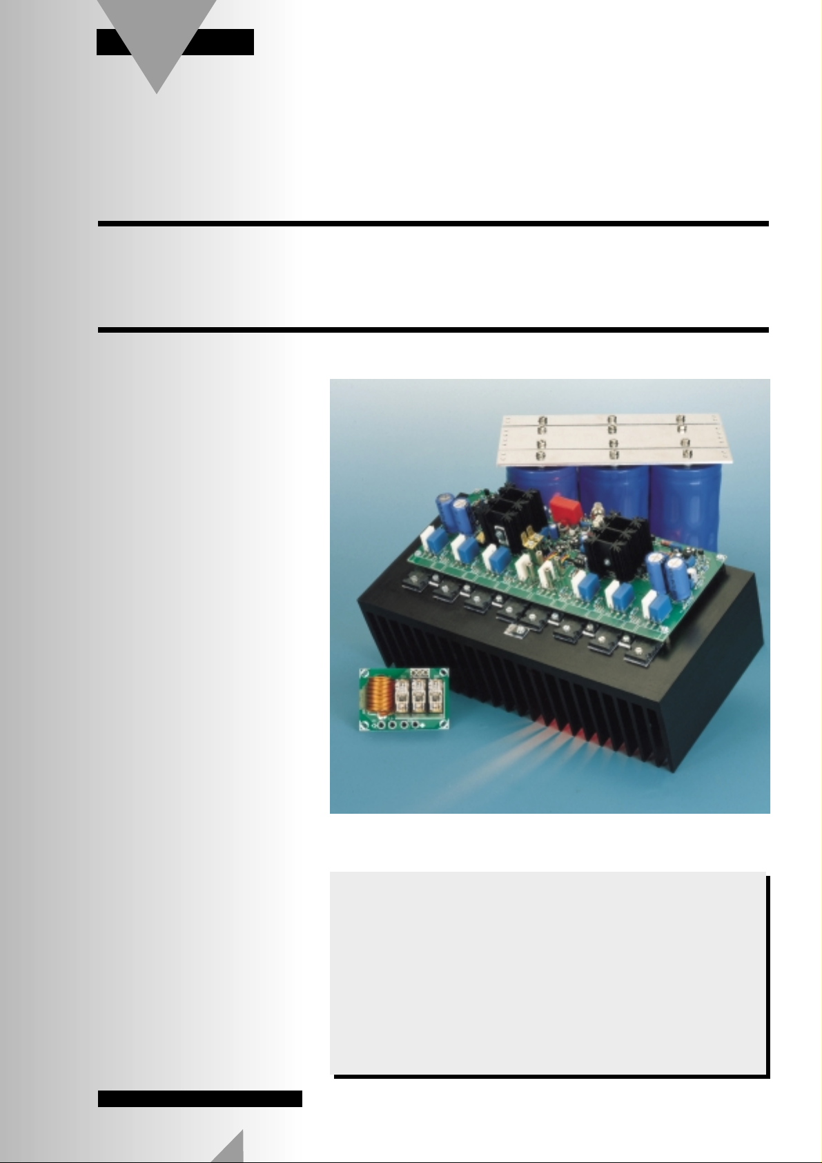
Elektor Electronics 2/99
It could be argued
that most of the out-
put amplifiers pub-
lished in this maga-
zine lack power.
Although this is a
debatable point, it
was felt that a true
heavyweight output
amplifier would make
a welcome change for
many constructors.
The Titan 2000 can
produce 300 watts
into 8 Ω, 500 watts
into 4 Ω, and
800 watts into 2 Ω.
For those who believe
that music power is a
reputable quantity, the
amplifier can deliver
2000 watts of this
magical power into
4 Ω.
58
Design by T. Giesberts
Titan 2000
High-power hi-fi and
public-address amplifier
Brief parameters
Sine-wave power output 300 W into 8 Ω; 500 W into 4 Ω; 800 W into 2 Ω
Music power* 2000 W into 4 Ω
Harmonic distortion <0.005%
Slew limiting 85 V µs
–1
Open-loop bandwidth 55 kHz
Power bandwidth 1.5 Hz – 220 kHz
*See text about the validity of this meaningless quantity.
AUDIO & HI-FI
Contents
Page 2
INTRODUCTION
Amplifier output has been a cause of
argument for as long as there have
been audio power amplifiers. For
domestic use, a power rating of
2× 50 W is more than sufficient. With
the volume control at maximum and
the use of correctly matched goodquality loudspeakers, this will provide
a sound pressure level (SPL) equivalent to that of a grand piano being
played forte in the same room.
However, not all amplifiers are
intended for domestic use: many are
destined for discos, small music halls
and other large rooms. But even here,
what power is really required? Since
doubling the amplifier output increases
the SPL by a barely audible 3 dB, it was
felt that 300 watts sine wave power into
8Ωwould appeal to many .
‘ PROGRAMMABLE’
POWER OUTPUT
The amplifier has been designed in
such a manner that its output is ‘programmable’ as it were. With a sine
wave input, it delivers an average
power of 300 W into an 8Ω load,
which should meet the requirements
of all but the power drunk. Compared
with the output of 50 W from a
domestic audio amplifier, this
gives an increase in SPL of
7.5 dB. If even higher outputs are
needed, the load impedance may be
lowered to 4 Ω, which will give an
increase in SPL of 10 dB compared
with a 50 W output.
Although music power is a deprecatory term, since it does not really
give the true power rating of an amplifier, readers may note that the Titan
2000 can deliver 2 kW of this magical
power into 4 Ω. (True power is average
power , that is, the product of the r.m.s. volt-
age across the loudspeaker and the r.m.s.
current flowing into the speaker. The term
music power is generally meaningless,
because to some manufacturers it means the
product of the peak voltage and peak current; to others it means merely double the
true power; and to yet others, even more
disreputable, it means quadrupling the true
power).
However, power is not the only criterion of an amplifier. Low distortion,
good slew limiting, and an extended
power bandwidth, as possessed by the
Titan 2000, are also hallmarks of a good
amplifier.
Power bandwidth denotes the frequency range over which the power
falls to not less than half its maximum
value. This is much more telling than
the frequency response, which is usually measured at a much lower output
level.
Slew limiting is the maximum input
voltage change that can occur in one
59
Elektor Electronics 2/99
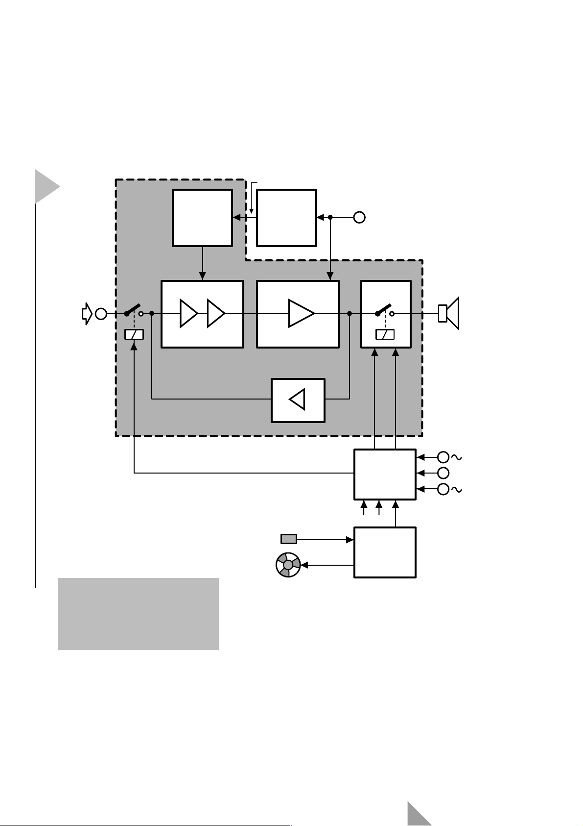
1
Figure 1. Simplified block diagram of the Titan 2000. The auxiliary power supply, protection
networks and thermal control
are discrete circuits built on discrete PCBs.
Contents
regulator
± 78V
T43...T52
voltage amplifier
T1...T10
T15...T26
input stages &
cascode amplifiers
± 85V
auxiliary
power supply
2x 15V
current amplifier
T27...T34
T35...T42
drivers & output stages
offset control
main power
supply
± 70V
heat sink
sensor
fan
protection
circuits
UinU
thermal
control
out
990001 - 12
0
Page 3
60
Elektor Electronics 2/99
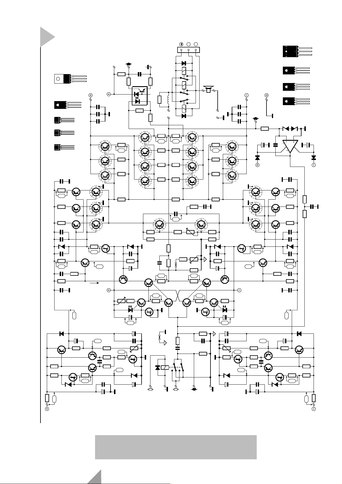
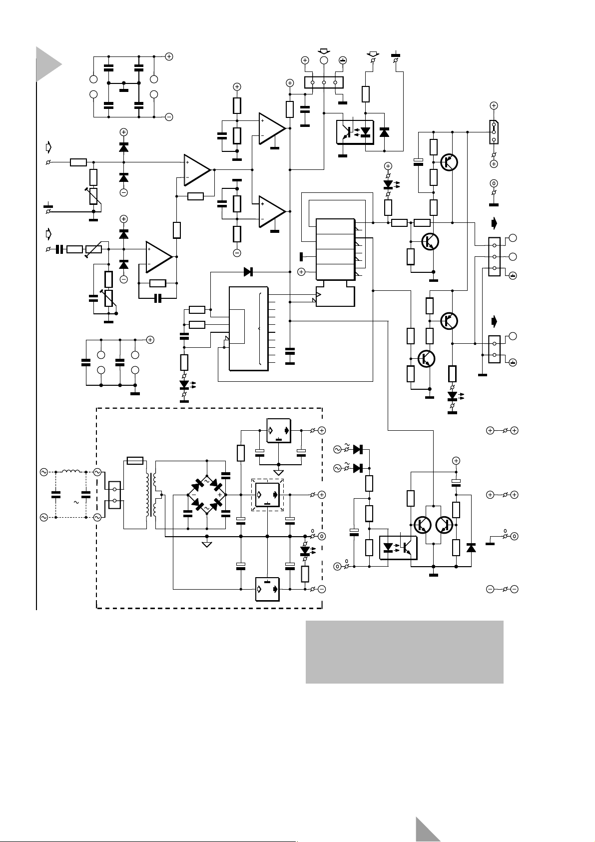
Figure 2. Although the circuit diagram gives the impression of a highly complex design, the amplifier is, in
essence, fairly straightforward.
2
Contents
R56
85V
BF871
BD711
BC550
BF245A BC639
R62
R57
15Ω
BF872
BD712
BC560
BC640
BF256C
R26
R25
R24
D4
R18
R13
T47
330Ω
15k
1V
2R
1R
K1
2SC5359
1M
C24
2µ2 63V
1N4004
T24...T26=MJE340
R17
-39V
T51
2x
15n
T50
D11
220n
100V
470µ
2SA1987
2SC5171
MJE340
BD139
1µ
150Ω
R72
BC
640
T48
30V
2SA1930
MJE350
BD140
D14
2
5
7
1
C19
T18 T19 T20
C23
C22
D6
C11
R20
C5
R15
C18
-78V
C39
15k
BF
245A
1W3
0W5
12V
3
IC1
6
68Ω
0V83 0V83
68Ω
68Ω
270Ω
1V45 1V45
1k00
2µ2
63V
R67
I
+5V
2k2
C42
R78
C
EB
5V
C45
100n
C44
100n
C43
100n
T31
T30
BE
E
B
C
BE
C
S
GD
70V
C
T29...T31=2SC5171
T21...T23=MJE340
3k3
R22
T11
2mA1
63V
T46
BC
639
T45
R58
270Ω
0V36
T29
T23
T22
T21
1W
T13
53V-53V
15V
39V
12k
R64
22Ω
R61
C31
15n
22Ω
R60
C29
220n
C28
470µ 100V
C17
100p
68Ω
T17
68Ω
T16
68Ω
T15
C21
100p
C20
100p
5V6
0W5
C8
100n
270Ω
150Ω
R16
C4
2n2
1k00
C16
100p
+78V
D10
1N4004
C32
2µ2
BD712
15k
R63
2x
BF
245A
T43
D8
30V
1W3
R76
10Ω
R41
38mV32mV
10Ω
R40
10Ω
R39
560Ω
R36
BF256C
D5
R19
T9
P2
250Ω
D1
8V4
5k6
R59
39V
1n
R77
100Ω
6
8
IC2
2
T35...T38=2SC5359
C9
10k
C10
BF871
R5
330Ω
C6
1V71V7
C34
C33
P4
T44
BF256A
D9
C30
100Ω
5
7
6N136
3
2Ω2
R79
100Ω
R74
33Ω
R75
0Ω22
25V
100V
1W3
63V
R48
0Ω22
R47
0Ω22
R46
0Ω22
R45
BD
139
T27
220Ω
R33
22k
R31
1n
C3
T3
5k
22Ω
R12
53mV53mV
22Ω
R4
T7
BF
245A
JP2
D3
1N4148
T38
T37
T36
T35
15V
1W3
100n
1W
100µ
T5
220µ
25V
470µ
220n
39V
47µ
MUTE
D18D19
L1
Re4 Re3 Re2
LS+ LS+
0Ω22
R52
20mV20mV
0Ω22
R51
0Ω22
R50
0Ω22
R49
150Ω
R38
R30RC14
C15
100n
2V24
R34
500Ω
470Ω
P3
470Ω
R11
470Ω
JP1
R10
45mV45mV
T1
R2
C1
Re1
390Ω
R9
T2
562Ω
2µ2
5k
P1
22Ω1
R8
22Ω
R14
R6
V23042-A2003-B101
LS1
T39...T42=2SA1987
T39 T40 T41 T42
C
T28
T4
22Ω
T6
T8
BF
245A
47k
R3
C2
1n
1M
R1
P-IN
T27...T42 on common heatsink
LS- LS-
10Ω
R44
10Ω
R43
10Ω
R42
560Ω
R37
BD
140
220Ω
R35
22k
R32
15V
1W3
D7
C12
100n
10k
1W
R21
C13
25V
100µ
T10
470Ω
R7
C7
C41
C40
P5
5k6
R68
39V
D12
C37
220µ
D2
25V
470µ
220n
47µ
C48
C47
C46
BF872
100V
5k
BF256A
1W3
63V
100n
100n
100n
T32 T33 T34
T14
15V
-30V
T49
-39V
70V
P-LS
R53
C26
D16
T32...T34=2SA1930
15V
T24 T25 T26
1W
BF256C
3k3
R23
35V 35V
T12
12k
R73
22Ω
R70
C38
22Ω
R69
C36
C35
D15
4
100p
R29
R28
R27
100p
100p
5V6
100n
2n2
100p
D13
BD711
270Ω
0V36
E
C
B
990001 - 11
E
C
B
B
C
E
B
C
E
C27
2µ2 63V
OP90G
D17
1N4004
15V
4M7
R54
C25
68n
4M7
R55
0W5
T1, T4, T5, T15...T17 = BC560C
T2, T3, T6, T18...T20 = BC550C
1N4004
T52
330Ω
R71
15k
R66
1V
15Ω
R65
85V
Page 4
microsecond, and to which the amplifier can respond.
DESIGN
CONSIDERATIONS
The Titan 2000 is based on the ‘compact power amplifier’ published in the
May 1997 issue of this magazine. That
was a typical domestic amplifier with a
power output of 50 W into 8 Ω or 85 W
into 4 Ω. The special property of this
fully balanced design was the use of
current feedback instead of voltage
feedback, which resulted in a fastresponding amplifier with a large
open-loop bandwidth. The amplifier
performed well both as regards instrument test and measurements and listening tests. However, to serve as a
basis for the Titan 2000, its output current and drive voltage range had to be
increased substantially.
For a start, the supply voltage has to
be more than doubled, which means
that transistors with a higher power
rating have to be used in the power
supply . The higher supply voltage also
results in larger potential drops across a
number of components, and this
means that dissipation problems may
arise.
The large output current required
for the Titan 2000 makes a complete
redesign of the current amplifier used
in the ‘compact power amplifier’
unavoidable, since that uses insulatedgate bipolar transistors (IGBTs).
Although these are excellent devices,
the large spread of their gate-emitter
voltage makes their use in parallel net-
works next to impossible. To obtain the
requisite output power, the use of parallel networks of symmetrical pairs of
transistors is inevitable.
In view of the foregoing, bipolar
transistors are used in the current
amplifier of the Titan 2000. However,
these cannot be driven as readily as
IGBTs, which means that current drive
instead of voltage drive is used. This
entails a substantial upgrading of the
driver stages and the preceding cascode amplifiers (which also consist of a
couple of parallel-connected transistors). The good news is that the power
transistors in the Titan 2000 are considerably less expensive than IGBTs: an
important factor when eight of these
devices are used.
Finally, the protection circuits have
been enhanced in view of the higher
voltages and currents. The circuits protecting against direct voltages and
short-circuits are supplemented by
networks protecting against overload
and (too) high temperatures. The latter
is coupled to a proportional fan control.
In short, a large part of the Titan
2000 is a virtually new design rather
than a modified one.
BRIEF DESCRIPTION
The block diagram of the Titan 2000 is
shown in Figure 1. The voltage amplifier consists of input stages T
1–T10
, and
cascode amplifiers/pre-drivers T
15–T26
.
The current amplifier is formed by driver transistors T
27–T34
, and output
transistors T35–T42.
The offset control stage prevents
any direct voltage appearing at the
output of the amplifier.
The loudspeaker is linked to the
amplifier by three heavy-duty relays.
The current amplifier operates from
a ±70 V supply, which is provided by
two 50 V mains transformers. To enable
the voltage amplifier to drive the current amplifier to its full extent, it needs
a slightly higher supply voltage to
compensate for the inevitable losses
caused by inevitable voltage drops.
This is accomplished by superimposing
a ±15 V potential from an external
auxiliary supply on to the main ±70 V
supply and dropping the resulting
voltage to ±78 V with the aid of regulator T
43–T52
.
The combined protection circuits
constantly compare the input and output voltage of the amplifier: any deviation from the nominal values leads to
the output relays disconnecting the
loudspeaker and the input relay
decoupling the input signal.
The thermal protection circuit monitors the temperature of the heat sink
and, if necessary, switches on a fan. If,
with the fan operating, the temperature approaches the maximum permissible limit, the output relays are
deenergized and disconnect the loudspeaker.
CIRCUIT DESCRIPTION
The circuit diagram of the Titan 2000 is
shown in Figure 2. In spite of the large
number of components, the basic cir-
61
Elektor Electronics 2/99
Contents
Page 5
cuit is straightforward.
As already noted in
the previous paragraph, transistors
T
1–T10
form the input
amplifier, T
11
and T12are buffers, T
13
and T14are current sources, T15–T
26
form the cascode amplifier/pre-driver
stage, T
27–T34
are the driver transistors
in the current amplifier , T
35–T42
are the
output transistors, and T
43–T52
form a
sophisticated supply voltage regulator.
Input amplifier
Strictly speaking, the input amplifier is
formed by transistors T
3–T4
. Cascode
stages T
9–T10
serve merely to enable
the input section handling the high
voltages. These voltages are limited by
zener diodes D
5
and D7, which are part
of the potential divider that also sets
the operating points of T
21–T26
. In
view of the requisite stability, the current through the zener diodes is held
constant by current sources T
13
and
T
14
. Resistors R22and R23limit the
potential across, and thus the dissipation in, these field-effect transistors.
Otherwise, the input section is virtually identical to that of the ‘compact
power amplifier’. The drop across the
emitter resistors of buffers T
1
and T
2
determines the drop across the emitter
resistors of T
3
and T4, and consequently the setting of the operating
point of the overall input section. To
eliminate the influence of temperature
variations, T
1
is thermally coupled to
T
3
and T2to T4.
Since the operating point of buffers
T
1
and T2is critical, current sources T
5
and T6have been added. The reference
for these current sources is provided
by light-emitting diodes (LEDs) D
1
and
D
2
. The current through these diodes
is determined by current sources T
7
and T8. In view of the
requisite stability,
diode D
1
is thermally
coupled to T
5
and D
2
to T6.
Any imbalance of the input stages is
compensated by making the current
through T
5
equal to that through T
6
with potentiometer P2.
Cascode amplifiers/pre-drivers
The large output current of the Titan
2000 necessitates a proportionally
large pre-drive voltage, which is provided by three parallel-connected cascode amplifiers, T
15–T26
. The current
through these amplifiers is arranged at
10–15 mA, but the current feedback
used may cause this level to be appreciably higher. This is the reason that the
transistors used in the T
21–T26
positions are types that can handle currents of up to 50 mA when their collector-emitter voltage is 150V.
The input section is linked to the
cascode amplifiers by buffers T
11
and
T
12
, which results in a lowering of the
input impedance. The arrangement
also enables an increase in the values
of R
13
and R15, which results in a 3 dB
increase in amplification of the input
section.
The function of resistors R
19
and
R
21
is threefold: they limit the dissipation of the buffers; they obviate the
need of an additional voltage to set the
operating point of the buffers; they
limit the maximum current through
the buffers, and thus the cascode
amplifiers, to a safe value.
The open-loop amplification of the
Titan 2000 is determined solely by
those of the input section and cascode
amplifiers. The amplification of the
input section depends on the ratios
R
13
:(R12+R8) and R15:(R14+R8) and,
with values as specified is ×10 (i.e., a
gain of 20 dB).
The amplification of the cascode
amplifiers is determined largely by the
ratio of parallel-connected resistors R
31
and R32and the parallel network of
R
24–R26
. With values as specified, the
amplification is about ×850 (remem-
ber, this is a push-pull design), so that
the overall amplification of input section plus cascode amplifiers is ×8500 (a
gain of close to 80 dB).
Current amplifier
Since one of the design requirements is
that the amplifier is to work with loads
down to 1.5 Ω, the output stages consist of four parallel-connected pairs of
transistors, T
35–T38
and T39–T42. These
transistors have a highly linear transfer
characteristic and provide a direct-current amplification that remains virtually constant for currents up to 7 A.
Like the output transistors, the driver stages need to remain within their
safe operating area (SOA), which
necessitates a threefold parallel network. The transistors used in the driver stages are fast types
(f
T
=200 MHz).
Setting the bias voltage for the requisite quiescent current is accomplished by balanced transistors T
27
and
T
28
. These transistors are mounted on
the same heat sink as the output transistors and driver transistors to ensure
good thermal coupling and current
control. Of course, the current rises
during full drive conditions, but drops
again to its nominal level when the
amplifier cools off. The quiescent current is set to 200 mA with potentiometer P
3
.
Owing to the large output current,
the connection between amplifier output and loudspeaker is not arranged
via a single relay, but via three. Two of
these, Re
3
–Re4, are controlled in synchrony by the protection circuits.
When they are deenergized, their disabling action is delayed slightly to give
the contacts of the third relay , Re
2
, time
to open, which is of importance in a
fault situation.
Input relay Re
1
is switched off in
synchrony with Re
2
to ensure that
there is no input signal by the time Re
3
and Re4are deenergized.
Optoisolator IC
2
serves as sensor for
the current protection circuits. The
light-emitting diode in it monitors the
voltage across R
48–R52
via potential
divider R
74–R75
, so that the positive as
well as the negative output currents
are guarded. The use of an optoisolator prevents earth loops and obviates
compensation of the ±70 V commonmode voltage. The +5 V supply for the
optoisolator is derived from the protection circuits.
Feedback
The feedback loop runs from the out-
62
Elektor Electronics 2/99
3
Figure 3. Circuit diagram of the requisite
auxiliary power supply.
Contents
K1
12V / 1VA5
70V
Tr1
D3
D4
4x 1N4007
K2
D1
C3
100n
160mA T
R1
1M
D2
C1
470µ
100V
K3
F1
85V
70V
4x 1N4007
Tr2
D5
D6
12V / 1VA5
C4
100n
R2
1M
K4
F2
160mA T
990001 - 13
C2
470µ
100V
D7
D8
85V
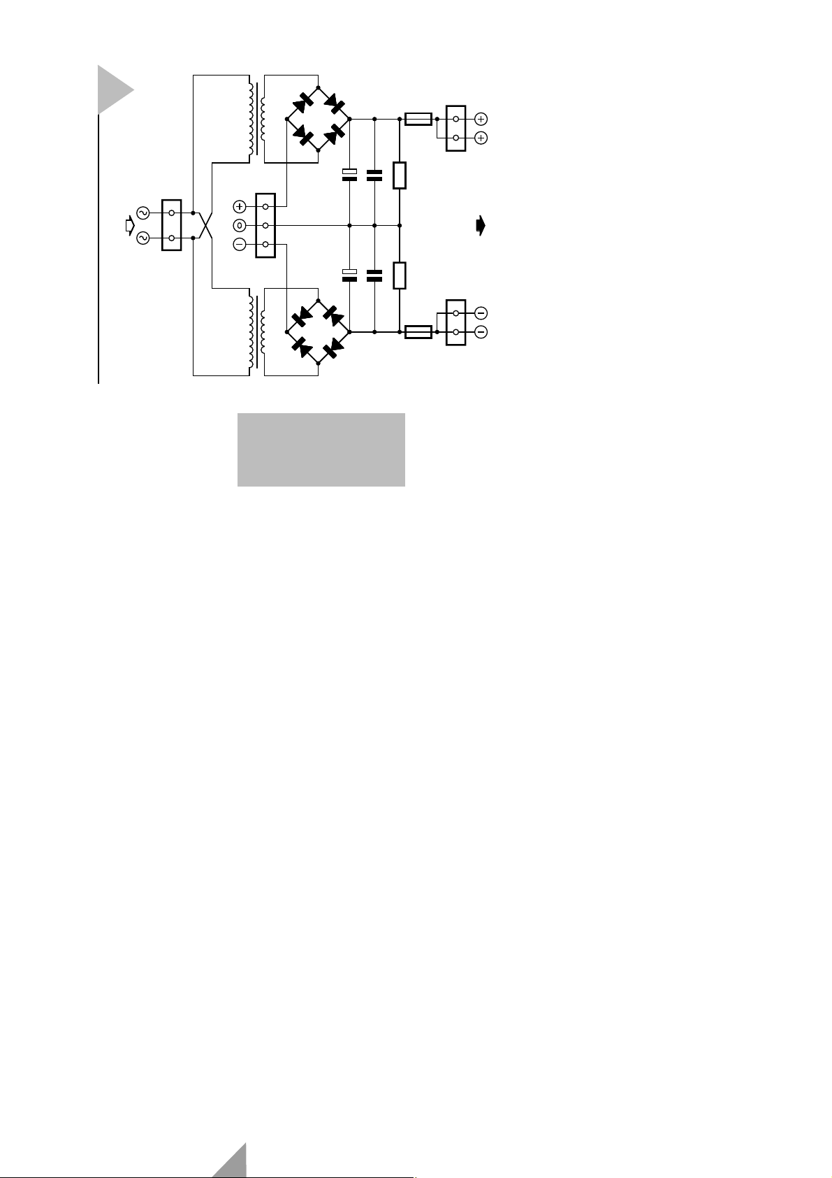
Page 6
put of the power stages to the junction
of T
3
and T4via resistors R10and R11.
This is current feedback because the
current through T
3
and T4depends on
the potential across R
8
, which is determined largely by the current through
R
10
and R11. The overall voltage amplification of the output amplifier is determined by the ratio R
8
:(R10+R11).
Compensation
Capacitors C3–C5and resistors R16, R
17
form part of the compensation network required for stable operation.
Low-pass filter R
2–C2
at the input is
essential to prevent fast, that is, highfrequency, signals causing distortion.
This filter is also indispensable for stability’s sake.
Coupling capacitor C
1
is needed
because the available offset compensation network merely redresses the bias
current of the input buffers and is not
intended to block any direct voltages at
the input.
Relay Re
1
at the input enables the
input signal to be ‘switched off’. It
forms part of the overall protection
and in particular safeguards the input
section against overdrive. The overall
protection circuit will be discussed in
detail next month.
Network R
9-P1
is intended specifically for adjusting the common-mode
suppression when two amplifiers are
used in a bridge arrangement. It is
needed for only one of these amplifiers, and may be interconnected or
disabled by jumper JP
1
as needed.
Offset compensation is provided by
integrator IC
1
, which ensures that if
there is any direct voltage at the output
of the amplifier, the operating point of
T
1-T2
is is shifted as needed to keep the
output at earth potential. The operational amplifier (op amp) used draws
only a tiny current (20 µA) and has a
very small input offset (450 µV).
Supply voltage for IC
1
is taken from
the ±15 V line for the input section via
diodes D
16
and D17. This arrangement
ensures that the supply to the IC is
retained for a short while after the
main supply is switched off so that any
interference is smoothed out.
Diodes D
14
and D15safeguard the
input of IC
1
against (too) high input
voltages in fault conditions.
The values of resistors R
54
and R
55
arrange the level of the compensating
current at not more than 1 µA, which is
sufficient to nullify the difference
between the base currents of T
1
and T2.
Regulation
Although current feedback has many
advantages, it also has a serious drawback: poor supply voltage suppression.
This makes it essential for the supply
voltage for the voltage amplifier to be
regulated. In view of the requisite high
symmetrical potential and the fact that
the unregulated voltage that serves as
input voltage can vary substantially
under the influence of the amplifier
load, two discrete low-drop regulators,
T
43–T47
and T48–T52are used.
As mentioned before, owing to
inevitable losses through potential
drops, the supply voltage for the input
section and cascode amplifiers needs to
be higher than the main ±70 V line.
Furthermore, the input voltage to the
regulators must be higher than the
wanted output voltage to ensure effective regulation.
Fortunately, the current drawn by
the voltage amplifier is fairly low
(about 70 mA) so that the input voltage
to the regulators can be increased with
a simple auxiliary supply as shown in
Figure 3. This consists of two small
mains transformers,two bridge rectifiers, D
1–D4
and D5–D8, and the neces-
sary reservoir and buffer capacitors.
The ±15 V output is linked in series
with the ±70 V line to give an unregulated voltage of ±85 V.
The 39 V reference is provided by
zener diode D
9
. This means that the
regulator needs to amplify the reference voltage ×2 to obtain the requisite
output voltage.
The zener diode is powered by cur-
rent source T
43
, to ensure a stable reference, which is additionally buffered
by C
30
.
Differential amplifier T
45-T46
, whose
operating point is set by current source
T
44
, compares the output voltage with
the reference via potential divider
R
63-R64-P4
. This shows that the output
voltage level can be set with P
4
.
Transistor T
47
is the output stage of
the regulator. The output voltage
remains stable down to 0.2 V below the
input voltage.
63
Elektor Electronics 2/99
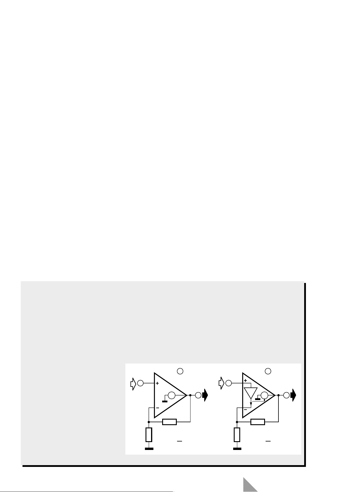
Current-feedback
In an amplifier using voltage feedback (Figure a), the differential voltage at its inputs is multiplied by the open-loop
amplification. The feedback loop forces the output voltage to a level that, divided by network R
1-R2
, is equal to the
input voltage.
Whereas an amplifier with voltage feedback has high-impedance inputs, an amplifier with current feedback (Figure
b) has an high-impedance and a low-impedance input. Its input stage consists of a buffer with unitary gain between
the inverting and non-inverting inputs. Essentially, the inverting input is the low-impedance input. The buffer is followed by an impedance matching stage that converts the output current of the buffer into a directly proportional output voltage.
The current feedback loop operates as follows. When the potential at the non-inverting input rises, the inverting input
will also rise, resulting in the buffer current flowing through resistor R
1
. This current, magnified by the impedance
matching stage, will cause the output
voltage of the amplifier to rise until the
output current flowing through resistor R
2
is equal to the buffer current through R1.
The correct quiescent output voltage can
be sustained by a very small buffer current. The closed-loop amplification of the
circuit is determined by the ratio
(1+R
2
):R1.
A interesting property of an amplifier
with current feedback is that the closedloop bandwidth is all but independent of
the closed-loop amplification, whereas
that of an amplifier with voltage feedback
becomes smaller in inverse proportion to
the closed-loop amplification – a relation
known as the gain-bandwidth product.
Contents
U
in
A(s)
ab
U
out
U
in
R2
R1
R2
A
= 1 +
v
R1
R1
R(s)
A
=1
v
I
R2
A
= 1 +
v
R2
R1
990001 - 14
U
out
Page 7
65
Elektor Electronics 2/99
Resistor R57and diode D8protect T
43
against high voltage during switch-on,
while D
10
prevents current flowing
through the regulator in the wrong
direction.
Capacitors C
31
and C32enhance the
rate of operation of the regulator.
Network R
56-C28-C29
provides
additional smoothing and r.f. decoupling of the ±85 V lines.
NEXT MONTH
Next month’s second and concluding
instalment of this article will describe
details of the protection circuits, the fan
control, and the construction of the
amplifier. The instalment will also
include detailed specifications and performance characteristics.
[990001-1]
Contents
Page 8
Elektor Electronics 3/99
SIX FUNCTIONS
The integrated protection network consists of six sub-circuits:
• power-on delay
• transformer voltage sensor
• temperature sensor
• current sensor
• direct-current sensor
• overdrive sensor
The power-on delay ensures that the
relays in the amplifier are energized
50–100 milliseconds after the supply
has been switched on to prevent
switch-on clicks.
The transformer voltage sensor
reacts to the cessation of the secondary
voltage of the mains transformers to
prevent switch-off clicks and crackles.
The temperature sensor responds to
excessive heat sink temperatures, but it
should be noted that this works only in
This second of four
parts deals primarily
with the protection
network incorporated
in the amplifier. This
indispensable net-
work safeguards the
amplifier and the
loudspeakers con-
nected to it against all
kinds of error that
may arise. The net-
work is an indepen-
dent entity with its
own power supply.
32
Design by T. Giesberts
Titan 2000
Part 2: protection network
INTRODUCTION
As mentioned briefly in Part 1, extensive and thorough protection is a must
in an amplifier of this nature. It may
well be asked why this is so: is there
such a likelihood of mishaps arising?
Or is the amplifier so vulnerable? On
the contrary: extended tests on the
prototype have shown that the Titan
2000 is a very stable and reliable piece
of equipment. In fact, unusual means
had to be used to actuate the protection circuits during these tests, since
not any standard test prompted the
amplifier into an error situation.
The extensive protection is necessary because by far the largest number
of mishaps occur owing to actions by
the user, not because of any shortcomings in the amplifier. For example, the
most robust and reliable amplifier can
not always cope with extremely high
overdrive or overload conditions.
Correction. In last month’s first part
of this article, it was stated erroneously that the article consists of
two parts, whereas in fact it will be
described in four parts.
AUDIO & HI-FI
Contents
Page 9
conjunction with the fan drive, which
is reverted to later in this article.
The current sensor monitors the
output current, while the direct-current and overdrive sensors form a
combined circuit that monitors differences between the input and output
signals, and reacts to excessive directcurrent levels or distortion. This circuit
is the most important and ‘intelligent’,
but also the most complex of the six.
All sensors, when actuated, react in
the same way: they cause the output
relays and the mute relay at the input
of the amplifier to be deenergized
immediately. This action causes the
input signal and the
output load to be disconnected from the
amplifier. After the fault
causing the sensor
action has been
removed or remedied, the relevant
protection circuit is disabled, whereupon the amplifier relays are reenergized after a short delay.
When the protection network is
actuated, a red LED lights to indicate
an error. When the fault has been
removed or remedied, the red LED
remains on, but a yellow LED flashes
to indicate that the amplifier will be
reenabled shortly. The red LED then
goes out, shortly followed by the yellow, whereupon a green LED lights to
indicate that all is well.
COMMON SECTION
AND POWER
- ON DELAY
The circuit of the integrated protection
network, including the +5 V and ±12 V
power supplies, is shown in Figure 4.
33
Elektor Electronics 3/99
V
V
4
Figure 4. The protection network consists of six sensor circuits each of which
causes the input and output relays of
the amplifier to be deenergized when a
fault occurs.
Contents
LSP
input
C1
100n
R1
R5
680Ω
30µH
2x 100n
250V
100k
IC1
P2
C2
C16
100n
8
4
500Ω
R2
1k05
1n
16
IC3
P1
250Ω
8
C12
100n
C13
100n
R6
820k
K4
P3
500k
12V
12V
12V
12V
C17
100n
C14
100n
C15
100n
D1
2x
BAT82
D2
D3
2x
BAS45A
D4
16
IC4
8
F1
50mA T
Tr1
3
2
5V
2x 15V
8VA
IC2
IC1a
R7
11
6
1M
12V
12V
C3
100n
IC1 = OP249GP
IC2 = LM319
5
IC1b
6
R4
10k0
R3
10k0
1
R14
2M2
R13
470k
C7
470n
R15
1k
D6
EARLY
B80C1500
C26
47n
temp
I
11
12
13
IC2a
IC2b
3
4
5
6
7
8
9
5V
R12
C6
2k2
100n
12
3
7
8
4
5
12
13
5V
7
5
4
6
14
13
15
1
2
3
C8
100n
9
1
12V
R8
47k
4
R9
C4
100n
7
C5
100n
11
10
9
12
12V
RCX
RX
CX
CT=0
IC3
470Ω
R10
470Ω
R11
47k
CTR14
!G
D5
+
5
9
10
1N4148
CT
74HC4060
IC4
74HC175
1D
C1
R
5
4
K1
IC5
4N35
R16
4k7
126
D7
R19
47k
R24
47k
47k
R25
R20
2M7
C9
4µ7
63V
R23
4k7
2k2
R22
R21
2k2
T1
BC
R27
4k7
4k7
R26
T3
BC
547B
547B
T2
T4
R28
BD
140
BD
140
3k9
D9
ON
1N
4148
5V
D8
ERROR
R17
1k
2
3
7
6
10
11
15
14
R18
47k
Vre
12V
JP1
Vre Ext.
K2
K3
int
ext
2R
1R
mute
IC9
12V
+5V
5V
+5V
+12
+12V
4µ7
C18
4µ7
63V
C19
4µ7
63V
C22
63V
+12V
+5V
D13
R35
3k3
+5V
+12V
POWER
50V
50V
D10
D11
C10
10µ
63V
2x
1N4007
R32
15k
R31
15k
R30
3k3
IC6
126
4N35
R29
47k
5
4
5V
C11
47µ 25V
BC
547B
R34
T6
100k
R33
D12
100k
1N4001
T5
2x
7805
R36
C23
22Ω
47µ
C20
1000µ
25V
C21
470µ
25V
25V
IC7
7812
IC8
C24
47n
B1
C25
47n
7912
–12V
–12V
–12V
12V
–12
990001 - 2 - 11
Page 10
The network is linked to the input
and output of the amplifier via terminals ‘input’ and ‘LSP ’ respectively (to
terminals ‘P-IN’ and ‘P-LS’ on the
amplifier board).
Terminals ‘50 V≈’ are connected to
the secondary windings of the mains
transformers.
The three output relays and the
mute relay in the amplifier are linked
to the protection network via K
2
, and
K
3
respectively.
The current sensor is connected to
the output of optoisolator IC
2
in the
amplifier (‘I->’ on the amplifier board)
via K
1
.
The terminals marked ‘temp’ are
intended to be linked to the output of
the fan control circuit.
As mentioned earlier, the action of
each sensor results in the deenergizing
of the output and mute relays in the
amplifiers. This implies that the outputs of the the various sensor circuits
are interlinked. This is effected by combining the open-collector outputs of
these circuits into a wired OR gate with
R
12
functioning as the common pullup resistance. The combined output
signal serves to reset a number of
34
Elektor Electronics 3/99
-12V
~
~
Parts lists
Protection network
Resistors:
R
1
, R33, R34= 100 kΩ
R
2
= 1.05 kΩ
R
3
, R4= 10.0 kΩ
R
5
= 680 Ω
R
6
= 820 kΩ
R
7
= 1 MΩ
R
8
, R11, R18, R19, R24, R25, R29= 47 kΩ
R
9
, R10= 470 Ω
R
12
, R21, R22= 2.2 kΩ
R
13
= 470 kΩ
R
14
= 2.2 MΩ
R
15
, R17= 1 kΩ
R
16
, R23, R26, R27= 4.7 kΩ
R
20
= 2.7 MΩ
R
28
= 3.9 kΩ
R
30
, R35= 3.3 kΩ
R
31
, R32= 15 kΩ
R
36
= 22 Ω
P
1
= 250 Ω, multiturn preset (upright)
P
2
= 500 Ω, multitun preset (upright)
P
3
= 500 kΩ, multiturn preset (upright)
Capacitors:
C
1
, C3= 0.1 µF
C
2
= 0.001 µF
C
4
, C5, C6, C8, C12–C17=0.1 µF,
ceramic
C
7
= 0.47 µF
C
9
, C18, C19, C22= 4.7 µF, 63 V, radial
C
10
= 10 µF, 63 V, radial
C
11
, C23= 47 µF, 25 V, radial
C
20
= 1000 µF, 25 V, radial
C
21
= 470 µF, 25 V, radial
C24–C26= 0.047 µF, ceramic
Semiconductors:
D
1
, D2= BAT82
D
3
, D4= BAS45A
D
5
, D7= 1N4148
D
6
, D8, D9, D13= 3 mm high-efficiency
LED
(yellow, red, green, green respectively)
D10, D11= 1N4007
D
12
= 1N4001
T
1
, T3, T5, T6= BC547B
T
2
, T4= BD140
Integrated circuits:
IC
1
= OP249GP (Analog Devices)
IC
2
= LM319N
IC
3
= 74HC4060
IC
4
= 74HC175
IC
5
, IC6= 4N35
IC
7
= 7812
IC
8
= 7912
IC
9
= 7805
Miscellaneous:
JP
1
= 2.54 mm pin strip and pin jumper
K
1
, K2= 3-way terminal block, pitch
5mm
K3= 2-way terminal block, pitch 5 mm
K
4
= 2-way terminal block, pitch 7.5 mm
B
1
= bridge rectifier, rectangular, Type
B80C1500
F
1
= fuse, 50 mAT and fuse holder
Tr
1
= mains transformer, 15 VA, with
2×15 V secondary
Heat sink (for IC
7
) = e.g. Fischer
SK104, 50 mm
Mains interference filter
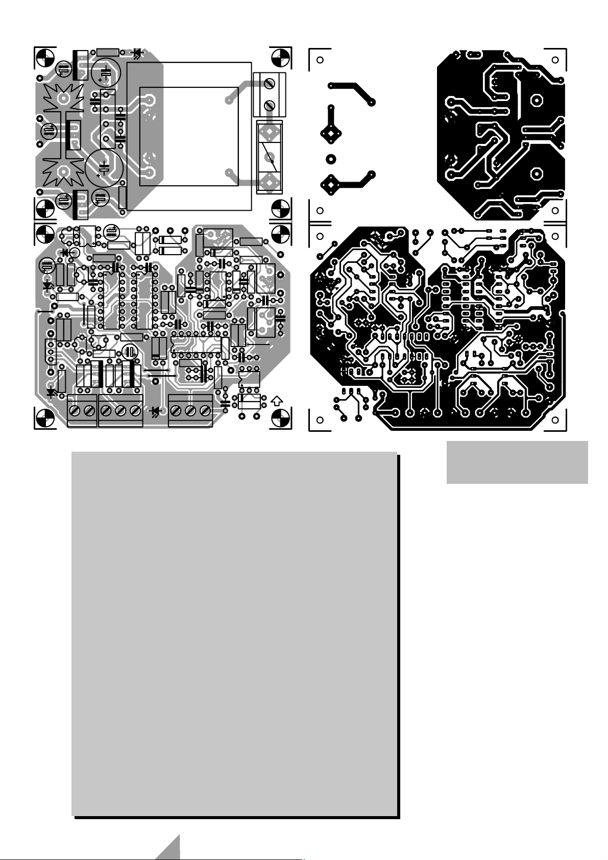
Figure 5. The printed-circuit
board of the overall protection network.
Contents
+12V
0
+5V
D8
+5V
0
Vre
ext
int
+12V
D9
H8
H7
H4
C11
H3
C18
T5
C19
C22
R34
R25
JP1
R28
mute
R17
R24
IC8
IC7
R33
T3
K3
T6
D12
R26
C8
C21
C20
IC6
R18
R27
IC9
C26
T4
R29
R21
R35
B1
R20
C23
IC4
T1
R30
R22
C25
C24
R36
C10
C17
T2
R19
R31
R23
C9
R32
IC3
D13
TR1
~
~
0
R2
D10
D11
C13
C16
D1
R4
R13
R14
C12
C7
C5
D5
R15
IC2
R8
C15
C14
0
T
K2
D6
2R
I
P1
D2
D4
IC1
C3
D3
R3
R10
R9
R11
R12
-12V
+
K1
IC5
R16
C6
T
R1
R6
R7
R5
D7
temp
K4
F1
C4
H5
50mAT
H6
H2
LSP
P3
T
input
C1 C2
P2
990001-2
990001-2
(C) ELEKTOR
H1
990001-2
(C) ELEKTOR
Page 11

D-type bistables (flipflops), contained in
IC
4
, which are interconnected to form a
shift register. Note that D-type bistables
are essential since these can be set and
reset in a defined manner.
The outputs of IC
4
are used to drive
two level converters, T
1-T2
and T3-T
4
respectively, which bridge the difference between the 5 V level of the logic
ICs and the 12 V supply for the relays.
Jumper JP
1
enables a different, external
supply voltage (V
RE
) to be used if 12 V
relays are not employed.
Transistors T
1
and T2drive Re1and
Re
2
, which are the first to be energized
(synchronously). On switch-off, capacitor C
9
ensures that T2remains on for
some milliseconds longer during
which period Re
3
and Re4are deener-
gized (see Part 1).
The power-on delay, which also
operates after a fault situation, is more
complex than usual. To start with, after
the supply voltage us switched on,
input CLR of IC
4
is held low (active)
for a few seconds by the circuit around
T
6
. When, after this period, CLR is
made high by R
12
–which happens
only when there is no error situation
(any longer)–the internal oscillator of
IC
3
is enabled via D5. This results after
a few seconds in a clock pulse appearing at the CLK input of IC
4
, where-
upon Q
4
goes high. The period
between the oscillator being enabled
and the appearance of
the first clock pulse is
not defined since,
owing to the presence
of T
6
, a power-on reset is purposely not
provided. To ensure a minimum delay
in the energizing of Re
1
and Re2in
spite of this, a high level is clocked into
Q
4
after IC3has been enabled. The precise moment at which this happens
varies, therefore, only when the supply
voltage is switched on for the first time.
A period of IC
3/Q3
later, Q1of IC
4
goes high, whereupon Re1and Re2are
energized. After another period, Q
2
of
IC
4
becomes high, whereupon Re3and
Re
4
are energized. At the same time,
IC
3
is disabled since its reset is inter-
linked with Q
2
of IC4.
The red LED, D
8
, in parallel with Q
1
of IC4lights when the relays in the
amplifier are not energized, either
because the amplifier is (not yet)
switched on, or owing to an error .
The yellow LED, D
6
, is linked to the
output of the oscillator in IC
3
, causing
it to flash until IC
4
is clocked.
The green LED, D
9
, is connected in
parallel with Re
3
and Re4, so that it
lights only when the amplifier is fully
switched on.
TRANSFORMER
VOLTAGE SENSOR
The 50 V≈ secondary voltages of the
mains transformers in the amplifier are
rectified by diodes D
10
and D11, and
smoothed by R30-R31-R32-C10. The values of these components ensure that
the LED in optoisolator IC
6
lights sufficiently to hold the associated photo
transistor on. This transistor pulls the
base of T
5
to ground, causing T5to cut
off. When the secondary voltages fail,
T
5
is switched on immediately via R29,
whereupon the D-type bistables in IC
4
are reset.
Use is made of an optoisolator purposely to avoid any risk of earth loops
between the supply return and the
ground of the protection network,
which is linked to the input ground of
the amplifier.
TEMPERATURE SENSOR
The temperature sensor works in a
manner similar to that of the transformer voltage sensor . The optoisolator
in this circuit is IC
5
, which, in contrast to
IC
6
, is normally cut off and comes on
only when the heat sink becomes
excessively hot.
The sensor reacts to the fan control
circuit switching the fan speed to maximum (because the heat sink is getting
too hot). A comparator in the fan control circuit then toggles, whereupon
IC
5
is actuated via the ‘temp’ input and
resets the D-type bistables in IC
4
. This
situation changes only after the heat
sink has cooled down to an acceptable
temperature (although the fans may
still be rotating).
CURRENT SENSOR
To nullify high common-mode voltages
and to prevent any risk of earth loops,
the current sensor also uses an optoisolator, IC
2
(Figure 5). However, this is
not located on the protection board,
but directly at the output of the amplifier.
The values of the relevant components cause the sensor to be actuated
when the output current is about 40 A.
This may appear a very large current,
but this is due entirely to the specified
requirement that the amplifier must be
capable of delivering 60 V into a load
of 1.5 Ω without the protection circuit
being actuated. The current level may
be lowered to some extent by increasing the value of R
74
in the amplifier.
Output resistor R
78
is in parallel
with R
12
by linking terminals ‘I’, ‘+5 V’
and ground on the amplifier board to
K
1
on the protection board via three
lengths of insulated, stranded circuit
wire twisted together. This arrange-
35
Elektor Electronics 3/99
Figure 6. Completed prototype of the protection
network.
Contents
Page 12
37
Elektor Electronics 3/99
ment ensures a low impedance to any
interference and a high reaction speed.
DIRECT- CURRENT AND
OVERDRIVE SENSOR
The d.c. and overdrive sensor constantly compares the input and output
signals of the amplifier and reacts
when the difference between the two
is too great. The comparison is effected
with the aid of operational amplifier
IC
1
which has a very low bias current
and a very low offset. It is, of course,
essential that during the comparison of
the two signals by differential amplifier
IC
1b
the differences in phase and transit times do not lead to error detection.
At the same time, the voltage amplification (×43) of the amplifier must be
taken into account.
The amplification is compensated
by potential divider R
1-R2-P1
at input
LSP. The potentiometer is a multiturn
type to ensure accurate adjustment.
The phase difference is compen-
sated by the circuit based on IC
1a
. The
transit at high and low cut-off points
is simulated by first-order networks
that can also be adjusted very accu-
rately with multiturn potentiometers P
2
and P3.
The inputs of IC
1a
and IC
1b
are protected by diodes. Since any
leakage current of these diodes, combined with the high input impedance
(≈ 1MΩ) of IC
1a
, might lead to an
appreciable offset, and therefore to an
unwanted error detection, the diodes,
D
3
and D4, are special types with a
leakage current of only 1 nA.
The output of differential amplifier
IC
1b
is monitored by a window com-
parator formed by IC
2a
and IC2b. The
value of the components used in
potential dividers R
8-R9
and R10-R
11
ensures that the protection circuit is
actuated when the direct voltage
reaches a level of ±5 V or the distortion
becomes 2.5 per cent. Such distortion
will normally be the result of overdrive, but the circuit reacts equally well
to oscillations or other spurious signals
that cause too large a difference to be
detected.
CONSTRUCTION AND
SETTING UP
The integrated protection network is
best built on the printed-circuit board
shown in Figure 5. Populating this
board should not present any undue
difficulties, but it should be noted that
diodes D
6
, D8, D9and D13, are not
located on the board, but are linked to
it via flexible, stranded circuit wire.
They are fitted to the front of the enclosure.
Jumper JP
1
will normally be in position ‘intern’ unless relays with a coil
voltage other than 12 V are used.
A prototype of the completed pro-
tection board is shown in Figure 6.
All input and output terminals of
the board are clearly marked with the
same symbols as shown in Figure 4.
Most interconnections can be made in
thin, stranded hook-up wire to
DEF61-12, but the input and output
links (‘input’ and ‘LSP’) must be
screened audio cable.
Although the power supply for the
protection network can be fitted on the
same board, the relevant section may
be cut off and fitted elsewhere. Of
course, the supply lines must then be
linked to the relevant terminals on the
protection board via insulated,
stranded hook-up wire.
The power supply is straightforward. From the secondary output of
the specified mains transformer, Tr
1
, a
symmetrical ±12 V supply is obtained
with the aid of regulators IC
7
and IC8.
From the same secondary, a +5 V supply for the digital circuits is obtained
with the aid of regulator IC
9
. Since the
relays are fed by the +12 V line, regulator IC
7
must be fitted on a heat sink.
To ensure that the protection network is not actuated by interference on
the mains supply , it is advisable to precede the power supply by a suitable
noise filter. This may be made from a
30 µH choke and two 0.1 µF, 300 V≈
capacitors as shown in dashed lines in
Figure 4.
The network is set up by maximizing the common-mode suppression
7
Parts lists
Auxiliary power supply
Resistors:
R
1
, R2= 1 MΩ
Capacitors:
C
1
, C2= 470 µF, 100 V, radial
C
3
, C4= 0.1 µF, 100 V, pitch 7.5 mm
Semiconductors:
D
1–D8
= 1N4007
Miscelleneous:
K
1
= 2-way terminal block, pitch 7.5
mm
K
2
= 3-way terminal block, pitch
7.5 mm
K
3
, K4= 2-way terminal block, pitch
5mm
Tr
1
, Tr2= mains transformer, 1.5 VA,
with 12 V secondart
F
1
, F2= fuse, 160 mAT, and fuse
holder
Figure 7. Printed-circuit board
for the auxiliary power supply
described in Part 1.
Contents
H1
990001-3
990001-3
(C) ELEKTOR
K1
~~
H2
(C) ELEKTOR
990001-3
TR1
TR2
H4
D1
D2
F1
0.16AT
C1
D3
D4
D5
D6
C2
F2
D7
D8
0.16AT
C3
+++
K2 K3K4 R1R2
C4
0
---
H3
Page 13
38
Elektor Electronics 3/99
9
with the aid of an oscilloscope or a
multimeter with sufficient bandwidth.
Measurements need to be made at
1 kHz, 20 kHz, and 20 Hz. The opencircuit amplifier is driven as far as possible by a suitable sine-wave generator
or CD player with a test CD.
With a signal of 1 kHz, set P
1
for
minimum sign al at the output of IC
1b
,
follow this with a signal of 20 kHz and
adjusting P
2
, and finally, with a signal
of 20 Hz, by adjusting P
3
. Since the settings influence one another to some
extent, the potentiometers should be
set a couple of times, perhaps also at
some different audio frequencies.
POWER SUPPLY
The auxiliary power supply described
in Part 1 is best constructed on the
printed-circuit board shown in Fig-
ure 7. The mains voltage is linked to
K
1
, the ±70 V to K2and the +85 V and
–85 V lines to K
3
and K4respectively.
Since all currents are low level, the
wiring may be made in thin, insulated,
stranded hook-up wire. A completed
prototype board is shown in Figure 8.
The main supply for the amplifier is
a straightforward, unregulated type,
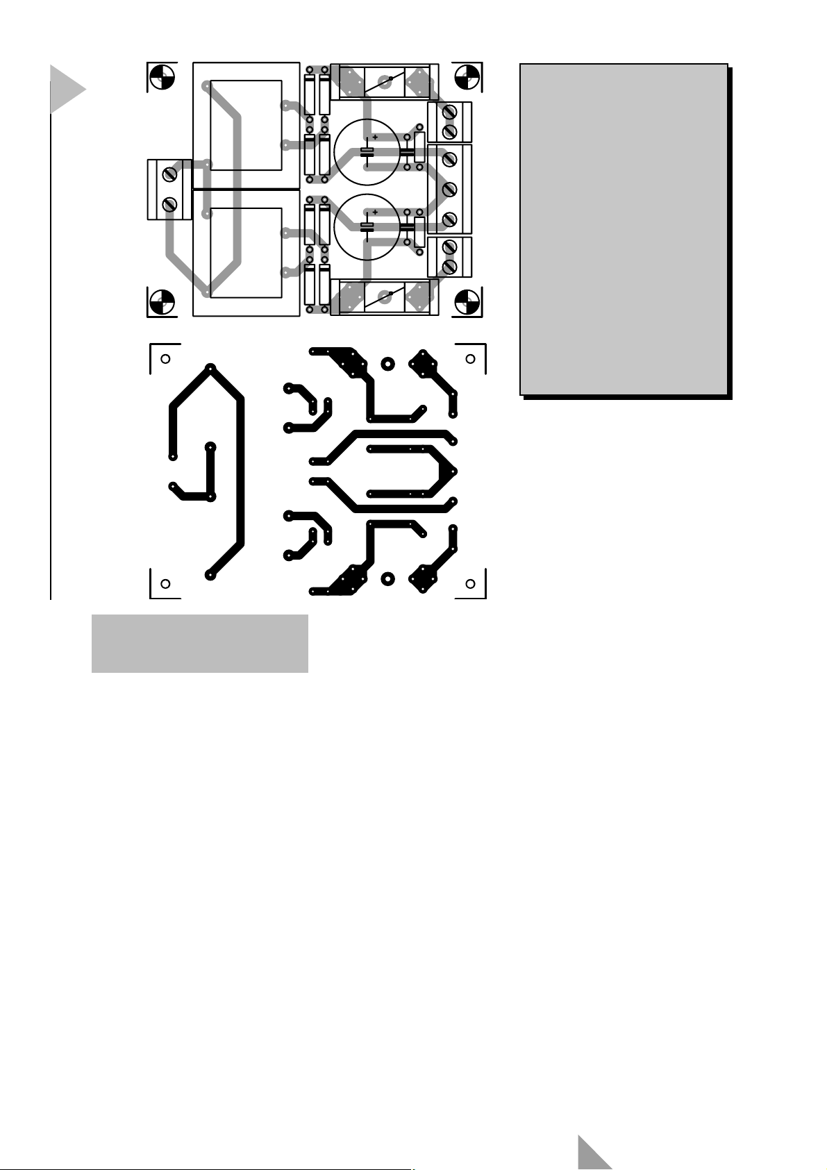
providing an output of ±70 V. Its circuit diagram is shown in Figure 9.
Since the specified requirements
call for a 2 Ω load, the supply must be
rated at 1000 VA, which necessitates
two toroidal transformers. To prevent
unforeseen equalizing currents, the
dual secondaries are not linked in parallel, but are individually connected to
a bridge rectifier. The outputs of the
rectifiers can be connected in parallel
without any problem. The rectifiers
need to be mounted on a suitable heat
sink such as a Type SK01.
It should be clear that the wiring of
the power supply must
allow for the large output currents of the
amplifier. In the prototype, the electrolytic
capacitors are linked by 3 mm thick
strips of aluminium. The remainder of
the wiring should be in insulated,
high-current wire to BS6231 with a
conductor size of 50/0.25 mm (2.5 mm
2
)
or better. The use of car-type connectors is recommended.
Note that the power supply as
described is intended for use with a
mono(phonic) amplifier that can deliver
800 W into 2 Ω and
should remain stable
with loads of 1.5 Ω. If
you are certain that you will always
use 4 Ω or 8 Ωloads, the power supply
requirements may be relaxed to some
extent. A reasonable relaxation is the
use of 2×50V/300 VA transformers and
10,000 µF/100 V smoothing capacitors.
The rating of the primary fuses may
then be reduced to 1.5 AT.
MAINS
- ON DELAY
The use of a mains-on delay is recommended when heavy loads are to be
switched on, as in the case of the present amplifier. Such a delay circuit
switches on the mains to the load gradually to ensure that the switch-on current remains within certain limits and to
prevent the mains fuses from blowing.
The most recently published (in this
magazine) mains-on delay is found in
the July/August 1997 issue (p. 74),
whose circuit diagram is reproduced in
Figure 10. Its printed-circuit board is
readily connected with the primary
windings of the two mains transformers. The board is not available readymade, however, and its diagram is,
therefore, reproduced in Figure 11.
8
Figure 8. The auxiliary
power supply is small
enough to fit in most
enclosures.
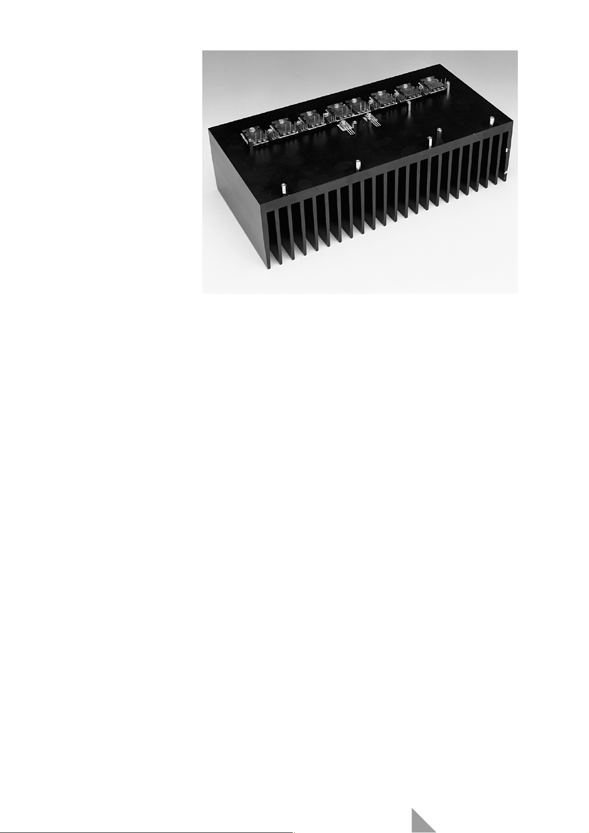
Figure 9. The main power supply for
the amplifier is a heavy-duty entity
in which the six capacitors are particularly impressive.
Contents
mains
power-on
delay
2A5 T
e.g. 974078 - 1
mains
power-on
delay
2x 50V
500VA
2x 50V
500VA
200V / 35A
200V / 35A
6x 22000µ / 100V
70V
1000VA
e.g. 974078 - 1
2A5 T
990001 - 2 - 12
70V
Page 14

39
Elektor Electronics 3/99
The delay arranges for the load,
that is, the Titan 2000, to be switched
on in two stages. In the first of these,
the switch-on current is limited by
series network R
4–R7
. After the delay
determined by capacitors C
2
and C3,
the series network is shorted by a relay
contact, whereupon the full current
flows between K
1
and K2.
Relay Re
1
can switch up to 2000 VA.
Its supply voltage is obtained from the
mains with the aid of rectifier B
1
,
capacitor C
1
and resistor R3.
Since the amplifier power supply
uses two mains transformers, two
mains-on delay circuits are needed.
Fuse F
1
functions as a primary
mains fuse for the amplifier.
Capacitor C
1
is a metallized paper
type intended especially for use with
mains voltage applications.
Bear in mind that the circuit is
linked directly to the mains supply and
thus carries lethal voltages.
Next month’s third instalment of
this article deals with the construction
of the amplifier, a few other practical
matters, and some measurements.
[990001-2]
Figure 10. The mains-on delay ensures that the
switch-on current remains within certain limit. Two of
these delays are required for each Titan 2000.
Figure 11. Printed-circuit board for the mains-on delay
circuit, which is not available ready made.
Parts lists
Mains-on delay circuit
Resistors:
R
1
, R2= 470 kΩ
R
3
= 220 Ω
R
4–R7
= 10 Ω, 5 W
Capacitors:
C
1
= 0.33 µF, 300 V a.c.
C
2
, C3= 470 µF, 40 V
Miscellaneous:
K
1
, K2= 2-way terminal block, pitch
7.5 mm
B1= bridge rectifier, round, Type
B250C1500
Re
1
= relay, coil 12 V, 1200Ω; contact
rating 250 V, 8 A
F
1
= see text
10
11
Contents
R1
K1
470kR2470k
C1
330n
*
250V
zie tekst
*
see text
*
voir texte
*
siehe Text
*
F1
R3
220Ω
*
~
B1
C3
470µ
40V
Re1
B250C1500
Re1 = V23057-B0006-A201
(250V / 8A)
C2
470µ
40V
R4
10Ω
5W
R5
10Ω
5W
R6
10Ω
5W
R7
10Ω
5W
K2
974078 - 11
~~~~
H3
F1
K1
R4
C1
R2
H4
974078-1
R1
R3
974078-1
B1
C3
R5
R6
RE1
H2
OUT
K2
R7
C2
H1
974078-1
Page 15

Elektor Electronics 4/99
INTRODUCTION
It is clear from the first two parts of this
article that the Titan 2000 is a complex
unit that needs to be constructed and
wired up with with great care to
ensure the specified performance. For
that reason, the construction notes will
be more detailed than is usual with
projects in this magazine. It is assumed
that the protection network and auxiliary power supply have already been
built and tested.
MOTHER BOARD
It must be borne in mind that in the
case of a fast power amplifier like the
Titan 2000, with a gain/bandwidth
product of about 0.5 GHz, the board
must be an integral part of the circuit.
The mother board is therefore
designed together with the remainder
of the circuit. The length of the tracks,
the area of the copper pads, the positions of the decoupling capacitors, and
other factors, are vital for the proper
and stable operation of the unit. Constructors who make their own boards
are therefore advised to adhere strictly
to the published layout.
Owing to the power requirements,
the various stages are parallel configurations. When these are mounted on
the heat sinks, a fairly large parasitic
capacitances to earth ensue. This is
because for reasons of stability all seven
heat sinks must be strapped to earth. It
This third of four parts
deals primarily with
the construction of the
amplifier and ends
with a brief resume of
its performance and
specifications. Let the
constructor beware,
however: the Titan
2000 is not an easy
project and certainly
not recommended for
beginners in elec-
tronic construction.
40
Design by T. Giesberts
Titan 2000
Part 3:
construction and setting up
AUDIO & HI-FI
Contents
Page 16

41
Elektor Electronics 4/99
T13 T14
Parts lists
It is regretted that, owing to circumstances beyond our control, component codings in the various sections
have been duplicated. Consequently,
the mother board, protection network
board, and auxiliary power supply
board contain many components
with the same identification (R
1-R36
,
C
1-C26
, D1-D12, T1-T6, IC1-IC2, JP1,
K
1
).
Amplifier
Resistors:
R
1
, R53= 1 MΩ
R
2
= 562 Ω
R3= 47 kΩ
R4, R6, R12, R14, R60, R61, R69, R70=
22 Ω
R5, R62, R71= 330 Ω
R7, R34= 470 Ω
R8= 22.1 Ω
R9= 390 Ω
R10, R11= 470 Ω, 5 W
R13, R15= 1.00 kΩ
R16, R17, R38= 150 Ω
R18, R20, R58, R67= 270 Ω
R19, R21= 10 kΩ, 1 W
R22, R23= 3.3 kΩ, 1 W
R24–R29= 68 Ω
R30= see text
R31, R32= 22 kΩ
R33, R35= 220 Ω
R36, R37= 560 Ω
R39–R44= 10 Ω
R45–R52= 0.22 Ω, inductance-free
R54, R55= 4.7 MΩ
R56, R65= 15 Ω
R57, R63, R66, R72= 15 kΩ
R59, R68= 5.6 kΩ
R64, R73= 12 kΩ
R74, R76, R77= 100 Ω
R75= 33 Ω
R78= 2.2 kΩ
R79= 2.2 Ω, 5 W
P1, P4, P5= 4.7 kΩ (5 kΩ) preset
P2= 250 Ω, preset
P3= 500 Ω, preset
Capacitors:
C1= 2.2 µF, metallized polyester
(MKP)
C2, C3, C42= 0.001 µF
C4, C5= 0.0022 µF
C6, C7= 220 µF, 25 V, radial
C8, C9, C11, C12, C15= 0.1 µF
C10, C13= 100 µF, 25 V, radial
C14= see text
C16–C23= 100 pF, 100 V
C24= 1 µF, metallized polypropylene
(MKT)
C25= 0.68 µF
C26, C27, C32, C39= 2.2 µF, 63 V,
radial
Figure 12. The double-sided printed-circuit board is intended to be combined with the
heat sink into a single entity. Before that can be done, however, the section for the output
relay and the inductor must be cut off the main section.
Contents
T
R79
T9
P4 P5
T10
H16
H15
H4
C8
R22 R23
H11 H12
D3
RE1
R1R2R3
P-IN
C11
H3
T49
T44
T
C10
LS+
C16
C9
mute
C18
R68
R59
C31
D4
D5
C25
R55
C2
D7
D6
C38
C32
R19
R54
R4
T1T2T3 T4
R6
C1
C13
C12
R21
C39
D11
D8
R58
R61
D2
R69
R70
R67
R60
1R
L1
K1
T
H14
D18D19
RE4
RE3
RE2
R13
LS-
C30
T43
D9
T45
R62
T47 T48
R63R64
C4
R18
R26
R16 R17
T11
C20
R57
T17
C33
T46
R25
C29
D10
T16
R24
C21
LS+
C17
T15
OUT2
T21T22T23
R56
990001-1
(C) ELEKTOR
C28
C34 C35
990001-1
H13
++
C43
C46
C44
R45
R49
H1
T35
T29
R39
T39
T32
R42
R46
-
R50
+
R47
R51
R48
R52
R38
R36
R40
R37
R43
R41
R44
T36
T30
T40
T37
T33
T41
T31
T38
T34
T42
H2
D16
P2
T7
R5
D1
T5
R12
P1
JP1
R14
T6
C7
R7
T8
C22
T12
C5
R15
R20
R29
R72R73
T52
T51
R71
D12
D17
P3
JP2
R27
C23
C19
R34
T18
C27
D15
IC1
D14
R53
LS+
C41
C42
+5V
R78
I
T27 T28
OUT1
P-LS
T
0 0
C47
H17H18
C45
R74
R75
C48
--
R77
R33
C15
R35
LS-
R11
T24T25T26
IC2
R76
R65
C26
C24
C6
R31 R32
R9
R8
C14
R30
C3
R10
T19
T20
R28
C40
D13
T50
C36
R66
C37
Page 17

42
Elektor Electronics 4/99
990001-1
Contents
(C) ELEKTOR
Page 18

is, of course, of paramount importance
that these capacitances are as small as
feasible. For this reason, it is vital that
in the thermal coupling of T
21–T34
1.5 mm thick ceramic—not mica—isolating washers are used. Mica washers
may , however, be used with the output
transistors since parasitic capacitances
there are of no significance.
The component and track layouts
of the mother board are shown in Fig-
ure 12. It will be seen that the board
consists of two sections: the mother
board proper and the output-relay
board. The latter must be cut off before
any other work is done. Later, when it
is built up, it is mounted on the mother
board with the aid of four 50 mm long
metal spacers in such a way that the
LS– and LS+ terminals on the two
boards are above each other. The spacers also provide the electrical link
between the boards.
The completed relay board is
shown in Figure 13. Inductor L
1
is
made from a doubled-up length of
1.5 mm enamelled copper wire wound
in two layers of eight turns each
around a 16 mm former (such as a
piece of PVC pipe). After the coil has
been wound, the PVC pipe is removed
and the four windings connected in
parallel. See Figure 14.
Ignoring the drivers and output
transistors for the moment, the construction of the mother board is traditional. As always, great care must be
taken during the soldering and placing
of components. Do not forget the thermal coupling of T
1-T3
, T2-T4, D1-T5,
D
2-T6
, T45-T46, and T50-T51, as already
pointed out in Part 1. Also, T
21–T23
and
T
24–T26
must be mounted on a heat
sink, and isolated from it by means of
a ceramic washer. When this is done, fit
the composite heat sinks on the board,
and link them to earth.
The input signal and the ±85 V
supply lines are linked to the board via
standard solder pins.
For connecting the ±70 V supply
lines and the relay board, 3 mm screw
holes are provided. Metal spacers are
to be fixed to these and cable connectors to the top of the spacers.
MAIN HEAT SINK
When the mother board has been completed, and carefully checked, as far as
described, it and the drivers and output transistors, T
27–T42
, must be
mounted on the main heat sink. This is
a 150 mm high Type SK157 from Fischer with a thermal resistance of
0.25 K W
–1
. This is admittedly a very
tedious job. It is vital that all requisite
fixing holes are drilled accurately in the
heat sink and preferably tapped with
3 mm thread. The template delivered
with the ready-made board is almost
indispensable for this work.
When the holes have been drilled
(and, possibly, tapped) transistors T
27
and T28should be fitted first (this is
important because they become inaccessible after the board has been fitted).
They must be located as close as possible to the output transistors and not in
the position indicated on the board.
Again, the template makes all this clear.
Their terminals must then be extended
with the aid of short lengths of equipment wire, which are later fed through
the relevant holes on the board and
soldered to the board via, for instance,
a three-way pin header.
The terminals of the drivers and
output transistors must be bent at right
angles: those of the former at the point
where they become thinner and those
of the latter about 5 mm from the body
of the device. When this is done, screw
all transistors loosely to the heat sink,
not forgetting the isolating washers. If it
is intended to use fan cooling, the requisite temperature sensor—that is, a
Type BD140 transistor— should also be
attached to the heat sink at this stage.
The template does not show a location
for the sensor, but it seems sensible to
fit it at the centre close to T
37
or T40.
The next step is to fit all ten spacers
to the heat sink: these should all be
10 mm long. In the prototype, spacers
with a 3 mm screwthread at one end
were used. Two of the spacers merely
provide additional support for the
relay board and another two form the
electrical link between the negative
supply line and the heat sink.
When all this work is done, the
board should look more or less like that
in Figure 15. Note that because of tests
later on, there are, as yet, no ceramic
isolating washers fitted on the prototype.
The next, and most tedious, step is
to combine the board and heat sink. It
is, of course, vital that all spacers are
exactly opposite the relevant fixing
holes and—even more tedious—that
the terminals of all transistors are
inserted into the correct mounting
holes. Bear in mind that the metal
43
Elektor Electronics 4/99
C28, C34, C35, C41= 470 µF, 100 V,
radial
C29, C33, C36, C40= 0.22 µF, 100 V
C30, C37= 47 µF, 63 V, radial
C31, C38= 0.015 µF
C43–C48= 0.1 µF, 630 V
Inductors:
L1= see text
Semiconductors:
D1, D2= LED, red, flat
D3, D18, D19= 1N4148
D4, D6= zener, 5.6 V, 500 mW
D5, D7= zener, 15 V, 1.3 W
D8, D11= zener, 30 V, 1.3 W
D9, D12= zener, 39 V, 1.3 W
D10, D13, D16, D17= 1N4004
D14, D15= zener, 12 V, 500 mW
T1, T4, T5, T15–T17= BC560C
T2, T3, T6, T18–T20= BC550C
T7, T8, T43, T48= BF245A
T9= BF871
T10= BF872
T11, T50, T51= BC640
T12, T45, T46= BC639
T13, T14= BF256C
T21–T23= MJE350
T24–T26= MJE340
T27= BD139
T28= BD140
T29–T31= 2SC5171 (Toshiba)
T32–T34= 2SA1930 (Toshiba)
T35–T38= 2SC5359 (Toshiba)
T39–T42= 2SA1987 (Toshiba)
T44, T49= BF256A
T47= BD712
T52= BD711
Integrated circuits:
IC1= OP90G
IC2= 6N136
Miscellaneous:
JP1, JP2= 2.54 mm, 2-way pinstrip
and pin jumper
K1= 3-way terminal block, pitch 5 mm
Re1= relay, 12 V, 600 Ω
Re2–Re4= relay, 12 V, 16 A, 270 Ω
Heat sink for T21–T26= 38.1 mm,
11 K W–1(Fischer Type SK104-STC;
TO220)
Heat sink for drivers/output transistors,
150 mm, 0.25 K W–1, Fischer Type
SK157
Ceramic isolation washers for T21–T34:
Fischer Type AOS220
Mica isolating washers for T35–T
42
PCB Order no 990001-1 (see Readers
Services towards end of this magazine)
Contents
Page 19
spacers for linking –, +,
LS+, and LS–, are
already on the board.
As the terminals of the
output transistors are
slightly longer than
those of the drivers, it may be possible
to do this work in two stages: output
transistors first and drivers second. It
may prove necessary to turn one or
more of the transistors slightly, which
is the reason that the fixing screws
have not yet been tightened. When all
terminals are correctly inserted, these
screws must, of course, be tightened
firmly.
The final step is to fix the relay
board on the spacers that form the link
for the LS– and LS+ terminals.
SETTING UP
Before the amplifier module can be
taken into use, presets P
2–P5
must be
set as required. Preset P
1
is intended
only for possibly adjusting the balance
in case of a bridge configuration.
Start by turning P
3
(the quiescentcurrent control) fully anticlockwise and
P
2
, P4, and P5, to their centre position.
Check the outputs of the power supply
and auxiliary power supply and, if
these are correct, link the +70 V line to
pins ‘+’ and ‘0’, the –70 V line to ‘–’
and ‘0’, the +85 V line to ‘++’ and the
-85 V line to ‘--’. For absolute safety, link
the ±70 V lines temporarily via a 10 Ω,
5 W resistor.
Next, set P
4
and P5for voltages of
+78 V and –78 V respectively at the
cases of transistors T
47
and T52respec-
44
Elektor Electronics 4/99
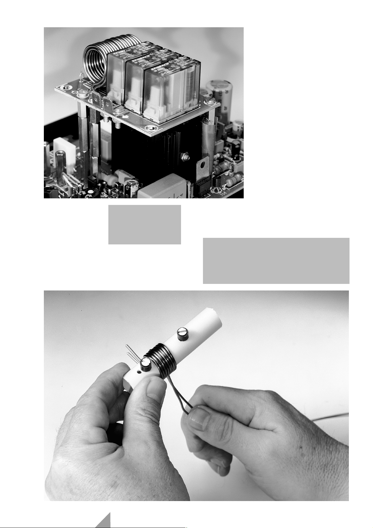
Figure 13. Illustrating
how the relay board is
mounted on the
mother board with the
aid of spacers.
Figure 14. Air-cored inductor L1is formed by laying two windings each of eight turns of doubledup each on top of one another. The former is a
length of 16 mm diameter PVC pipe as used by
plumbers. The resulting four windings are simply connected in parallel.
Contents
Page 20

tively (the cases of these transistors are
linked to the output of the relevant
regulator). It is important that the negative and positive voltages are numerically identical.
Since the parameters of the n-p-n
and p-n-p transistors in the input stage
are never exactly identical, there may
be a slight imbalance. This may be corrected by adjusting the output of current source T
5
with the aid of preset P
2
to give a potential of exactly 0 V at the
output (pin 6) of IC
1
(when ‘cold’).
Finally, insert an ammeter (set to
500 mA or 1 A range) in the +70 V or
–70 V line, and adjust P
3
carefully for a
quiescent current of 200 mA (cold condition—that is, immediately after
switch-on). With a large drive signal,
the quiescent current may increase to
some 600 mA, but at nominal temperatures, its level will stabilize at
200–400 mA. Note that these fluctuations have no noticeable effect on the
performance of the amplifier.
CHECK AND TEST
When the amplifier has been switched
on for about half an hour, the voltages
shown in Figure 2 (Part1) may be verified. Note that voltage levels depend-
ing on the setting of current sources
habitually show a substantial spread:
30 per cent is quite common. All measurements should be carried out with
a good digital voltmeter or multimeter
with a high-impedance input.
Other than the test voltages in the
circuit diagram, there are some others
that may be checked. For instance, the
proper functioning of the output transistors may be ascertained by measuring the voltage across R
45–R52
. Hold
one test probe against the loudspeaker
terminal and with the other measure
the potential at the emitters of all output transistors. The average value
should be about 20 mV, but deviations
of up to 50 per cent occur.
The voltage amplifier operation
may be checked by measuring its current drain: if this is within specification,
the voltage across R
56
and R65must be
within 0.8–1.1 V (after the amplifier has
been on for at least half an hour).
Finally, the potential drops across
the emitter resistors of differential
amplifiers T
45-T46
and T50-T51must not
differ by more than a factor 2. Too large
a factor is detrimental to the stable
operation of the amplifiers. A too large
difference may be corrected by chang-
ing the value of R62or R71, as the case
may be. If this is unsuccessful, the relevant transistor pair will have to be
replaced.
When all is well, the resistors in
series with the ±70 V lines should be
removed. Note that a rectified voltage
of 70 V, let alone one of 140V, is lethal. It
is therefore absolutely essential to
switch off the power supply and verify
that the residual voltages have
dropped to a safe value before doing
any work on the amplifier.
Next month’s instalment will deal
with the wiring up of the amplifier
and its performance, including specifications.
[990001-3]
45
Elektor Electronics 4/99
Figure 15. The PCB is
delivered with a template to ensure that
the transistors are fitted at the correct location on the heat sink.
Contents
101 48,5 0,5
22,7
T39 T40 T41T29 T30T32
300
T36 T42T35
T27
T37
T33
T28
T31
T38
T34
150
22,7 254,5
990001 - 3 - 13
Page 21

Elektor Electronics 6/99
BRIDGING:
PROS AND CONS
Bridging, a technique that became fashionable in the 1950s, is a way of connecting two single output amplifiers
(valve, transistor,
BJT, MOSFET, push-pull,
complementary) so that they together
control the passage of an alternating
current through the loudspeaker. This
article describes what is strictly a halfbridge configuration, a term not often
used in audio electronics. When audio
engineers speak of bridge mode, they
mean the full-bridge mode in which
four amplifiers are used.
In early transistor audio power
amplifiers, bridging was a means of
achieving what in the 1960s were called
public-address power levels as high as,
In the introduction to
Part 1 it was stated
that the Titan 2000
could deliver up to
2000 watts of ‘music
power’, a term for
which there is no stan-
dard definition but
which is still used in
emerging markets.
Moreover, without
elaboration, this state-
ment is rather misleading, since the reader will
by now have realized that the single amplifier
cannot possibly provide this power. That can
be attained only when two single Titan amplifiers are linked in a half-bridge circuit. The true
power, that is, the product of the r.m.s. voltage
across the loudspeaker and the r.m.s current
flowing into the loudspeaker, is then 1.6 kilo-
watts into a 4-ohm loudspeaker.
46
Design by T. Giesberts
Titan 2000
Part 5: half-bridging
two single amplifiers
GENERAL INTEREST
Contents
Page 22

say 50–80 W into 8 Ω.
Such power levels were
then way beyond of
what the voltage ratings of output transistors would permit.
Bridging is considered by many to
be a good thing, since it automatically
provides a balanced input (drive).
However, opponents will quickly point
out that it halves output damping,
doubles the circuitry and virtually cancels even-order harmonics created in
the amplifier.
Opponents also claim that bridging
amplifiers is tedious and requires too
much space. It is, however, not simple
either to design a single amplifier with
the same power output and the requisite power supply. A single 2 kW
amplifier requires a symmetrical supply voltage of ±130 V, that is, a total of
260 V. The power supply
for this would be quite a
design. And where
would a designer find
the drivers and output
transistors for this? Advocates point out that bridging amplifiers
have the advantage of requiring a relatively low supply voltage for fairly
high output powers.
Bridging just about doubles the
rated output power of the single
amplifier. Again, opponents point out
that loudness does not only depend on
47
Elektor Electronics 6/99
1
Figure 17. The interlinking required to form a half-bridge
amplifier from two single Titan 2000 units. Note that the
resulting balanced input may be reconverted to an unbalanced one with the Brangé design (Balanced/unbalanced
converters for audio signals) published in the March
1998 issue of this magazine. The PCB for that design
(Order no. 980026) is still stocked.
Contents
T35
T29
R39
R45
C43
T39
T32
R42
R49
C46
++
C28
C34 C35
R56
C29
T46
R57
C30
D9
T43
D8
R61
R58
C31
R59
T44
T49
R68
D11
R67
R70
D12
C37
R66
T50
C36
R65
--
C48
R52
990001-1
T15
C17
R24
T16
D10
R25
C33
T17
R26
R62
R18
T47 T48
T45
R60
C32
P4 P5
T11
C4
R16 R17
R63R64
R13
R19
D4
C16
C8
R22 R23
1
2
C11
C18
R71
R44
C41
T51
D13
R75
C39
R72R73
T52
R76
R78
IT+5V
R74
T34
D6
R21
R15
C5
R20
R29
C40
R28
R27
C19
R77
C42
R48
T38
C38
R69
T42
T21T22T23
C21
C20
T13 T14
3
D18D19
T12
T
T20
T19
T18
IC2
K1
1R
L1
C45
R41
T31
T36
T30
R36
R40
R46
C44
D14
D15
R53
C27
IC1
D17
C24
C26
P2
D16
D1
T7
R5
R4
D5
T9
T10
C12
C22
C23
R54
C25
C9
mute
C10
T
D7
C13
RE2
RE3
RE4
T24T25T26
R55
D3
RE1
C1
R6
D2
R7
T8
C7
LS+
C3
R10
R30
LS-
R11
*
LS+
C47
R51
R79
T41
R47
R37
R43
T33
T37
T40
R38
R50
T27 T28
C15
R33
R34
P3
R31 R32
C6
R12
T5
T3 T4
T1
R3
R1
T
P-IN
R2
T2
T6
R14
JP1
R9
R8
C14
R35
LS-
LS+
P-LS
+
T37
+
P-LS
LS+
LS-
R35
JP2
C14
R8
R9
JP1
R14
P1
T6
T2
R6
C2
R2
P-IN
T
R1
R3
R55
C2
T1
R4
T3 T4
T5
P1
R12
C6
R31 R32
C24
P3
R34
R33
C15
T27 T28
00
-
R50
R38
T40
-
00
JP2
T41
T33
R37
R43
R47
D2
R53
C47
LS+
R11
LS-
R10
R30
C3
LS+
C7
T8
R7
C1
RE1
D3
T
mute
C25
R54
R5
T7
D1
D16
P2
C26
D17
IC1
C27
D14
D15
T31
R79
T24T25T26
*
RE4
RE3
RE2
C13
C12
D7
T10
C10
C9
R41
R51
L1
C23
1R
K1
C22
T
D18D19
T13 T14
T9
D5
C20
C21
T21T22T23
T38
T34
R48
C45
T12
*
*
*
*
R74
R75
IT+5V
R78
C42
IC2
R76
R77
T18
C19
R27
T19
T20
R21
D13
R28
C40
R29
R20
T52
C5
R72R73
R15
C39
D6
C18
C11
JP2 niet plaatsen
do not use JP2
ne pas implanter JP2
JP2 nicht stecken
R22 R23
C8
C16
D4
R19
R13
R63R64
R16 R17
C4
T11
R18
R26
T17
C33
R25
T16
R24
T15
C17
990001-1
T42
R44
R52
C48
--
C41
R65
C36
T50
R66
R71
T51
R69
C38
P4 P5
C32
R60
T45
T47 T48
R62
D10
C34 C35
C37
D12
R70
R67
D11
R68
T49
T44
R59
C31
R58
R61
D8
T43
D9
C30
R57
T46
C29
R56
C28
++
C44
R46
R36
R40
T30
T36
R42
C46
R49
T32
T39
R39
T29
C43
R45
T35
990001 - 4 - 11
Page 23
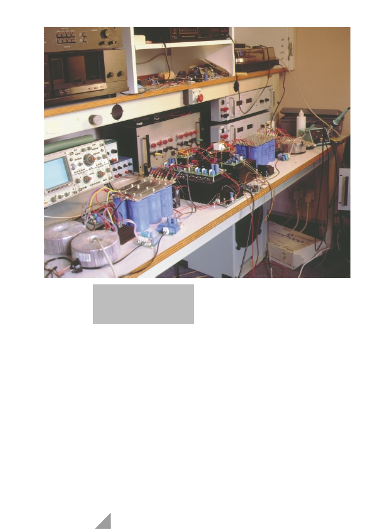
the amplifier, but
also on the loudspeaker. Bear in
mind, they say, that just changing a
loudspeaker with a sensitivity of, say,
90 dB
SPL
per watt per metre to one with
a sensitivity of 93 dB
SPL
per watt per
metre is equal to doubling the amplifier power rating.
Clearly , bridging two amplifiers is a
mixture of good and bad audio engineering and sonics.
INTERCONNECTING
It is, of course, necessary that two completed single Titan 2000 amplifiers are
available, each with its own power
supply. It should then be possible to
simply interlink the earths of the two
units, use the inputs as a common balanced input, and connect the loudspeaker between terminals LS+ on the
two amplifier. However, a few matters
must be seen to first.
Owing to the requisite stability , it is
imperative that the two amplifiers are
juxtaposed with the space between
them not exceeding 5 cm (2 in). They
should, of course, be housed in a com-
mon enclosure.
The inter-
wiring is shown
in Fig-ure 17. Make sure that the
power supplies are switched off and
that the smoothing capacitors have
been discharged before any work is
carried out.
Start by interlinking the negative
supply lines (terminals 0) with insulated 40/02 mm wire. Remove the
insulation at the centre of the length
of wire since this will become the central earthing point for the new (balanced) input. Link the ⊥ terminals on
both boards to the new central earth
with 24/02 mm insulated wire.
Connect the loudspeaker terminals
to the
LS+ terminals on the two boards
with 40/02 mm insulated wire.
Link pins 2 and 3 of the
XLR connec-
tor to the input terminals on the boards
with two-core screened cable. Solder
the screening braid to pin 1 of the
XLR
connector and to the new central
earthing point.
Finally, on both boards remove
jumper
JP
2
from the relevant pin strip.
FINALLY
When all interconnections between the
boards as outlined have been made,
the single amplifiers form a half-bridge
amplifier. If all work has been carried
out as described, there should be no
problems.
In the design stages, network R
9-P1
,
inserted into the circuit with pin
jumper
JP
1
(see Part1), was considered
necessary for common-mode suppression. However, during the testing of
the prototype, the network was found
to be superfluous. It may be retained if
the half-bridge amplifier is to be used
with a second half-bridge amplifier for
stereo purposes, when it may be used
to equalize the amplifications of the
two half-bridge amplifiers.
[990001]
48
Elektor Electronics 6/99
Figure 18. Test setup for the
prototype half-bridge amplifier
(centre). Note the large power
supplies at the left and right of
the amplifier.
Contents
Page 24
49
Elektor Electronics 6/99
Parameters
With a supply voltage of ±70 V (quiescent ±72 V) and a quiescent current of 200–400 mA
Input sensitivity 2.1 V r.m.s.
Input impedance 87 kΩ
True power output for 0.1%
THD 950 W into 8 Ω; 1.5 kW into 4 Ω
True power output for 1%
THD 1 kW into 8 Ω; 1.6 kW into 4Ω
Power bandwidth 1.5 Hz – 220 kHz
Slew limiting 170 V µs
–1
Signal+noise-to-noise ratio (at 1 W into 8 Ω) 97 dB (A-weighted
93 dB (B=22 kHz)
Total harmonic distortion (B=80 kHz)
at 1 kHz 0.0033% (1 W into 8 Ω)
0.002% (700 W into 8 Ω)
0.0047% (1 W into 4 Ω)
0.006% (700 W into 4 Ω)
at 20 kHz 0.015% (700 W into 8 Ω)
0.038% (1200 W into 4 Ω)
Intermodulation distortion
(50 Hz:7 kHz = 4:1) 0.0025% (1 W into 8 Ω)
0.0095% (500 W into 8 Ω)
0.004% (1 W into 4 Ω)
0.017% (500 W into 4 Ω)
Dynamic intermodulation distortion
(square wave of 3.15 kHz and 0.0038% (1 W into 8 Ω)
sine wave of 15 kHz) 0.0043% (700 W into 8 Ω)
0.005% (1 W into 4 Ω)
0.0076% (1200 W into 4 Ω)
Damping (with 8 Ω load) ≥ 350 (at 1 kHz)
≥ 150 (at 20 kHz)
Open-loop amplification ×8600
Open-loop bandwidth 53 kHz
Open-loop output impedance 3.2 Ω
A comparison of these parameters with the specifications given in Part 4 ((May 1999 issue) show that they are generally in line. In fact, the intermodulation distortion figures are slightly better. Because of this, no new curves are given
here other than power output (1 kW into 8 Ω and 1.6 kW into 4 Ω) vs frequency characteristics for 1 per cent total harmonic distortion.
During listening tests, it was not possible to judge the half-bridge amplifier at full volume, simply because there were
no loudspeakers available that can handle this power output. However, up to 200 W true power output, the half-bridge
amplifier sounds exactly the same as the single amplifier. Instrument test figures show no reason to think that the performance at higher output powers will be degraded.
Contents
4k
2k
1k
500
200
100
W
50
20
10
5
2
20 20k
50 100 200 500 1k 2k 5k 10k
Hz
990001 - 4 - 12
Page 25

33
Elektor Electronics 5/99
WIRING UP
How the various board, power supplies, controls and terminals are combined into an effective and interference-free unit is shown in Figure 16.
As already mentioned in Part 2, all
wiring carrying the main supply voltage (±70 V) must be insulated, highcurrent wire to BS6321 with a conductor size of 50/0.25 (2.5 mm
2
). This wire
should also be used to link the output
terminals of the power transistors and
the loudspeaker terminals. Any wiring
between smoothing capacitors and
the board should not exceed 15 cm
and be preferably much shorter. This
kind of wire is best terminated into
car-type connectors.
Other wiring may be made in
light-duty, stranded, insulated hookup wire. It is advisable (and may
prove to be very helpful in case of
problems) to use wire with different
colour insulation for dissimilar functions.
The connections between the input
socket and board must, of course, be
in screened audio cable. To avoid
earth loops, the socket should be isolated from a metal enclosure. Bear in
mind that the supply earth and the
enclosure are linked by metal spacers
between the two ‘0’ terminals and the
heat sink. It is, therefore, essential that
the heat sink is firmly strapped to the
metal enclosure.
This fourth of five parts deals primarily with the
wiring up of the amplifier and ends with a brief
resume of its performance and specifications.
The fifth and final part of the article in a forth-
coming issue will deal with the temperature
control, bridge configuration and some other
practical hints.
Design by T. Giesberts
Titan 2000
Part 4: wiring and performance
AUDIO & HI-FI
Contents
Page 26
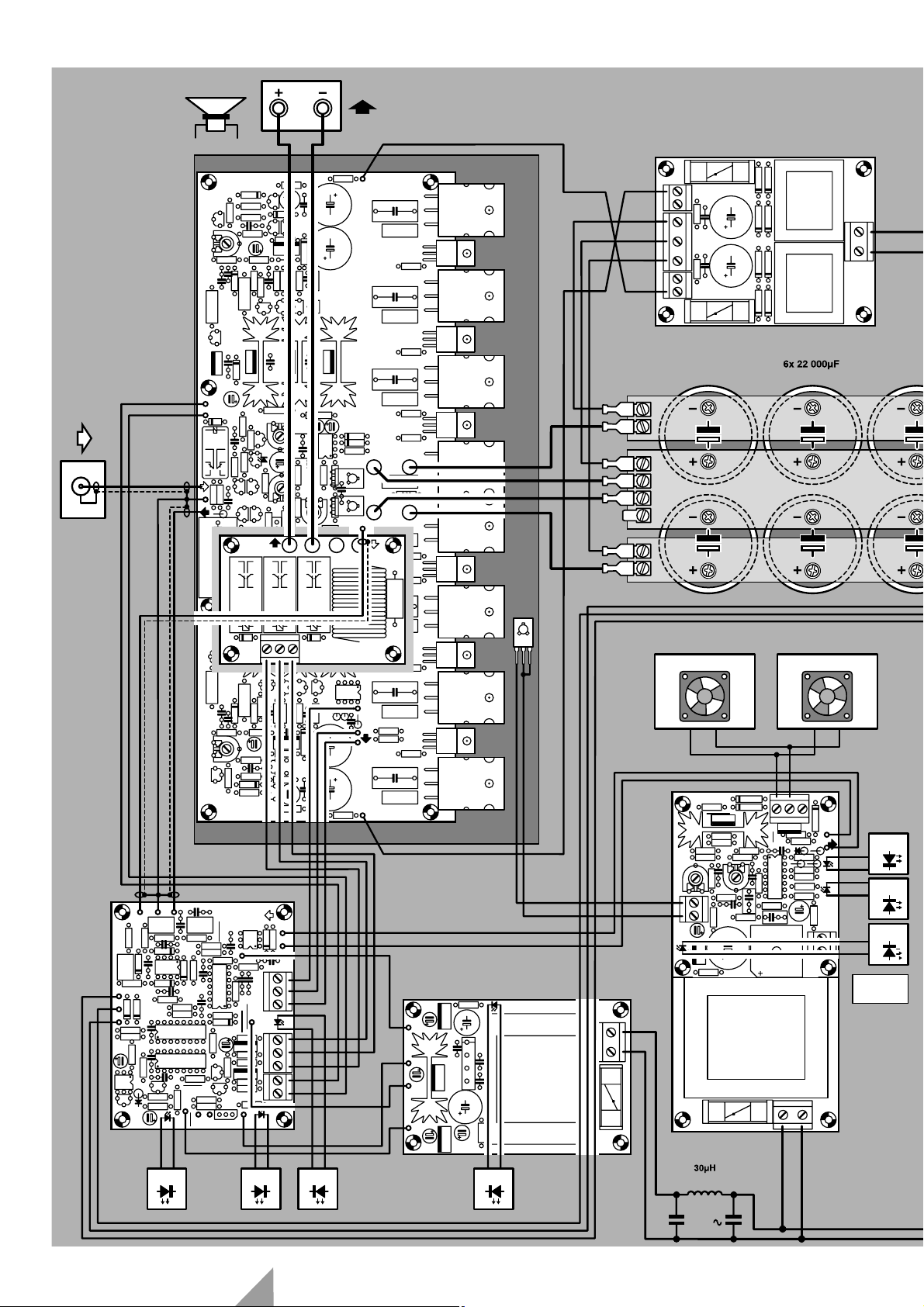
34
Elektor Electronics 5/99
C1
C2
C3
C4
C5
C6
C7
C8
C9
C10
C11
C12
C13
C14
C15
C16
C17
C18
C19
C20
C21
C22
C23
C24
C25
C26
C27
C28
C29
C30
C31
C32
C33
C34 C35
C36
C37
C38
C39
C40
C41
C42
C43
C44
C45
C46
C47
C48
D1
D2
D3
D4
D5
D6
D7
D8
D9
D10
D11
D12
D13
D14
D15
D16
D17
IC1
IC2
JP1
JP2
P1
P2
P3
P4 P5
R1R2R3
R4
R5
R6
R7
R8
R9
R10
R11
R12
R13
R14
R15
R16 R17
R18
R19
R20
R21
R22 R23
R24
R25
R26
R27
R28
R29
R30
R31 R32
R33
R34
R35
R36
R37
R38
R39
R40
R41
R42
R43
R44
R45
R46
R47
R48
R49
R50
R51
R52
R53
R54
R55
R56
R57
R58
R59
R60
R61
R62
R63R64
R65
R66
R67
R68
R69
R70
R71
R72R73
R74
R75
R76
R77
R78
RE1
T1T2T3 T4
T5
T6
T7
T8
T9
T10
T11
T12
T13 T14
T15
T16
T17
T18
T19
T20
T21T22T23
T24T25T26
T27 T28
T29
T30
T31
T32
T33
T34
T35
T36
T37
T38
T39
T40
T41
T42
T43
T44
T45
T46
T47 T48
T49
T50
T51
T52
--
++
+
-
00
LS+
LS-
I
T
+5V
mute
T
T
P-LS
P-IN
990001-1
B1
C18
C19
C20
C21
C22
C23
C24
C25
C26
D13
F1
IC7
IC8
IC9
K4
R35
R36
TR1
50mAT
-12V
+12V
0
+5V
~
~
C1 C2
C3
C4
C5
C6
C7
C8
C9
C10
C11
C12
C13
C14
C15
C16
C17
D1
D2
D3
D4
D5
D6
D7
D8
D9
D10
D11
D12
IC1
IC2
IC3
IC4
IC5
IC6
JP1
K1
K2
K3
P1
P2
P3
R1
R2
R3
R4
R5
R6
R7
R8
R9
R10
R11
R12
R13
R14
R15
R16
R17
R18
R19
R20
R21
R22
R23
R24
R25
R26
R27
R28
R29
R30
R31
R32
R33
R34
T1
T2
T3
T4
T5
T6
0
+12V
-12V
int
ext
Vre
0
0
~
~
LSP
input
T
+
I
T
+5V
temp
T
mute
2R
990001-2
B1
C1
C2
C3 C4
C5
C6
C7
C8
C9
D1
D2
D3
D4 D5
D6
D7
F1
IC1
IC2
K1
K2
K3
K4
P1
P2
R1
R2
R3
R4
R5
R6
R7
R8
R9
R10
R11
R12
R13
R14
R15
R16
R17
R18
R19
R20
R21
R22
R23
R24
R25
T1
T2
TR1
temp.
max.
T
T
~
~
63mAT
-
+
E
CB
12V
~
~
990041-1
C1
C2
C3
C4
D1
D2
D3
D4
D5
D6
D7
D8
F1
F2
K1
K2 K3K4 R1R2
TR1
TR2
990001-3
0
---
+++
~~
0.16AT
0.16AT
D18D19
K1
L1
R79
RE2
RE3
RE4
LS+
LS-
LS+
T
1R
ERROR ON EARLY
POWER
MAX.
ON
POWER
FAN
CONTROL
12V 12V
100V
BD140
TEMP.
SENSOR
2x 100n
250V
X2
Contents
Page 27

The on/off indicator, the functional
indicators, and the mains on/off
switch should, of course, be fitted on
the front panel of the enclosure. The
mains on/off switch must be a 10 A or
15 A type.
If the output power of the amplifier is limited to no more than 500 W,
in which case the enclosure does not
need fan cooling, the heat sink may
be mounted at the outside of the
enclosure or even form the sidewall
or back of a home-made enclosure.
For greater output powers, cooling
fans with relevant apertures at the
front and back of the enclosure are a
must. The heat sink must then be
located in the enclosure in such a
position that it is directly between the
two fans, ensuring a continuous supply of cooling air.
PERFORMANCE
The specification and associated comments in the box cannot, of course,
give a full impression of the performance of the amplifier. It is a wellknown fact that amplifiers with an
almost identical specification, and
using identical loudspeakers, can
sound quite different.
Particularly at low frequencies, the
amplifier maintains good control over
the loudspeaker, which results in a
clean fast (i.e., taut over the whole
audio range) sound, totally lacking in
reverberation. High and medium frequencies were also reproduced with
excellent definition and without any
trace of tizziness.
The overall impression is that the
amplifier has plenty of reserve and is
not strained in any circumstances.
In next month’s final instalment,
the temperature control and possible
bridge configuration will be discussed.
[990001-3]
35
Elektor Electronics 5/99
B1
C1
C2
C3
F1
K1
K2
R1
R2
R3
R4
R5
R6
R7
RE1
974078-1
~~~~
B1
C1
C2
C3
F1
K1
K2
R1
R2
R3
R4
R5
R6
R7
RE1
974078-1
~~~~
250V
10A
35A
200V
35A
200V
2x 50V
500VA
2x 50V
500VA
MAINS
F1 = 2A5 T F1 = 2A5 T
Figure 16. The wiring
diagram clearly illustrates how the various
parts of the amplifier
are combined into a
single unit.
Contents
ELEKTOR
50Hz240V
~
No. 990001
1000 VA
F = 2 x 2,5 A T
F = 63 mA T
F = 50 mA T
Page 28
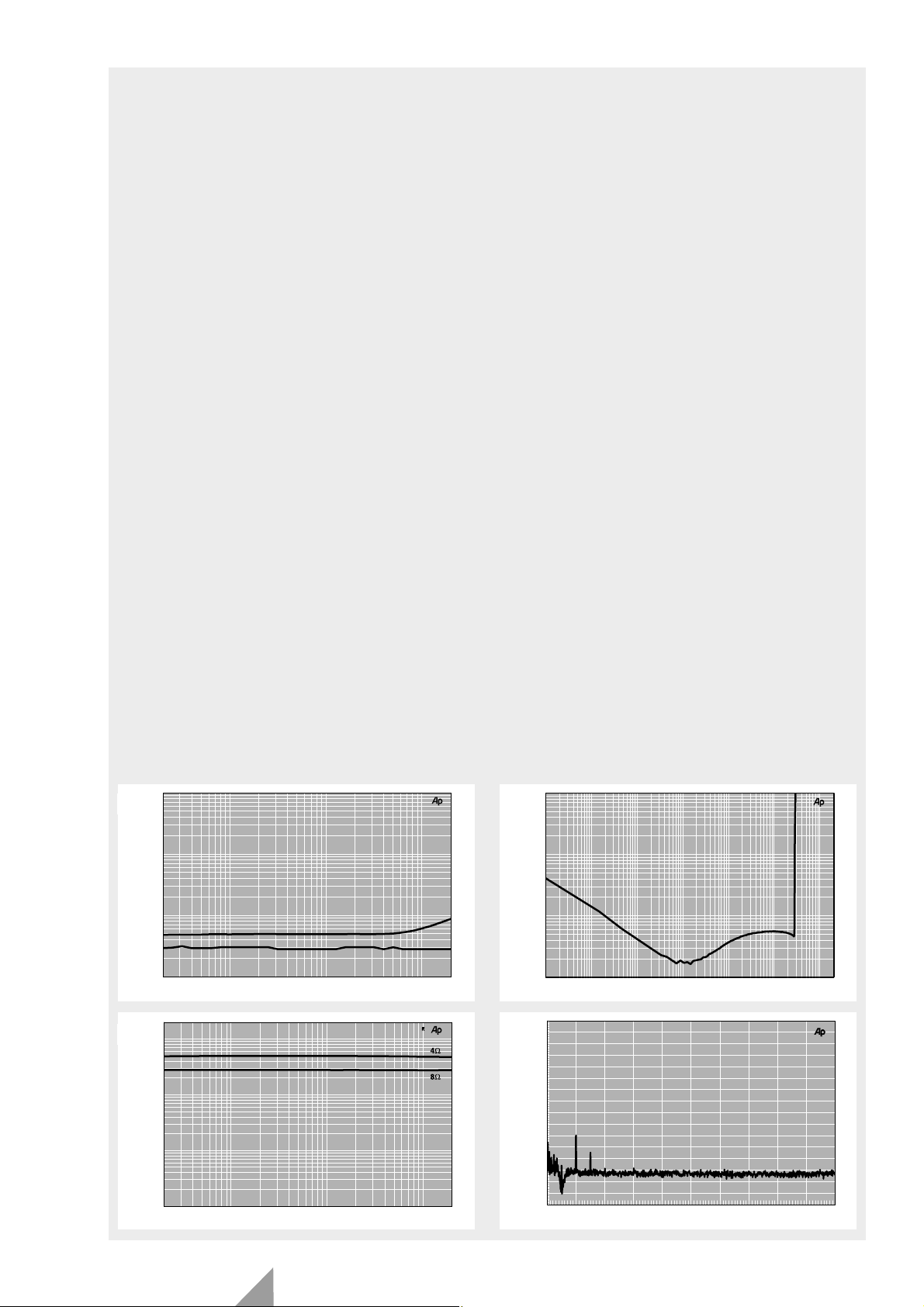
36
Elektor Electronics 5/99
Technical specifications
(Supply voltage = ±70 V; quiescent current = 200–400 mA)
Input sensitivity 1.1 V r .m.s.
Input impedance 47.5 kΩ
Sine-wave power output (0.1% THD) 280 W into 8 Ω; 500 W into 4 Ω; 800 W into 2 Ω
Music power* (1% THD) 300 W into 8 Ω; 550 W into 4 Ω; 1000 W into 2 Ω
Slew limiting 85 V µs
–1
Open-loop bandwidth 53 kHz
Open-loop amplification ×8600
Power bandwidth 1.5 Hz – 220 kHz
Signal-to-noise ratio (1 W into 8 Ω) 101 dB (A-weighted); 97 dB (B = 22 kHz)
Damping factor (at 8 Ω) >700 (1 kHz); >300 (20 kHz)
Output impedance 1.6 Ω
Harmonic distortion (THD) (B = 80 kHz) 8 Ω 4 Ω 2 Ω
at 1 kHz 0.003% (1 W) 0.0046% (1 W) 0.01% (1 W)
0.005% (200 W) 0.0084% (400 W) 0.02% (700 W)
at 20 kHz 0.009% (200 W) 0.018% (400 W) 0.07% (700 W)
Intermodulation distortion (IM)
(50 Hz:7 kHz = 4:1) 0.004% (1 W) 0.01% (1 W) 0.034% (1 W
0.016% (150 W) 0.025% (300W) 0.07% (500 W)
Dynamic IM
(square wave 3.15 kHz with sine wave 15 kHz) 0.003% (1 W) 0.0036% (1W) 0.0055% (1 W)
0.003% (200 W) 0.005% (400 W) 0.0085% (700 W)
*See Part 1 about the validity of this meaningless quantity.
The specified figures were measured after the amplifier
had been switched on for two hours. The figure show that
the Titan 2000 compares favourably with most amplifiers.
The slew limiting is a measure of the speed of the amplifier, which is exceptionally good in the Titan 2000.
Figure A shows the total harmonic distortion plus noise
(THD+N) for an output of 1 W into 8 Ω (lower curve) and
for 200 W into 8 Ω. The latter figure corresponds with 70%
of the peak sine wave power and the curve shows that the
distortion increases clearly only above 10 kHz.
Figure B shows the THD+N at 1 kHz as a function of the
drive with an output impedance of 8 Ω. The curve is pur-
posely drawn for a bandwidth of 22 kHz so that the noise
above 20 kHz does not degrade the performance of the
amplifier. From about 2 W, the distortion increases slightly
with increasing drive, which is normal in most amplifiers.
Figure C shows the peak output of the amplifier at a constant distortion of 0.1% and a load of 4 Ω (upper curve) and
8 Ω. The bandwidth was 80 kHz.
Figure D shows a Fourier analysis of a reproduced 1 kHz
signal at a level of 1 W into 8 Ω. It will be seen that the 2nd
harmonics are down just about 100 dB, while the 3rd harmonics are down to –114 dB. Higher harmonics lie below
the noise floor of –130 dB.
A B
C D
Contents
1
0.5
0.2
0.1
0.05
%
0.02
0.01
0.005
0.002
0.001
20 20k50 100 200 500 1k 2k 5k 10k
2k
1k
500
200
100
50
W
20
10
5
2
1
20 20k50 100 200 500 1k 2k 5k 10k
Hz
Hz
200W
1W
990001 - 3 - 14a
990001 - 3 - 14c
1
0.5
0.2
0.1
0.05
%
0.02
0.01
0.005
0.002
0.001
1m 2k2m 5m 10m 20m 50m 100m 500m 1 2 5 10 20 50 100 200 500 1k
+0
-10
-20
-30
-40
-50
-60
-70
d
-80
B
r
-90
-100
-110
-120
-130
-140
-150
-160
2k 20k4k 6k 8k 10k 12k 14k 16k 18k
W
Hz
990001 - 3 - 14b
990001 - 3 - 14d
 Loading...