


Development module for
STM32F407
Embedded Electronics
&
Solutions, s.r.o.
www.eeas.cz
T-Industry, s.r.o.
www.tind.sk
User guide


1. Key features
Processor
STM32F407VG
Power supply
5V
SD and SIM card slot
EEPROM
24LC256 (256kbit)
Ethernet
*
10/100 Mbit/s (DP83848)
USB
1x FTDI FT230XS and 1x STM32F4
CAN 2.0B*
SN65HVD230
RS232
GSM / GPRS*
Quectel M95
GPS*
Quectel L70
RF 434/868 MHz*
Radicrafts RC1180
Display
EADOGM163
Pressure sensor*
MPL3115A2
Accelerometer*
ADXL343
RTC
DS1339
LEDs
2 pcs + power LED
Buttons
2 pcs + reset button
Buzzer
1 pcs
*
optional peripherals
2. Front view
Ethernet USB FTDI
USB STM32F4
Power
GSM/GPRS
module
GPS
module
SWD
Interface
CAN
RS232
GPIO
pins
Reset
button
User
LEDs
User
buttons
Buzzer
RF module
Display
EEPROM
RTC
Accelerometer
Pressure
sensor

3. Bottom view
4. Block diagram
SD and SIM
card slot
S4
S6
S3 S5
5. Installation
5.1. Power supply
Use only included power supply adapter.
5.2. Software and drivers installation
We recommend to use CooCox CoIDE development studio. It is a free development
environment that is available at http://www.coocox.org. Installation process is
described on
http://www.coocox.org/book/coocox/coide-dev-manual/1-Quickstart.
After installing the CoIDE and setting the compiler you have to install the ST-Link/V2
driver that you can download on
http://www.st.com/web/en/catalog/tools/PF259459.
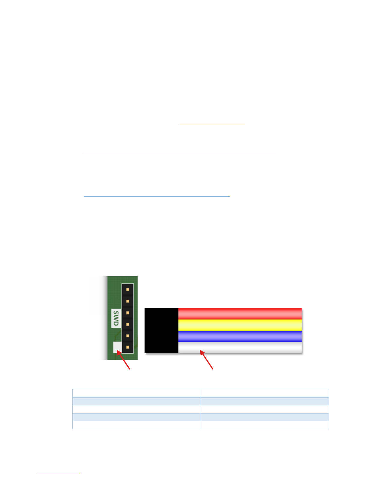
5.3. ST-Link/V2 programmer connection
The development board is supplied with an included ST-Link/V2 programmer. To
connection to the board use the SWD interface connector (see front view image in
the section 2). White wire refers to white mark printed on the board. (see image
below) Functions of individual programmer wires are given in the table below.
Wire color
Function
White
3V3
Blue
SWD CLK
Yellow
GND
Red
SWD IO
Programmer cableWhite mark

6. Peripherals description
6.1. GPIO
The development module contains 16 free GPIO
pins. They are directly connected to the header
(see front view image in the section 2). Their port
mapping is printed on the board (see detail).
6.2. Buttons
There are three buttons on the board. One reset button a two user buttons. Each
button is debounced using a pull-up resistor and a parallel capacitor (see schematic
below) and provides high logic level when is not pressed.
Signal name
Processor pin
Alternate function
RESET
NRST
SW0
PD15
SW1
PD14
Signal name
Processor pin
Alternate function
GPIO1
PE15
GPIO2
PE14
GPIO3
PE12
GPIO4
PE13
GPIO5
PE11
GPIO6
PE10
GPIO7
PE9 GPIO8
PE8 GPIO9
PB1
GPIO10
PB0 GPIO11
PA6 GPIO12
PA5
GPIO13
PA4
GPIO14
PA8 GPIO15
PA9 GPIO16
PA10
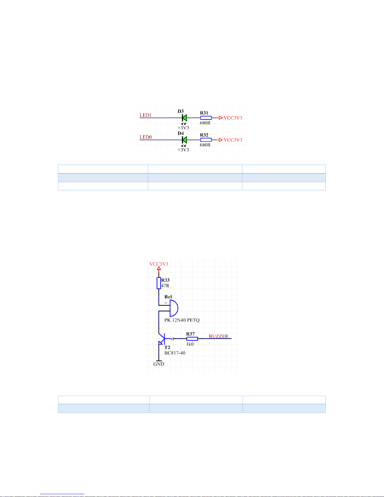
6.3. LEDs
The development module contains two user LEDs. They are connected
directly to the processor (see schematic below). Low level logic on the
corresponding pin turns LED on.
6.4. Buzzer
There is a buzzer on the board connected through the NPN transistor
(see schematic below).
Signal name
Processor pin
Alternate function
LED0
PD11
LED1
PD10
Signal name
Processor pin
Alternate function
BUZZER
PD12
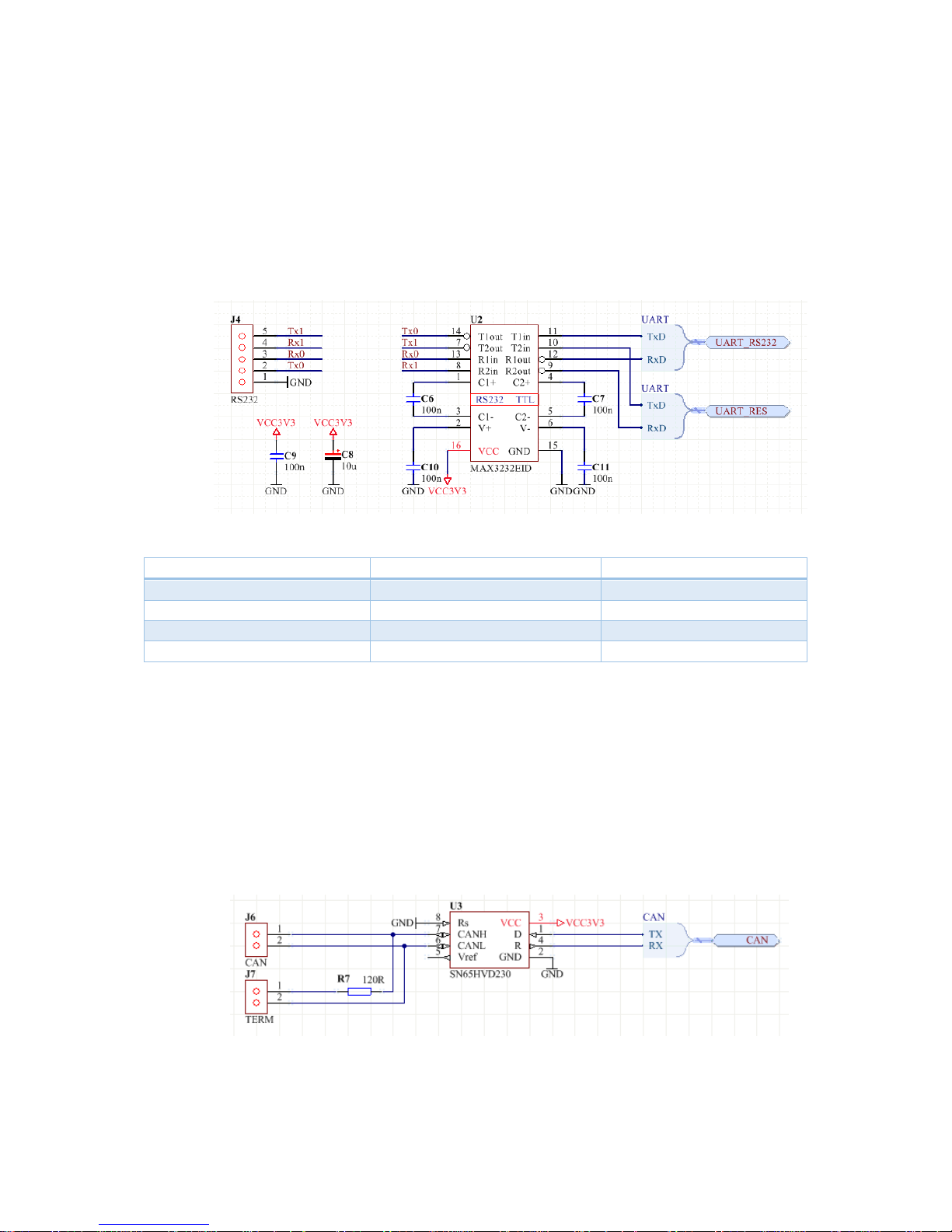
6.5. RS232
The development module is equipped with two RS232 interfaces using
MAX3232. Their signals are connected to the header J4 on the bottom
left side of the board (see front view image in the section 2). Electrical
connection is shown on the image below. The first pin of the header is
marked with a white rectangle printed on the board.
6.6. CAN (optional)
The board is optionally equipped with SN65HVD230 CAN transceiver. Its
signals are connected to the terminals on left side of the board (see
front view image in the section 2). 120 Ohm bus terminator can be
activated by plugging a jumper on the header J7 marked with label
TERM on the board (see schematic below).
Signal name
Processor pin
Alternate function
RS_TX0
PD8
USART3
RS_RX0
PD9
USART3
RS_TX1
PB15
RS_RX1
PB14

6.7. EEPROM
There is a 256 kbit EEPROM memory on the development module. The
memory is connected via common I2C interface (see schematic below).
The address pins are connected to GND so the slave address is 0x50.
6.8. RTC
The board is equipped with real time clock circuit. The RTC uses
common I2C interface (see schematic below). Its slave address is 0x68.
Pulses per second (PPS) output is directly connected to the processor.
Signal name
Processor pin
Alternate function
CAN_TX
PD1
CAN1
CAN_RX
PD0
CAN1
Signal name
Processor pin
Alternate function
SDA
PB9
I2C1
SCL
PB8
I2C1
Signal name
Processor pin
Alternate function
SDA
PB9
I2C1
SCL
PB8
I2C1
RTC_PPS
PE5

6.9. Accelerometer (optional)
The development module optionally contains digital accelerometer
ADXL343. The accelerometer uses common I2C interface (see schematic
below). Its INT1 is directly connected to the processor.
6.10. Pressure sensor (optional)
The development module is optionally equipped with MPL3115A2
pressure sensor. The sensor provides also temperature and altitude
measurement. It is connected via common I2C interface (see schematic
below). Its INT1 pin is directly connected to the processor.
Signal name
Processor pin
Alternate function
SDA
PB9
I2C1
SCL
PB8
I2C1
ACC_INT
PE0
Signal name
Processor pin
Alternate function
SDA
PB9
I2C1
SCL
PB8
I2C1
PRESS_INT
PE1

6.11. Display
There is an alphanumeric numeric display EADOGM163 with 16x3
characters on the board. Display connection is shown on the schematic
below. For detail information about communication interface please
see the attached datasheet. Display backlight is controlled using the BL
pin and the transistor T1.
6.12. GPS module (optional)
The development board is optionally equipped with Quectel L70B GPS
module. The module connection is shown on the image below. For
proper function pads S3 and S5 must be shorted and pads S4 and S6
must be opened (see bottom view image in the section 3).
Signal name
Processor pin
Alternate function
LCD_SI
PC13
LCD_CLK
PE6 LCD_RS
PC15
LCD_CSB
PC14
LCD_BL
PD13
Signal name
Processor pin
Alternate function
GPS_RF_TX
PD5
USART2
GPS_RF_RX
PD6
USART2

6.13. GPS / GPRS module (optional)
There is optionally Quectel M95 GPS / GPRS module on the board.
Module connection is shown on the image below. Power supply of the
module is initially switched off. To switch on the power supply apply
high logic level at signal GSM_ENABLE (PA0).
Signal name
Processor pin
Alternate function
GSM_ENABLE
PA0 GSM_TX
PB6
USART1
GSM_RX
PB7
USART1
GSM_PWK
PC0
GSM_STAT
PC3

6.14. SD card
SD card slot is directly connected to the processor via SDIO interface
(see schematic below).
6.15. RF module (optional)
The development module is optionally equipped with a RF module
manufactured by Radiocrafts. There are 434 MHz or 868 MHz versions
available. Module connection is shown on the image below. For proper
function pads S4 and S6 must be shorted and pads S3 and S5 must be
opened (see bottom view image in the section 3).
Signal name
Processor pin
Alternate function
SD_CLK
PC12
SDIO
SD_CMD
PD2
SDIO
SD_DAT0
PC8
SDIO
SD_DAT1
PC9
SDIO
SD_DAT2
PC10
SDIO
SD_DAT3
PC11
SDIO
Signal name
Processor pin
Alternate function
GPS_RF_TX
PD5
USART2
GPS_RF_RX
PD6
USART2

6.16. USB FTDI
There is a FTDI FT230XS USB to serial interface on the development
board. Schematic is shown on the image below.
6.17. USB STM
There is also USB OTG interface connected to separated connector
(see front view image in the section 2). Schematic is shown on the
image below.
Signal name
Processor pin
Alternate function
FTDI_TX
PC6
USART6
FTDI_RX
PC7
USART6
Signal name
Processor pin
Alternate function
USB_D+
PA12
OTG_FS
USB_D-
PA11
OTG_FS

6.18. Ethernet (optional)
The development board is optionally equipped with external 10/100
Mbit Ethernet transceiver DP83848. The transceiver uses the RMII
interface and its connection is shown in the attached schematic
documents.
Signal name
Processor pin
Alternate function
ETH_CLC
PA1
ETH_RMII
ETH_RESET
PA3
ETH_RMII
ETH_CRS
PA7
ETH_RMII
ETH_TXD_0
PB12
ETH_RMII
ETH_TXD_1
PB13
ETH_RMII
ETH_TX_EN
PB11
ETH_RMII
ETH_RX_0
PC4
ETH_RMII
ETH_RX_1
PC5
ETH_RMII
ETH_MDIO
PA2
ETH_RMII
ETH_MDC
PC1
ETH_RMII

7. Signal table
Signal name
Processor pin
Alternate function
ACC_INT
PE0 BUZZER
PD12
CAN_TX
PD1
CAN1
CAN_RX
PD0
CAN1
ETH_CLC
PA1
ETH_RMII
ETH_RESET
PA3
ETH_RMII
ETH_CRS
PA7
ETH_RMII
ETH_TXD_0
PB12
ETH_RMII
ETH_TXD_1
PB13
ETH_RMII
ETH_TX_EN
PB11
ETH_RMII
ETH_RX_0
PC4
ETH_RMII
ETH_RX_1
PC5
ETH_RMII
ETH_MDIO
PA2
ETH_RMII
ETH_MDC
PC1
ETH_RMII
FTDI_TX
PC6
USART6
FTDI_RX
PC7
USART6
GPIO1
PE15
GPIO2
PE14
GPIO3
PE12
GPIO4
PE13
GPIO5
PE11
GPIO6
PE10
GPIO7
PE9 GPIO8
PE8 GPIO9
PB1 GPIO10
PB0 GPIO11
PA6 GPIO12
PA5
GPIO13
PA4
GPIO14
PA8 GPIO15
PA9 GPIO16
PA10
GPS_RF_TX
PD5
USART2
GPS_RF_RX
PD6
USART2
GSM_ENABLE
PA0 GSM_TX
PB6
USART1
GSM_RX
PB7
USART1
GSM_PWK
PC0 GSM_STAT
PC3 LCD_SI
PC13
LCD_CLK
PE6 LCD_RS
PC15
LCD_CSB
PC14
LCD_BL
PD13
LED0
PD11
LED1
PD10
PRESS_INT
PE1

RESET
NRST
RS_TX0
PD8
USART3
RS_RX0
PD9
USART3
RS_TX1
PB15
RS_RX1
PB14
RTC_PPS
PE5 SD_CLK
PC12
SDIO
SD_CMD
PD2
SDIO
SD_DAT0
PC8
SDIO
SD_DAT1
PC9
SDIO
SD_DAT2
PC10
SDIO
SD_DAT3
PC11
SDIO
SDA
PB9
I2C1
SCL
PB8
I2C1
SW0
PD15
SW1
PD14
USB_D+
PA12
OTG_FS
USB_D-
PA11
OTG_FS

8. Notes


On behalf of
Embedded Electronics & Solutions, s.r.o.
we would like to thank you.
Manufacturer:
Embedded Electronics & Solutions, s.r.o.
Primátorská 296/38
180 00 Praha 8
info@eeas.cz
www.eeas.cz
Phone: +420 731480348 / +420 737980953
Distributor in Slovakia:
T-Industry, s.r.o.
Hoštáky 910/49
907 01 Myjava
tind@tind.sk
www.tind.sk
Phone: +421 907565722
 Loading...