

Page 1

LH185/216/236N99W SERVICE MANUAL
I
NDEX:
PART 1:Brief Introduction Of The LH185/216/236N99W
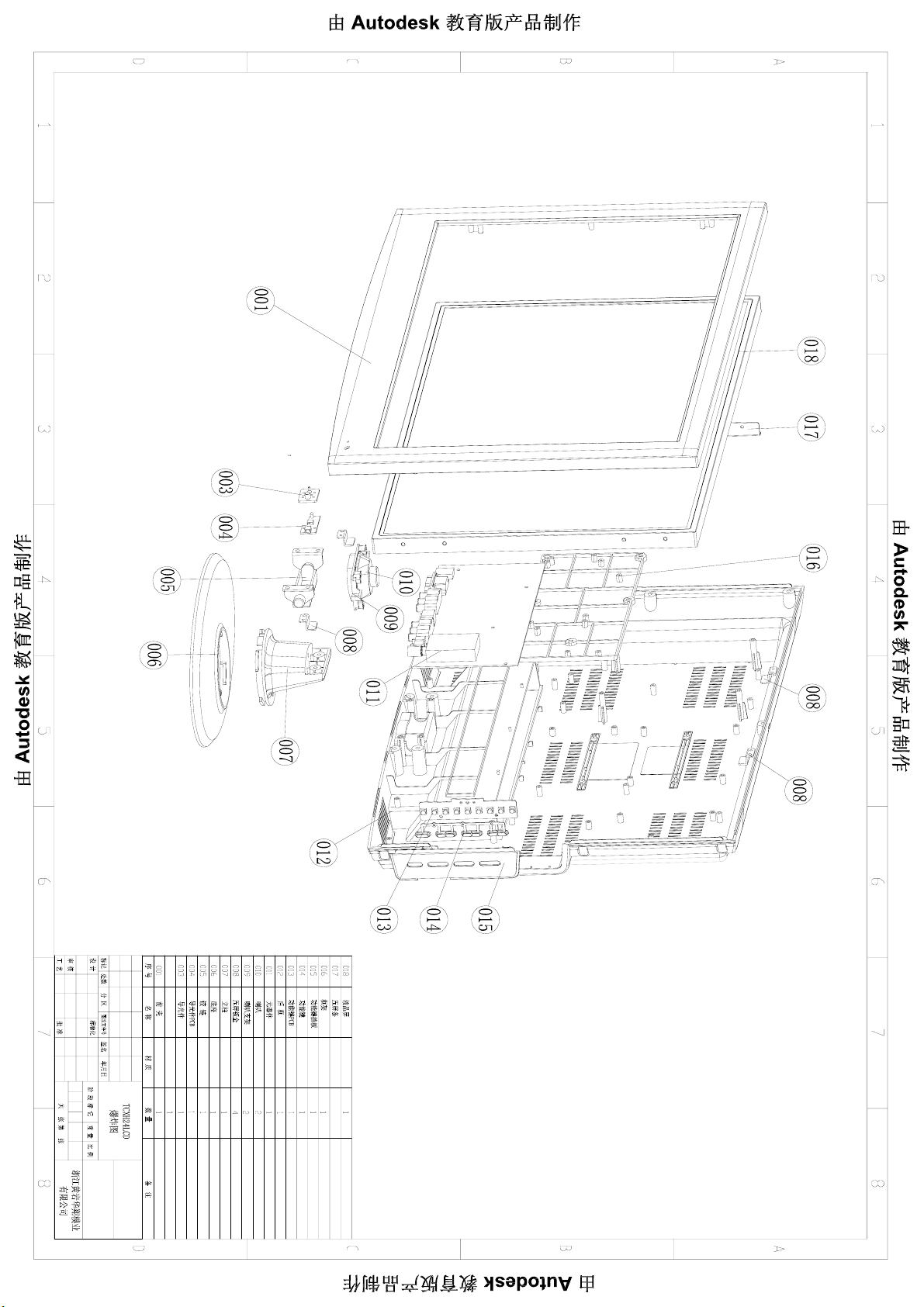
PART 2: Exploded view
PART 3: IC Introduction
PART 4: Detailed Circuit
PART 5: Components List
PART 6: Components
PART 7: Debug Instruction
Page 2
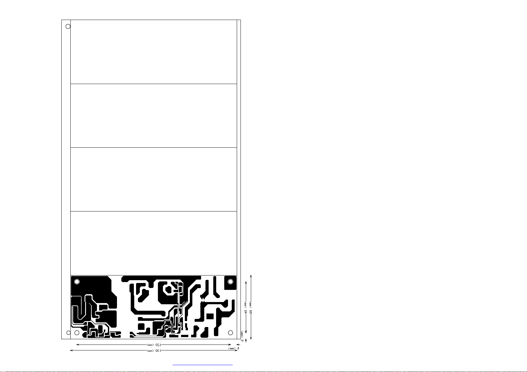
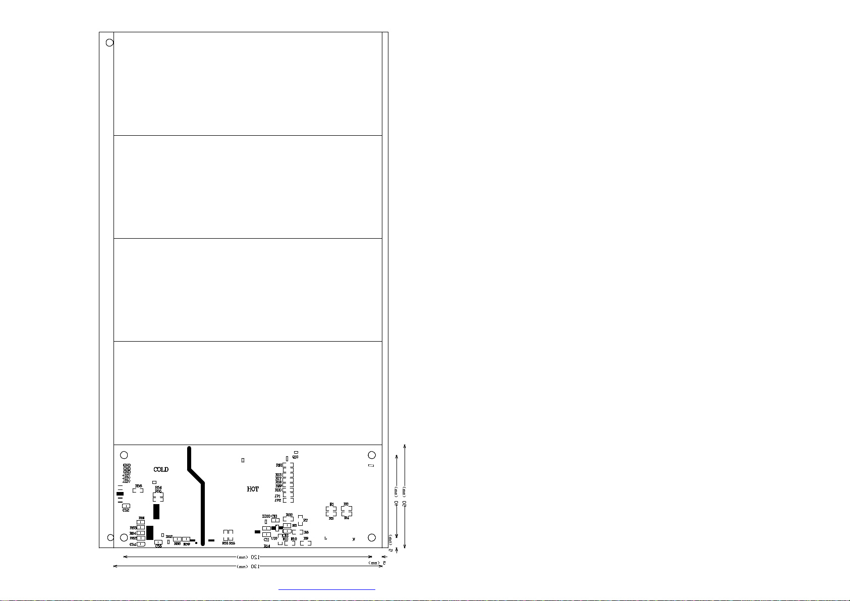
6. CONFIGURATION
z The PCB board is thick 1.6 mms
z Component the tallest altitude 16.5 mms
z Install diameter inside the bore 3.5 mms
All rights reserve, if the specification has fluctuation and take real object as quasi
10
Page 3
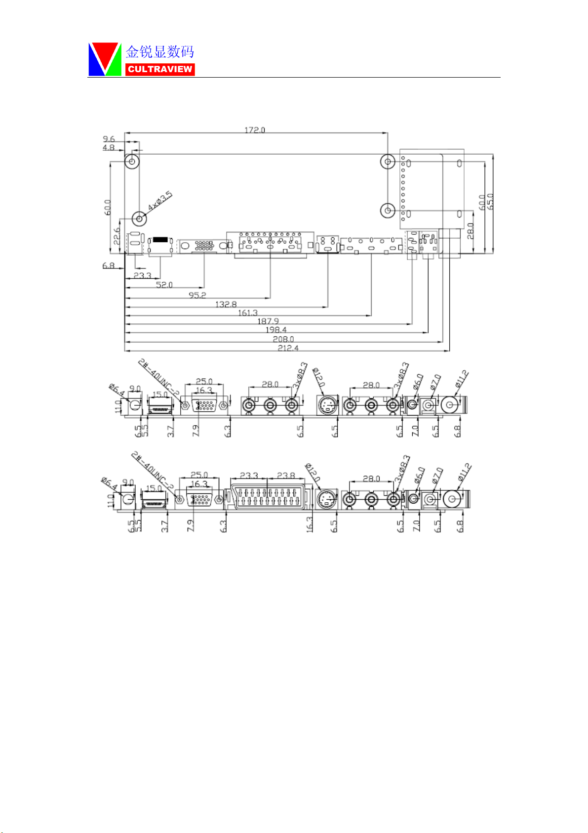
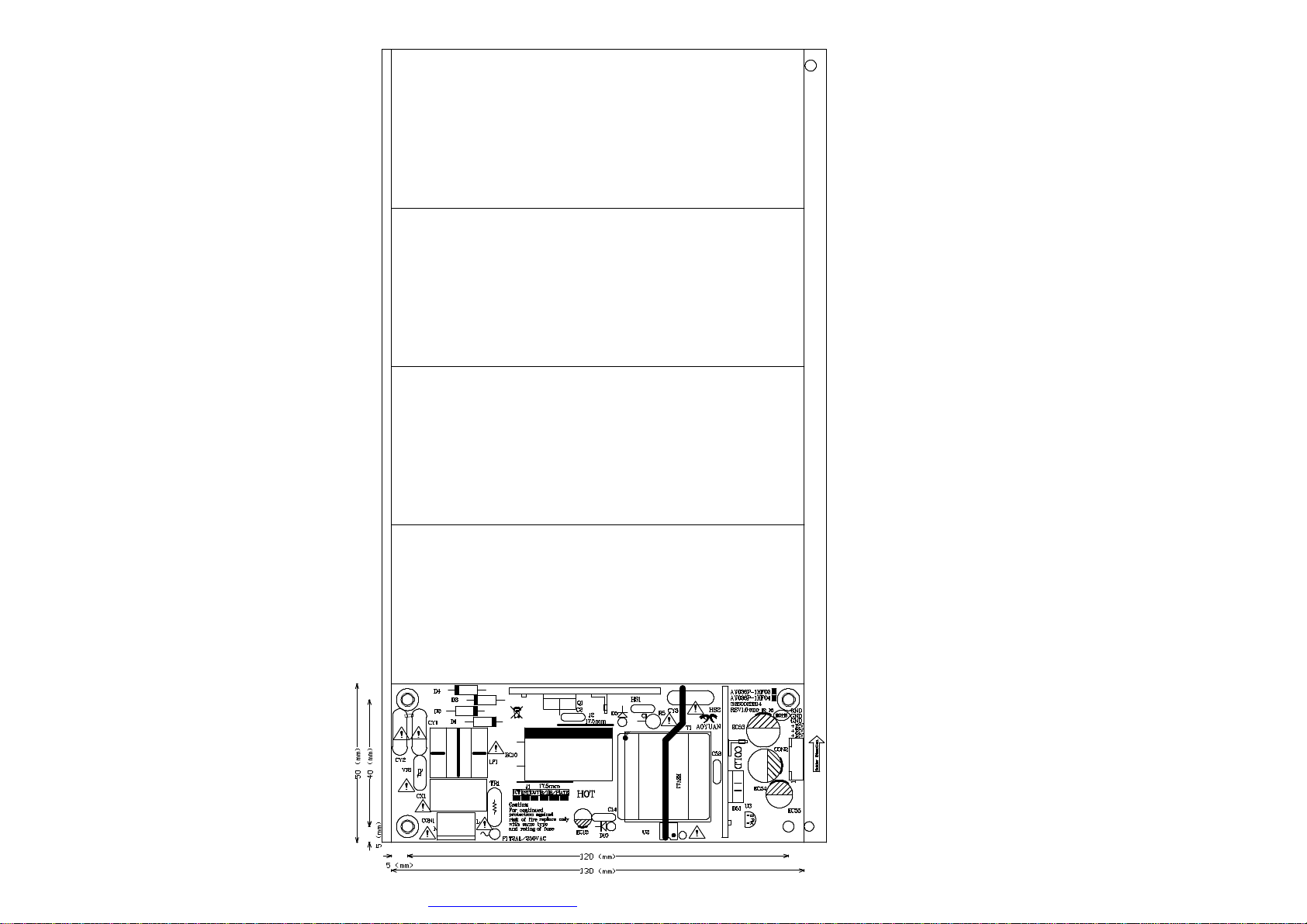
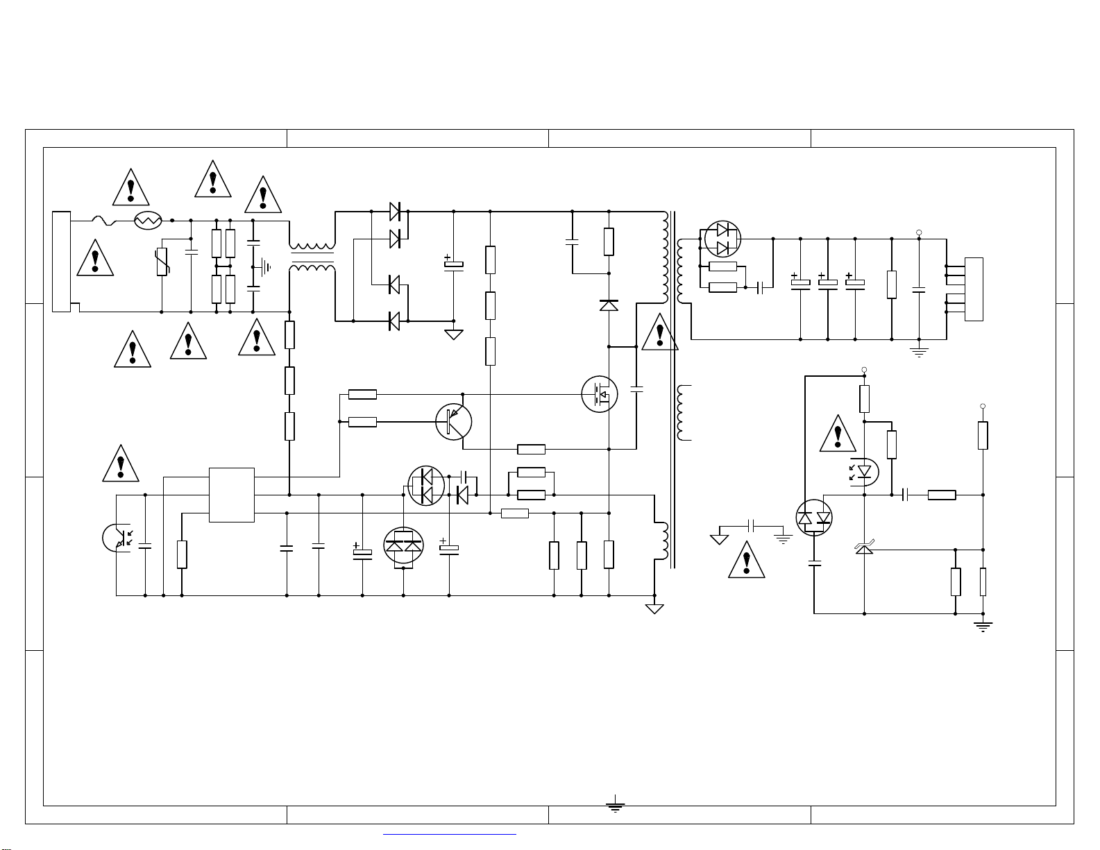
4. PICTURE
J5:INVE
RTER
J1:IR&KEY
BOARD
J3:PANEL
POWER
J2:LVDS
J6:AUDIO
OUT
J9:
HDMI
NOTE:J11 can be assembled with YPBPR or SCART .
J10:
VGA
J11:
SCART
J12:
S-VIDEO
J13:
AV
J14:PC
AUDIO
J15:EAR
PHONE
U12:
TUNER
All rights reserve, if the specification has fluctuation and take real object as quasi
6
Page 4
Page 5

Page 6
Page 7
PDF 文件使用 "pdfFactory Pro" 试用版本创建 www.fineprint.cn
Page 8
PDF 文件使用 "pdfFactory Pro" 试用版本创建 www.fineprint.cn
Page 9
PDF 文件使用 "pdfFactory Pro" 试用版本创建 www.fineprint.cn
Page 10
PDF 文件使用 "pdfFactory Pro" 试用版本创建 www.fineprint.cn
Page 11
5
+12V_I
J8
FUSEF1FUSE
DC-JACKJ8DC-JACK
+5V_SW
3
12
C25
C25
100uF/16V
100uF/16V
D D
C C
F1
1
1 2
2
12
C127
C127
100n
100n
+5Vsb_IN +3.3V_stb
CM1084
CM1084
U5
U5
CM1084
CM1084
3
VIN
VOUT
TAB
GND
1
620ma
CM1084
CM1084
U4
U4
CM1084
CM1084
3
2
VIN
VOUT
4
TAB
GND
1
<FUNCTION>
<FUNCTION>
2
4
<FUNCTION>
<FUNCTION>
220u/16v
220u/16v
包括了
C28
C28
220u/16v
220u/16v
C67
C67
100n
100n
20mA
C84
C84
1.26V的350MA
12
<FUNCTION>
<FUNCTION>
+12V_IN
12
C90
C90
470uF/16V
470uF/16V
1 2
TP6
TP6
1
TEST POINT
TEST POINT
12
C73
C73
100n
100n
1 2
+3.3V_SW
+5V_SW
TP4
TP4
1
TEST POINT
TEST POINT
D2 1N4001D2 1N4001
2 1
D1 1N4001D1 1N4001
2 1
4
+12V_IN
R51
R51
100K
100K
1 2
R870RR87
U7
1 2
C32
C32
3.3n
3.3n
R48
R48
2.2K
2.2K
U2
U2
3
VIN
C31
C31
100n
100n
12
12
L4FBL4
FB
1 2
BM1117-ADJ
BM1117-ADJ
BM1117-ADJ
BM1117-ADJ
VOUT
ADJ
1
TAB
8
7
6
5
VDDP_PM+3.3V_stb
AVDD_MPLL
C88
C88
10U/10V
10U/10V
2
4
100uF/16V
100uF/16V
<FUNCTION>
<FUNCTION>
0R
1 2
1
BS
SYNC
2
VIN
EN
3
VSW
COMP
4
12
GND
FB
C43
C43
1 2
100n
100n
12
C34
C34
C71
C71
9
PAD
100n
100n
MP1482U7MP1482
For PM Mode==>
VDDP_PM & AVDD_MPLL must be alive
1.4mA
6.8mA
12
C97
C97
C87
C87
1 2
100n
100n
100pF
100pF
TV 380mA
VCC1.26V
1
12
TP2
TP2
TEST POINT
TEST POINT
1 2
3
TP1
TP1
+5Vsb_IN
+5Vsb_IN
L5
C74
C74
10n
10n
33uH/2.5AL533uH/2.5A
+5Vsb_IN
1
12
12
R53
R53
12
C56
C56
470uF/16V
470uF/16V
12
C86
C86
68K_1%
68K_1%
100n
100n
R52
R52
15K_1%
15K_1%
1 2
WAKEUP
2
Power on =1
PM==> Power down(PM Mode)=0
WAKEUP
R58
R58
4.7k
4.7k
R59
R59
1 2
4.7k
4.7k
1
1 2
1 2
Q9
3904Q93904
2 3
L1 2A/0805/NCL1 2A/0805/NC
1 2
Q11
Q11
12
+12V
AO3401
AO3401
312
C45
C45
1u
1u
+5Vsb_IN
R4
47kR447k
1 2
R3
2.2kR32.2k
1 2
1
Q3
3904Q33904
2 3
5VA_A
L11FBL11
FB
1 2
12
L10 FB/NCL10 FB/NC
1 2
Q2 AO3401Q2 AO3401
C2
C2
1u
1u
+5V_SW
312
+12V_IN
R70
R70
47k
47k
R61
R61
20k
20k
12
1
+3.3V_SW
B B
+3.3V_SW
A A
1 2
5
AVDD_AU
AVDD_VIF
L6FBL6
FB
C81
C81
10u
10u
AVDDA
12
C26
C26
10U/10V
10U/10V
14mA
C76
C76
1 2
100n
100n
142mA
12
12
C95
C95
C80
C80
1 2
100n
100n
100pF
100pF
VDDP
295mA 78mA
C115
C115
C22
C22
C89
C89
C55
C55
1 2
1 2
1 2
1 2
100n
100n
100n
100n
100n
100n
100n
100n
VCC1.26V VDDC
C46
C46
1 2
100n
100n
C35
C35
C109
C109
1 2
1 2
100n
100n
100n
100n
4
A2
AHOLE138A2AHOLE138
380mA
C39
C39
C62
C62
C23
C23
1 2
1 2
1 2
100n
100n
100n
100n
100n
100n
+5Vsb_IN
12
+5Vsb_IN
R33
A4
A1
A3
AHOLE138A4AHOLE138
AHOLE138A1AHOLE138
AHOLE138A3AHOLE138
1
1
1
1
3
5VA_A
<FUNCTION>
<FUNCTION>
NC
NC
6
6
5
5
4
4
3
3
2
2
POWER1_ON/OFF WAKEUP
1
1
J16
J16
TOP TEST POINT
M9
1
TPADM9TPAD
BUTTOM TEST POINT
M13
M13
1
TPAD
TPAD
+5Vsb_IN
1
POWER1_ON/OFF
C118
C118
100n/NC
100n/NC
M8
1
TPADM8TPAD
M12
M12
M6
1
TPAD
TPAD
TPADM6TPAD
2
R33
12
1k/NC
1k/NC
R13
R13
1 2
R32 NC/0RR32 NC/0R
12
Q29
Q29
3904/NC
3904/NC
2 3
M5
1
TPADM5TPAD
10k/NC
10k/NC
1
R56 4.7k/NCR56 4.7k/NC
Q28
Q28
1
3904/NC
3904/NC
12
01_POWER
01_POWER
01_POWER
CVMV26L-A-4
CVMV26L-A-4
CVMV26L-A-4
H:ON
L:OFF
CONFIDENTIAL
CONFIDENTIAL
CONFIDENTIAL
1
2 3
Cultraview , Inc.
Cultraview , Inc.
Cultraview , Inc.
Title
Title
Title
Size Document Number Rev
Size Document Number Rev
Size Document Number Rev
C
C
C
Date: Sheet of
Date: Sheet of
Date: Sheet
0
0
0
28Friday, April 15, 2011
28Friday, April 15, 2011
28Friday, April 15, 2011
3000 LongDong Road
3000 LongDong Road
3000 LongDong Road
Shanghai,China
Shanghai,China
Shanghai,China
(86) 021-68791101
(86) 021-68791101
(86) 021-68791101
of
V1.0
V1.0
V1.0
Page 12
5
4
3
2
1
SDA_HD
SCL_HD
B_TX0+
B_TX0G_TX1+
G_TX1R_TX2+
R_TX2TXCLK+
TXCLK-
HD5V
12
C144
C144
100n
100n
24C02=>EDID code must
be upto 256byte space,
for HDMI interface.
SDA_HD
SCL_HD
B_TX0+
B_TX0G_TX1+
G_TX1R_TX2+
R_TX2TXCLK+
TXCLK-
HDMI
J9
20
GND0
21
GND1
22
D D
C C
B B
GND2
GND3
CEC/DDC GND
DDC SCL
DDC SDA
Dat2 shield
Dat1 shield
Dat0 shield
clk shield
DAT0+
DAT0-
DAT1+
DAT1-
DAT2+
DAT2-
HDMIJ9HDMI
HD5V
RX_0+
RX_0RX_1+
RX_1RX_2+
RX_2-
RX_C+
RX_C-
HD5V
DDC_CLK_IN
DDC_DAT_IN
HPD
HD5V
23
18
+5V
17
15
16
13
CEC
19
HPD
2
5
8
11
7
9
4
6
1
3
10
clk+
12
clk-
14
NC1
R161
R161
R160
R160
10K
10K
10K
10K
1 2
1 2
D10
D10
1N4148
1N4148
<FUNCTION>
<FUNCTION>
R140 100RR140 100R
1 2
R141 100RR141 100R
1 2
R165 0RR165 0R
1 2
R164 0RR164 0R
1 2
R167 0RR167 0R
1 2
R166 0RR166 0R
1 2
R169 0RR169 0R
1 2
R168 0RR168 0R
1 2
R163 0RR163 0R
1 2
R162 0RR162 0R
1 2
21
HOTPLUG
R1701KR170
1K
1 2
HPD
R133 4.7KR133 4.7K
1 2
1
3904
3904
2 3
Q24
Q24
R134
R134
10K
10K
1 2
HPLUG
HPLUG
A A
Cultraview , Inc.
Cultraview , Inc.
Cultraview , Inc.
Title
Title
Title
02.HDMI Interface
02.HDMI Interface
02.HDMI Interface
Size Document Number Rev
Size Document Number Rev
Size Document Number Rev
B
B
B
Date: Sheet of
Date: Sheet of
5
4
3
2
Date: Sheet
CONFIDENTIAL
CONFIDENTIAL
CONFIDENTIAL
CVMV26L-A-4
CVMV26L-A-4
CVMV26L-A-4
3000 LongDong Road
3000 LongDong Road
3000 LongDong Road
Shanghai,China
Shanghai,China
Shanghai,China
(86) 021-68791101
(86) 021-68791101
(86) 021-68791101
0
0
0
38Friday, April 15, 2011
38Friday, April 15, 2011
38Friday, April 15, 2011
1
V1.0
V1.0
V1.0
of
Page 13
VGA
D D
+5Vsb_IN
SCART_AVOUT
+5V_SW
C C
CVBSOut1
YC
J12 SVIDEOJ12 SVIDEO
SCART
B B
J11
J11
SCART
SCART
A A
5
1617
VGA_RX
1
11
6
2
12
7
3
13
8
VGA_TX
4
14
9
5
15
10
J10
J10
VGA
VGA
R187 4.7KR187 4.7K
1 2
R194 4.7KR194 4.7K
1 2
12
C135
C135
100n
100n
U13
U13
1
NC1
VCC
2
NC2
VCLK
3
NC3
SCL
GND4SDA
24C02/NC
24C02/NC
C60
C60
100n
100n
R150
R150
1 2
22k
22k
1 2
C128
C128
1
12
10u/25V
10u/25V
R149
R149
10k
10k
1 2
S_Y
31
1 2
S_C
1 2
42
12
12
12
C139
C139
L8 2.2uHL8 2.2uH
220p
220p
L9 2.2uHL9 2.2uH
765
C137
C137
220p
220p
C141
C141
C138
C138
220p
220p
220p
220p
SHIELD
SHIELD
21
V_IN
V_IN
20
V_OUT
V_OUT
19
18
17
16
15
DATAGND
DATAGND
14
13
12
11
10
9
SWTCH
SWTCH
8
7
6
5
4
A_OUT_L
A_OUT_L
3
2
A_OUT_R
A_OUT_R
1
AV_OUT
BLANKGND
BLANKGND
VGND
VGND
BLANK
BLANK
R
R
SCART_R
RGND
RGND
DATA
DATA
G
G
SCART_G
CLKOUT
CLKOUT
GGND
GGND
AUDIO/RGB/16:9
B
B
SCART_B
A_IN_L
A_IN_L
SCART-L
R158 10kR158 10k
1 2
BGND
BGND
AGND
AGND
SCART_LOUT
SCART_LOUT
A_IN_R
A_IN_R
SCART-R
SCART_ROUT
SCART_ROUT
12
12
C132
C132
C134
C134
22n
22n
22n
22n
12
12
12
R198
R198
R199
R199
R200
R200
75R
75R
75R
75R
75R
75R
R-
GB-
DDC_SCL
VGA_RX
DDC_SCL
DDC_SDA
VGA_TX
DDC_SDA
8
7
6
5
R152
R152
220R
220R
Q23
Q23
1
1 2
3906
3906
Q22
Q22
3 2
3904
3904
AV_OUT
R155 220RR155 220R
R156 75RR156 75R
12
12
2 3
R172
R172
75R
75R
1 2
R128 33RR128 33R
C116 47nFC116 47nF
1 2
1 2
SV_Y0
R129 33RR129 33R
1 2
1 2
SV_C0
C117 47nFC117 47nF
12
12
12
R17575RR17575R
R17375RR17375R
C120
C120
R131
R131
CVBS0AV2
33R
33R
1 2
12
47nF
47nF
R196
R196
75R
75R
FB
12
SCART_G
R17175RR17175R
SCART_R
SCART_B
AV_MODE
12
R147
R147
2.7k
2.7k
R139
R139
SCART-L
C149
C149
22pF
22pF
SCART-R
C148
C148
22pF
22pF
Close to connector
R127 10R127 10
R
1 2
G
R126 0RR126 0R
1 2
B
R125 10R125 10
1 2
R123 10R123 10
1 2
RXD
R222 NCR222 NC
1 2
RXD
R223 0RR223 0R
1 2
TXD
R234 NCR234 NC
1 2
TXD
R239 0RR239 0R
1 2
R1424.7k R1424.7k
R1454.7k R1454.7k
12
12
+5Vsb_IN
CVBS0
C105 1nC105 1n
R119 0RR119 0R
1 2
1 2
R120 33RR120 33R
C106 47nFC106 47nF
1 2
1 2
C108 47nFC108 47nF
R122 33RR122 33R
1 2
1 2
R118 33RR118 33R
C104 47nFC104 47nF
1 2
1 2
12
12
12
R157
R157
R148
R148
75R
75R
75R
75R
75R
75R
C66
C66
R193
R193
12
1 2
10K
10K
12
R192
R192
12
10K
10K
1u
1u
12
C143
C143
R182
R182
560pF
560pF
12K
12K
1 2
C63
C63
1 2
12
12
R181
R181
1u
1u
C142
C142
12K
12K
560pF
560pF
1 2
Close to MST IC
C113 1nC113 1n
C112
C112
C114 47nFC114 47nF
C110 47nFC110 47nF
SOY
1 2
1 2
1 2
1 2
RIN+
SOG
47nF
47nF
GIN+
BIN+
close to MST IC
R189 100RR189 100R
1 2
R191 100RR191 100R
1 2
12
12
R197
R197
R190
R190
2.2K
2.2K
2.2K
2.2K
J7
J7
AV3-8R4-5
AV3-8R4-5
L
L
6
5
R
R
4
3
V
V
2
1
SOY
Y+
PR+
PB+
AV_AUL2
AV_AUR2
4
3
2
1
PC audio Input
J14
J14
GND
GND
1
AUDIO_R
AUDIO_R
3
5
4
2
AUDIO_L
AUDIO_L
PHONOJACK
PHONOJACK
HS_RGB
V_RGB
AV_AUDIO&VIDEO Input
SCART_R
SCART_B
SCART_G
R180 10KR180 10K
12
12
C147
C147
22pF
22pF
R202 10KR202 10K
12
C151
C151
22pF
22pF
AV_RIN
AV_LIN
CVBS_1
J13
J13
AV3-8R4-5
AV3-8R4-5
L
L
AV_RIN
6
5
R
R
AV_LIN
4
3
V
V
CVBS_1
2
1
V_RGB
FB
1
AUDIO_SEL
C70
C70
PC_R
1 2
10K
10K
R186
R186
10K
10K
R130
R130
33R
33R
1 2
AV_AUR1
1u
1u
C72
C72
PC_L
1 2
AV_AUL1
1u
1u
C77
C77
12
1 2
PC_AUR0
12
R185
R185
C146
C146
1u
1u
12K
12K
560pF
560pF
1 2
C78
C78
1 2
12
PC_AUL0
12
1u
1u
R183
R183
C145
C145
12K
12K
560pF
560pF
1 2
1 2
CVBS1
C119
C119
47nF
47nF
C140 NCC140 NC
1 2
Q25
Q25
3904
3904
23
1
Q26
Q26
3906
3906
32
VS_RGB
1
12
C136
C136
R159
R159
560pF
560pF
12K
12K
1 2
12
12
C150
C150
R201
R201
560pF
560pF
12K
12K
1 2
R184
R184
1 2
R179
R179
75R
75R
R174 NC R174 NC
R195 1k R195 1k
1 2
+12V
R203
R203
10k
10k
R188 100k R188 100k
1 2
1 2
Q27
Q27
3904
3904
2 3
High (1-3V) - RGB / Low (0-0.4V) - Composite
5
4
3
2
Cultraview , Inc.
Cultraview , Inc.
Cultraview , Inc.
Title
Title
Title
03.Video&AudioInterface
03.Video&AudioInterface
03.Video&AudioInterface
Size Document Number Rev
Size Document Number Rev
Size Document Number Rev
D
D
D
Date: Sheet
Date: Sheet
Date: Sheet
1
CONFIDENTIAL
CONFIDENTIAL
CONFIDENTIAL
CVMV26L-A-4
CVMV26L-A-4
CVMV26L-A-4
0
0
0
3000 LongDong Road
3000 LongDong Road
3000 LongDong Road
Shanghai,China
Shanghai,China
Shanghai,China
(86) 021-68791101
(86) 021-68791101
(86) 021-68791101
48Friday, April 15, 2011
48Friday, April 15, 2011
48Friday, April 15, 2011
of
of
of
V1.0
V1.0
V1.0
Page 14
5
D D
7805/500MA
+12V
12
C52
C52
100uF/16V
100uF/16V
C C
12
13
14
15
F21WT-3DAR-E
F21WT-3DAR-E
U12
U12
B B
7805/500MA
U6
U6
+5V_IN_TUNER
LM340
LM340
1
3
VIN
VOUT
C33
C33
GND
TAB
<FUNCTION>
<FUNCTION>
2
4
12
GND1
GND2
GND3
GND4
220uF/16V
220uF/16V
C58
C58
100n
100n
IF_TV
11
IF
10
NC5
9
NC4
8
ADC
7
+5V
6
NC2
5
SDA
4
SCL
3
AS
2
NC1
AGC
1
AGC
12
<FUNCTION>
<FUNCTION>
12
TP5
TP5
1
TEST POINT
TEST POINT
12
C30
C30
100n
100n
R28
R28
NC
NC
+5V_IN_TUNER
1 2
R85 10 R85 10
1 2
R89 10 R89 10
12
12
C64
C64
C75
C75
22pF
22pF
22pF
22pF
R111
R111
100R
100R
4
Layout placement
Close to Tuner
+12V VIF_12V
R37
R37
150R/NC
150R/NC
12
C59
C59
C21
C21
100n
100n
100uF/16V/NC
100uF/16V/NC
IF_TV
C20
C20
10nF
10nF
I2C_SDA
I2C_SCL
D7
1N4148D71N4148
R94
R94
12K
12K
C101
C101
1 2
100n
100n
VIF_12V
12
C14
C14
C12
C12
R31
R31
10nF
10nF
2.2u
2.2u
1 2
1 2
6.8K
6.8K
1 2
R360RR36
0R
C150RC15
0R
R340RR34
12
0R
R271KR27
1K
TAGC
Q6
2SC2717Q62SC2717
TAGC
L2
0.82uHL20.82uH
1
3
P+S R101=NC R134=0R
12
R35
R35
680R
680R
32
R44
R44
22R
22R
12
C100
C100
10nF
10nF
1 2
C103
C103
10nF
10nF
R109
R109
6.8K
6.8K
R107
R107
6.8K
6.8K
+5V_IN_TUNER
R116
R116
6.8K
6.8K
R112
R112
6.8K
6.8K
+5V_IN_TUNER+5V_IN_TUNER
R95
R95
3.3K
3.3K
R990RR99
0R
R115
R115
6.8K
6.8K
R117NCR117
NC
P+N R101=0R R134=NC
NTSC R101=NC R134=NC
layout placement
Close to Mstar IC
use for two standard audio system.
this is for PAL BG/DK/I,SECAM L &
switch L'.
U10
U10
K9352
K9352
1
IN
D8
BAV277D8BAV277
ING2OUT1
Q18
Q18
R100 NCR100 NC
1
3904
3904
2 3
U11
U11
K7262
K7262
1
SAW
SAW
D9
BAV277D9BAV277
ING2OUT1
GND
3
Q19
Q19
R101 10KR101 10K
SIF_CTL
1
3904
3904
2 3
2
SIF
OUT2
SAW
SAW
GND
3
OUT25IN
4
SIFP
5
4
SIF_CTL
SIFP
SIF
SIFM
SIFM
SIF_CTL
VIFM
VIFM
VIF
VIFP
VIFP
1
A A
Cultraview , Inc.
Cultraview , Inc.
Cultraview , Inc.
Title
Title
Title
04.IF Interface
04.IF Interface
04.IF Interface
Size Document Number Rev
Size Document Number Rev
Size Document Number Rev
C
C
C
Date: Sheet of
Date: Sheet of
5
4
3
2
Date: Sheet
CONFIDENTIAL
CONFIDENTIAL
CONFIDENTIAL
CVMV26L-A-4
CVMV26L-A-4
CVMV26L-A-4
1
0
0
0
58Friday, April 15, 2011
58Friday, April 15, 2011
58Friday, April 15, 2011
3000 LongDong Road
3000 LongDong Road
3000 LongDong Road
Shanghai,China
Shanghai,China
Shanghai,China
(86) 021-68791101
(86) 021-68791101
(86) 021-68791101
of
V1.0
V1.0
V1.0
Page 15

5
+3.3V_stb
3
D5
D5
BAV99
BAV99
12
R80
R80
1
2
12
C37
C37
100n
R66 4.7KR66 4.7K
DVI/HDMI
VGA
Y,Pb,Pr
VIDEO
AUDIO
R501KR50
1K
100n
Q15
Q15
1
12
3906
3906
R76
R76
SYS_RST
HWRESET
12
3 2
100R
100R
R73
R73
12
22K
22K
TXCLKTXCLK+
B_TX0B_TX0+
G_TX1G_TX1+
R_TX2-
R_TX2+
SDA_HD
SCL_HD
INPUT
HS_RGB
VS_RGB
BIN+
SOG
INPUT
GIN+
RIN+
PR+
SOY
Y+
PB+
INPUT
CVBS0
SV_C0
SV_Y0
CVBS1
CVBSOUT1
INPUT
PC_AUL0
PC_AUR0
AV_AUL1
AV_AUR1
AV_AUL2
AV_AUR2
AUDIO
INPUT
AUOutL1_amp
AUOutR1_amp
OUTPUT
VIFP
VIFM
SIFP
SIFM
VIF
INPUT
+3.3V_SW
1 2
ADJ_PWM
C441nC44
1n
1 2
TXCLKTXCLK+
B_TX0B_TX0+
G_TX1G_TX1+
R_TX2R_TX2+
SDA_HD
SCL_HD
HPLUG
HPLUG
HS_RGB
VS_RGB
BIN+
SOG
GIN+
RIN+
PR+
SOY
Y+
PB+
CVBS0
+5V_IN_TUNER
SV_C0
SV_Y0
CVBS1
CVBSOut1
PC_AUL0
PC_AUR0
AV_AUL1
AV_AUR1
COMP_AUL2
COMP_AUR2
AUOutL2
AUOutL2
AUOutR2
AUOutR2
AUOutL1_amp
AUOutR1_amp
VIFP
VIFM
SIFP
SIFM
TAGC
TAGC
AV_MODE
AV_MODE
R571KR57
1K
PWM2
PWM1PWM1
PWM1
SPI_CZ
SPI_DI
SPI_DO1
100K
100K
D D
12
C38
C38
10u
10u
C C
B B
Mode
Selection
+3.3V_SW
1 2
PWM0
FB
1 2
R55 1KR55 1K
1 2
C96
C96
CL=20pf of XTAL
27pF
27pF
1 2
12
12
14.318MHZX114.318MHZ
X1
R1101MR110
3
1M
C98
C98
27pF
27pF
1 2
R121 68RR121 68R
R124 68RR124 68R
R132 68RR132 68R
WARNING !!!
Please close
to chip.
L3FBL3
TAGC
12
12
12
R88
R88
C82
C82
4.7K
4.7K
100n
100n
C48
C48
100n
100n
R82 0RR82 0R
C61
C61
C65
C65
10u
10u
1 2
100n
100n
1 2
+3.3V_SW
12
R6
10KR610K
CZ
SO
C27NCC27
NC
1 2
SCKSPI_CK
78
7531
8642
7531
8642
CZ
RP6
RP6
56
SI
RP22X4
RP22X4
34
SO
12
R103 470RR103 470R
12
SCL_HD
111
DDCDB_CK
SDA_HD
112
DDCDB_DA
TXCLK-
119
RXACKN
TXCLK+
120
RXACKP
B_TX0-
121
RXA0N
B_TX0+
122
RXA0P
G_TX1-
124
RXA1N
G_TX1+
125
RXA1P
HPLUG
126
HPLUGA
R_TX2-
127
RXA2N
R_TX2+
128
RXA2P
PB+
2
BIN1
SOY
3
SOGIN1
Y+
4
GIN1
C107 47nFC107 47nF
12
12
5
GIN1M
PR+
6
RIN1
HS_RGB
8
HSYNC0
BIN+
9
BIN0
C111 47nFC111 47nF
10
12
12
GIN0M
GIN+
11
GIN0
SOG
12
SOGIN0
RIN+
13
RIN0
VS_RGB
14
VSYNC0
SV_C0
16
CVBS3P
SV_Y0
17
CVBS2P
CVBS1
18
CVBS1P
CVBS0
19
CVBS0P
C121 47nFC121 47nF
20
12
12
C85
C85
1 2
C83 100nC83 100n
12
C79
C79
100pF
100pF
12
12
C51
C51
10U/10V
10U/10V
U3
MX25L8005U3MX25L8005
1
CE#
2
SO
3
WP#
VSS4SI
12
C19NCC19
NC
VCOM0
CVBSOut1
21
CVBSOUT
VIFP
30
VIFP
VIFM
31
VIFM
SIFM
32
SIFM
SIFP
10u
10u
33
SIFP
12
35
VR27
37
TAGC
PC_AUL0
39
LINE_IN_2L
PC_AUR0
40
LINE_IN_2R
AV_AUL1
41
LINE_IN_3L
AV_AUR1
42
LINE_IN_3R
AV_AUL2
43
LINE_IN_4L
AV_AUR2
44
LINE_IN_4R
C57 100nC57 100n
12
45
AUCOM
AUVRADN
46
AUVRM
AUVRADP
47
AUVRP
AUVREF
48
AUVREF
AUOutL1_amp
C53
C53
50
DAC_OUT_0L
AUOutR1_amp
51
DAC_OUT_0R
AUOutL2
100n
100n
52
1 2
LINE_OUT_0L
AUOutR2
53
LINE_OUT_0R
+3.3V_SW
12
C11
C11
100n
100n
8
VDD
7
HOLD#
SCK
6
SCK
SI
5
HWRESET
24
113
25
XIN
XOUT
HWRESET
GND01GND922GND7
GPIO Control Pins
ON-PANEL
WAKEUP
LED
AUDIO_SEL
ON-PBACK
AMP-MUTE
4
VDDP_PM
AVDD_MPLL
AVDDA VDDPVDDC
110
23
123
VDDP_2
AVDD_DVI
AVDD_MPLL
TSUMV26KU
TSUMV26KU
GND4
GND6
GND5
GND8
GND358GND11
29
55
34
49
26
L7FBL7
FB
1 2
+5V_SW
12
GPIOD[0]
ALE
3
AVDD_VIF
AVDD_AU
38
90
64
57
102
56
116
7
78
118
54
36
15
VDDC3
AVDD_ADC
AVDD_ADC1
U8
U8
GND263GND1
GND10
79
117
101
R81
R81
4.7K
4.7K
28
VDDP4
VDDP3
VDDP2
VDDP5
VDDP1
VDDP6
VDDC2
VDDC1
AVDD_AU
AVDD_VIF127AVDD_VIF3
AVDD_VIF2
XO0-
100
LVA0P
XO0+
99
LVA0M
XO1-
98
LVA1P
XO1+
97
LVA1M
XO2-
96
LVA2P
XO2+
95
LVA2M
XOC-
94
LVACKP
XOC+
93
LVACKM
XO3-
92
LVA3P
XO3+
91
LVA3M
XE0-
89
LVB0P
XE0+
88
LVB0M
XE1-
87
LVB1P
XE1+
86
LVB1M
XE2-
85
LVB2P
XE2+
84
LVB2M
XEC-
83
LVBCKP
XEC+
82
LVBCKM
XE3-
81
LVB3P
XE3+
80
LVB3M
WAKEUP
115
WAKEUP
114
CEC
109
SAR0
108
SAR1
107
SAR2
R30 100RR30 100R
106
IRIN
105
INT
R144 100RR144 100R
104
DDCA_DA
R143 100RR143 100R
103
DDCA_CK
77
GPIOD[0]
76
GPIOD[1]
SPI_CK
75
SCK
SPI_CZ
74
SCZ
SPI_DI
73
SDI
SPI_DO1
72
SDO
AMP-MUTE
71
AD[0]
SIF-CTL
70
AD[1]
R20 100RR20 100R
69
AD[2]
R1 100RR1 100R
68
AD[3]
ON-PBACK
67
WRZ
ON-PANEL
66
RDZ
AUDIO_SEL
65
ALE
PWM0
62
PWM0
PWM1
61
PWM1
60
PWM2
PWM2
R54 NCR54 NC
59
PWM3
+3.3V_stb+3.3V_SW
12
R96
R96
R40
R40
R39
12
R45
R45
10k
10k
ON_PBACK
SIF_CTLSIF-CTL
R39
R79
R79
R41
R41
10K
10K
10K
10K
1 2
1 2
10K
10K
10K
10K
10K
10K
1 2
1 2
ON_PANEL
WAKEUP
RED/GRN_LED
AUDIO_SEL
ON_PBACK
SIF_CTL
AMP-MUTE
12
12
12
12
12
RP1 RP22X4
RP1 RP22X4
RP2 RP22X4
RP2 RP22X4
RP3 RP22X4
RP3 RP22X4
RP4 RP22X4
RP4 RP22X4
RP5 RP22X4
RP5 RP22X4
SAR0
SAR1
AV_MODE
IR_SYNC
LED
TXD
RXD
I2C_SCL
I2C_SDA
12
RXE0-
78
7531
8642
7531
8642
RXE0+
56
RXE1-
34
RXE1+
12
RXE2-
78
7531
8642
7531
8642
RXE2+
56
RXEC-
34
RXEC+
12
RXE3-
78
7531
8642
7531
8642
RXE3+
56
RXO0-
34
RXO0+
12
RXO1-
78
7531
8642
7531
8642
RXO1+
56
RXO2-
34
RXO2+
12
RXOC-
78
7531
8642
7531
8642
RXOC+
56
RXO3-
34
RXO3+
12
TXD
RXD
do not use GPIO function in PAD_INT
if the system need HDMI_CEC function
I2C_SCL
I2C_SDA
PWM freq :
from 6MHz ~ 12M/2^34(=0.0007)Hz
LVDS CONNECTOR
12
C154
C154
4.7p
4.7p
12
C155
C155
4.7p
4.7p
Key&IR Pad
PH-14AJ1PH-14A
14
14
13
13
12
12
11
11
10
10
9
9
8
8
7
7
6
6
5
5
4
4
3
3
2
2
1
1
J1
U1
1
A0
2
A1
3
A2
GND4SDA
24C32U124C32
RXO3+
30
RXOC+ RXOC-
28
26
RXO2+
24
RXO1+
22
RXO0+
20
RXE3+
18
RXEC+
16
14
RXE2+
12
RXE1+
10
RXE0+ RXE0-
R42 4.7kR42 4.7k
RED/GRN_LED
1 2
C18
C18
NC
NC
+5Vsb_IN
12
12
R15 10kR15 10k
R1722RR1722R
5V_LED
LED_R
LED_G
IR_IN
INPUT
R16 22RR16 22R
MENU
CH+
CHVOL+
VOLPOWER
Key7
AD1
INPUT
MENU
R8 470RR8 470R
12
CH+
R9 1.2kR9 1.2k
12
CH-
R10 2.4kR10 2.4k
12
+5V_SW
12
C17
C17
100n
100n
8
VCC
7
WP
6
SCL
5
2
J2
292930
272728
252526
232324
212122
191920
171718
151516
131314
111112
8
6
4
2
HEADER15X2-2.0-MaleJ2HEADER15X2-2.0-Male
+5Vsb_IN
1 2
1
12
2 3
C10 10uC10 10u
1 2
C4 100nC4 100n
C5 1nC5 1n
C6 1nC6 1n
C8 22PC8 22P
1 2
AD0
VOL+
VOLPOWER
key7
I2C_SCL
I2C_SDA
9910
778
556
334
112
R291kR29
1k
Q4
3904Q43904
IR_SYNC
C13
C13
NC/22P
NC/22P
R11 1.2KR11 1.2K
R12 470RR12 470R
R14 75RR14 75R
1
RXO3-
12
C152
C152
RXO2RXO1-
4.7p
4.7p
RXO0RXE3RXEC-
12
C153
C153
RXE2RXE1-
4.7p
4.7p
VCC-Panel
+5Vsb_IN
R191KR19
1K
1 2
LED_G
Q5
R18 10kR18 10k
LED_R
1
1 2
3904Q53904
2 3
+3.3V_stb
12
12
R242kR24
R232k R232k
R26 100RR26 100R
2k
AD1
AD0
0V
12
0.6V
12
1.23V
1.8V
12
+5V_SW
R2
R7
4.7KR24.7K
4.7KR74.7K
1 2
1 2
R25 100RR25 100R
SAR1
12
SAR0
1 2
C9
C7
100nC9100n
100nC7100n
A A
Cultraview , Inc.
Cultraview , Inc.
Cultraview , Inc.
Title
Title
Title
05.TSUMV26KU
05.TSUMV26KU
05.TSUMV26KU
Size Document Number Rev
Size Document Number Rev
Size Document Number Rev
D
D
D
Date: Sheet
Date: Sheet
5
4
3
2
Date: Sheet
1
CONFIDENTIAL
CONFIDENTIAL
CONFIDENTIAL
CVMV26L-A-4
CVMV26L-A-4
CVMV26L-A-4
0
0
0
3000 LongDong Road
3000 LongDong Road
3000 LongDong Road
Shanghai,China
Shanghai,China
Shanghai,China
(86) 021-68791101
(86) 021-68791101
(86) 021-68791101
68Friday, April 15, 2011
68Friday, April 15, 2011
68Friday, April 15, 2011
V1.0
V1.0
V1.0
of
of
of
Page 16

5
AUDIO Pre AMP
D D
R751KR75
R69 1KR69 1K
1K
1 2
C50 1nC50 1n
R77 220KR77 220K
1 2
C47 1nC47 1n
R71 220KR71 220K
Gain=R222/R223+1
AUOutL1_amp
AUOutR1_amp
C C
Near MST.IC
Ground in the middle of the L/R
audio_OUT
R1462KR146
2K
B B
A A
R68 1KR68 1K
AUOutL2
1 2
C41 1nC41 1n
R63 1KR63 1K
AUOutR2
1 2
R64 220KR64 220K R67 220KR67 220K
C36 1nC36 1n
Near MST.IC
Ground in the middle of the L/R
5
Q20
Q20
1
3904
3904
2 3
R135
R135
470R
470R
R1512KR151
2K
Q21
Q21
1
3904
3904
<FUNCTION>
<FUNCTION>
2 3
R137
R137
470R
470R
C68
C68
1 2
1u
1u
Gain=R285/R291+1
C69
C69
1 2
1u
1u
VCC-OP1
Gain=R226/R234
VCC-OP1
Gain=R314/R313
4
R9010R90
AMP_LIN
10
PWD_MT
R92 1KR92 1K
R9110R91
AMP_RIN
10
PWD_MT
R93 1KR93 1K
+12V
R13610R136
10
12
C126
C126
47uF/16V
47uF/16V
C1311uC131
1u
12
C1331uC133
1u
12
4
Q16
Q16
1
3904
3904
<FUNCTION>
<FUNCTION>
2 3
Q17
Q17
1
3904
3904
<FUNCTION>
<FUNCTION>
2 3
SCART_LOUT
SCART_ROUT
AMP_LIN
AMP_RIN
R9710k R9710k
3
TDA1517P
C93 1uC93 1u
12
12
+12V
R74 4.7KR74 4.7K
R83 10KR83 10K
D3
D3
1N4148
1N4148
2 1
MUTE
12
C122
C122
100uF/16V
100uF/16V
2
3906
3906
1
Q13
Q13
PWD_MT
3
D4
D4
2
1
BAV70L
BAV70L
<FUNCTION>
<FUNCTION>
12
12
R9810k R9810k
3
C94 1uC94 1u
0-2V STANDBY
3.3V-6.4V MUTE
1 2
1 2
8.5V-18V POWERON
C91 1nC91 1n
C92 1nC92 1n
AMP-MUTE
U9
1
INV1
9
INV2
8
M/SB
3
SVRR
R84 100K/NCR84 100K/NC
1 2
C42
C42
100uF/16V
100uF/16V
3
2
TPA1517P/ydU9TPA1517P/yd
SGND2HGND110HGND211HGND312HGND413HGND514HGND615HGND716HGND817HGND918PGND
R721KR72
1K
1
2
1
+12V
12VM
D6
D6
0R
0R
2 1
12
5
12VM
2 3
12
C49
C49
100n
100n
7
VCC
4
OUT1
C124 470uF/16V
C124 470uF/16V
6
OUT2
R105
R105
4.7K
4.7K
MUTE
R1080RR108
0R
R1060RR106
0R
12
C102
C102
Q12
Q12
10u/25V
10u/25V
3904
3904
12
12
C99
C99
C125
C125
R104
R104
100n
100n
470uF/16V
470uF/16V
10K
10K
C123
C123
470uF/16V
470uF/16V
1 2
1 2
J15
J15
GND
GND
L
L
R
R
PHONOJACK-PJ339
PHONOJACK-PJ339
Cultraview , Inc.
Cultraview , Inc.
Cultraview , Inc.
Title
Title
Title
06.Audio Amp. Interface
06.Audio Amp. Interface
06.Audio Amp. Interface
Size Document Number Rev
Size Document Number Rev
Size Document Number Rev
C
C
C
Date: Sheet of
Date: Sheet of
Date: Sheet
7
AUDIO_L
5
6
R154 330R154 330
1
4
R153 330R153 330
3
2
12
12
C13022n C13022n
C12922n C12922n
CONFIDENTIAL
CONFIDENTIAL
CONFIDENTIAL
CVMV26L-A-4
CVMV26L-A-4
CVMV26L-A-4
AUDIO_L+
AUDIO_R+
AUDIO_L
AUDIO_R
12
12
1
AUDIO_R
0
0
0
AUDIO_L+
AUDIO_R+
78Friday, April 15, 2011
78Friday, April 15, 2011
78Friday, April 15, 2011
4
3
J6
2
CON4-2.5J6CON4-2.5
1
3000 LongDong Road
3000 LongDong Road
3000 LongDong Road
Shanghai,China
Shanghai,China
Shanghai,China
(86) 021-68791101
(86) 021-68791101
(86) 021-68791101
of
V1.0
V1.0
V1.0
Page 17

5
4
3
2
1
R78
R78
4.7k
4.7k
3904
3904
R62
R62
4.7K
4.7K
考虑到
invert
而且嵌位电压为
1
3904
3904
1
+5V_SW
Q14
Q14
+5V_SW
的控制,
3.3V
+12V_I
R65
R65
4.7k
4.7k
1 2
12
12
C54NCC54
C40
C40
22n
22n
NC
2 3
12
2 3
R60
R60
4.7k
4.7k
Q10
Q10
,所以
12
R49NCR49
NC
ADJ
脚有时候需要
ADJ
处预留分压电阻
INV_ON
INV_ADJ
12
C29
C29
100n
100n
PWM
J5
J5
6
6
5
5
4
4
3
3
2
2
1
1
PH-6A
PH-6A
+12V_I
NC
10
10
9
9
8
8
7
7
INV_ON
6
6
INV_ADJ
5
5
4
4
3
3
2
2
1
1
脉冲
J4NCJ4
D D
Q8
3904Q83904
1 2
ON_PANEL
C C
B B
1
R47
R47
4.7k
4.7k
+3.3V_SW
1 2
2 3
+3.3V_stb
10k
10k
R38
R38
5VA_A
PANEL_POWER_IN
1
+12V_IN
C3
C3
R21 47kR21 47k
NC
NC
1 2
R22 2.2kR22 2.2k
1 2
Q7
3904Q73904
2 3
PANEL_POWER_IN
J3 J3
1
2
3
12
12
C1
C1
1u
1u
4
5
6
12
C24
C24
100u/16v
100u/16v
2
Q1
AO3401Q1AO3401
VCC-Panel
TP3
TP3
1
3
C16
C16
100n
100n
1
TEST POINT
TEST POINT
12
ON_PBACK
ADJ_PWM
1 2
1 2
MANUFACTURE
QC
PCB
PCB
DIP
DIP
LOGO
LOGO
LOGO
LOGO
S3
S3
S2
S2
1
1
A A
5
4
3
QC
PASS
PASS
P/OS1P/O
S1
1
S/NS5S/N
S4
S4
S5
1
1
Cultraview , Inc.
Cultraview , Inc.
Cultraview , Inc.
Title
Title
Title
07.Panel Interface
07.Panel Interface
07.Panel Interface
Size Document Number Rev
Size Document Number Rev
Size Document Number Rev
B
B
B
Date: Sheet of
Date: Sheet of
2
Date: Sheet
CONFIDENTIAL
CONFIDENTIAL
CONFIDENTIAL
CVMV26L-A-4
CVMV26L-A-4
CVMV26L-A-4
3000 LongDong Road
3000 LongDong Road
3000 LongDong Road
Shanghai,China
Shanghai,China
Shanghai,China
(86) 021-68791101
(86) 021-68791101
(86) 021-68791101
0
0
0
88Friday, April 15, 2011
88Friday, April 15, 2011
88Friday, April 15, 2011
1
V1.0
V1.0
V1.0
of
Page 18
4321
R12
R13
D1
D51
D5
R20
5
12
R55
7
R54
3
C53
EC53
EC55
EC54
R56
+12V
C52
CON2
1
2
3
4
5
6
+12V
U2A
R66
+12V
R61
R59
R62
C2
231
1
CY3
6
T1A
D52
U3
C55
C54
R63
R64
D2
EC10
D3
D4
ZD10
C14
2
1
D10
EC11
D11
3
R7
R8
R22
Q10
R6
C1
薄膜电容
Q1
R17
R15
R16
R5
R19R18
D
C
B
VR1
CX1
R1
R3
NC
R2
R4
LF1
CY1CY2
R9
R10
F1
CON1
L
T3.15AL/250VAC
TR1
N
D
1
2
C
R11
U10
U2B
C11
1
1
2
2
334
R14
6
6
5
5
4
C12
EC12
C13
B
A
1 2 3 4
PDF 文件使用 "pdfFactory Pro" 试用版本创建 www.fineprint.cn
A
Page 19

LCD TV IC Series
CULTRAVIEW
9. APPENDIX
Please check the circuit instruction of the remote control board and keyboard for
reference.
Copyright reserved, if any changes, prevail in kind.
13
Page 20

电子BOM清单
BOM代码 代码 物料名称
5.03.20.08100 5.03.20.08100 CVMV26L-A-40
代码 物料名称 规格型号 单位 数量 工位
3.02.01.01500 插件IC IC DIP YD1517P DIP18 ROHS PCS 1 U9
3.02.02.00800 声表 声表 DIP K9352M30 SAWFB1 ROHS PCS 1 U10
3.02.02.00900 声表 声表 DIP K7262M30 SAWFB1 ROHS PCS 1 U11
3.02.04.00201 晶振 CRYSTAL DIP 14.31818MHZ 20PF +-10PPM HC-49S ROHS PCS 1 X1
3.02.05.05800 电解电容 ECAP DIP 470UF 16V 8*12 105度 "SGF 寿命 3000H” ROHS 剪脚 PCS 5 C86,C90,C123,C124,C125
3.02.05.05900 电解电容 ECAP DIP 10UF 25V 5*11 105度 “SGF 寿命 2000H” ROHS 剪脚 PCS 2 C102,C128
3.02.05.06100 电解电容 ECAP DIP 47UF 16V 5*11 105度 “SGF 寿命 2000H”ROHS 剪脚 PCS 1 C126
3.02.05.06200 电解电容 ECAP DIP 100UF 16V 5*11 105度 “SGF 寿命 2000H” ROHS 剪脚 PCS 6 C25,C24,C34,C42,C52,C122
3.02.05.06300 电解电容 ECAP DIP 220UF 16V 6*11 105度 “SGF 寿命 2000H”ROHS 剪脚 PCS 3 C33,C28,C84
3.02.08.00200 工字电感 工字电感 DIP 8*10 33UH 2.5A 加UL套管 ROHS PCS 1 L5
3.02.15.02700 连接器 CONNECTER DIP 直插 PH-14A ROHS PCS 1 J1
3.02.15.01800 连接器 CONNECTER DIP 直插 PH-6A ROHS PCS 1 J5
3.02.15.03000 连接器 CONNECTER DIP 直插 XH-4A ROHS PCS 1 J6
3.02.16.00600 JACK RCA JACK DIP AV3-8.4-5 间距14MM 黄白红(左至右) ROHS PCS 1 J13
3.02.16.00800 JACK RCA JACK DIP AV3-8.4-5 间距14MM 绿蓝红(左至右) ROHS PCS 1 J7
3.02.16.04400 JACK SVIDEO JACK DIP DS-103 ROHS PCS 1 J12
3.02.16.06900 JACK RGB JACK(VGA) DIP HDR15 蓝色 锡脚2.6MM“LK”ROHS PCS 1 J10
3.02.16.15200 JACK PHONE JACK DIP PJ-325 ROHS PCS 1 J14
3.02.16.15400 JACK DC JACK DIP DC-005H 2.0MM ROHS PCS 1 J8
3.02.17.00100 排针 双排针 DIP 2*15 2mm(30Pin) ROHS PCS 1 J2
3.02.17.00200 排针 双排针 DIP 3*2 2.54mm(6Pin) ROHS PCS 1 J3
3.02.19.00501 FUSE FUSE DIP 玻璃管式快断双帽加UL管 250V 6.3A 3.6*10 ROHS PCS 1 F1
3.02.20.00100 JUMP 2PIN JUMP ROHS PCS 1 跳在J3上
3.02.16.06400 JACK PHONE JACK DIP PJ-339 ROHS PCS 1 J15
3.02.06.11900 高频头 高频头 DIP FS3311D ROHS PCS 1 U12
PCB CVMV26L-A-40-110130b 208mmx65mm FR4 1.6MM OSP H/HOZ
3.01.01.22280 PCB
3.01.02.02400 IC IC SMD BM1117-ADJ SOT-223 ROHS PCS 1 U2
ROHS PCS 1
Page 21

IC SMD EON25F40-100GCP SOP8 ROHS 丝印F40-100GCP 外包装
3.01.02.03500 IC
EN25F40-100GCP PCS 1 U3
3.01.02.30300 IC IC SMD MP1482 SOP8 ROHS PCS 1 U7
3.01.02.02300 IC IC SMD BM1117-3.3 SOT-223 ROHS PCS 2 U4,U5
3.01.02.25600 IC IC SMD AS7805D-E1 TO-252“BM”ROHS PCS 1 U6
3.01.02.34200 IC IC SMD K24C32 SOP8 ROHS PCS 1 U1
3.01.02.34800 IC IC SMD TSUMV26KE-LF PQFP128 ROHS PCS 1 U8
3.01.03.00300 CAP 0402 CAP SMD 0402 NPO 22pF +-5% 50V ROHS PCS 7 1
3.01.03.00400 CAP 0402 CAP SMD 0402 NPO 27pF +-5% 50V ROHS PCS 2 C96,C98
3.01.03.00500 CAP 0402 CAP SMD 0402 NPO 100pF +-5% 50V ROHS PCS 3 C79,C80,C87
3.01.03.00800 CAP 0402 CAP SMD 0402 X7R 220pF +-10% 50V ROHS PCS 4 C137,C138,C139,C141
C5,C6,C36,C41,C44,C47,C50,C10
3.01.03.01000 CAP 0402 CAP SMD 0402 X7R 1nF +-10% 50V ROHS PCS 11
5,C113,C91,C92
3.01.03.05000 CAP 0402 CAP SMD 0402 X7R 3.3nF +-10% 50V ROHS PCS 1 C32
3.01.03.01500 CAP 0402 CAP SMD 0402 Y5V 22nF -20%~+80% 16V ROHS PCS 5 C40,C129,C130,C132,C134
C104,C106,C107,C108,C110,C111
,C112,C114,C116,C117,C119,C12
3.01.03.01600 CAP 0402 CAP SMD 0402 Y5V 47nF -20%~+80% 16V ROHS PCS 13
0,C121
C4,C7,C9,C11,C17,C22,C23,C30,
C31,C35,C37,C39,C43,C46,C48,C
49,C53,C55,C56,C57,C59,C60,C62
,C65,C67,C71,C73,C76,C82,C83,C
89,C95,C97,C101,C109,C115,C12
3.01.03.01700 CAP 0402 CAP SMD 0402 Y5V 100nF -20%~+80% 16V ROHS PCS 43
7,C135,C144,C16,C29,C58,C99
3.01.03.02300 CAP 0402 CAP SMD 0402 X7R 560pF +-10% 50V ROHS PCS 6 C136,C142,C143,C145,C146,C150
3.01.03.03900 CAP 0402 CAP SMD 0402 X7R 10nF +-10% 50V ROHS PCS 4 C20,C100,C103,C74
C1,C2,C45,C63,C66,C68,C69,C70,
3.01.04.06500 CAP 0603 CAP SMD 0603 Y5V 1uF -20%~+80% 16V ROHS PCS 15
C72,C77,C78,C93,C94,C131,C133
3.01.05.01200 CAP 0805 CAP SMD 0805 Y5V 10uF -20%~+80% 10V ROHS PCS 3 C26,C51,C88
3.01.05.01200 CAP 0805 CAP SMD 0805 Y5V 10uF -20%~+80% 10V ROHS PCS 5 C10,C38,C61,C81,C85
3.01.08.08800 RES 0402 +-1% RES SMD 0402 +-1% 1/16W 15K ROHS PCS 1 R52
3.01.08.06200 RES 0402 +-1% RES SMD 0402 +-1% 1/16W 68K ROHS PCS 1 R53
Page 22

R82,R87,R99,R119,R126,R223,R2
,,,,,,,
39,R34,R36,C15,R108,R106,R162,
R163,R168,R169,R166,R167,R164
3.01.09.00100 RES 0402 +-5% RES SMD 0402 +-5% 1/16W 0R ROHS PCS 20
,R165
R85,R89,R90,R91,R123,R125,R12
3.01.09.00200 RES 0402 +-5% RES SMD 0402 +-5% 1/16W 10R ROHS PCS 8
7,R136
3.01.09.00400 RES 0402 +-5% RES SMD 0402 +-5% 1/16W 22R ROHS PCS 2 R16,R17
R118,R120,R122,R128,R129,R130
3.01.09.00500 RES 0402 +-5% RES SMD 0402 +-5% 1/16W 33R ROHS PCS 7
,R131
3.01.09.00900 RES 0402 +-5% RES SMD 0402 +-5% 1/16W 68R ROHS PCS 3 R121,R124,R132
R14,R147,R148,R156,R157,R171,
R172,R173,R175,R179,R196,R198
3.01.09.01000 RES 0402 +-5% RES SMD 0402 +-5% 1/16W 75R ROHS PCS 14
,R199,R200
R1,R20,R25,R26,R30,R76,R111,R
3.01.09.01100 RES 0402 +-5% RES SMD 0402 +-5% 1/16W 100R ROHS PCS 13
140,R141,R143,R144,R189,R191
3.01.09.01400 RES 0402 +-5% RES SMD 0402 +-5% 1/16W 220R ROHS PCS 2 R152,R155
3.01.09.01700 RES 0402 +-5% RES SMD 0402 +-5% 1/16W 470R ROHS PCS 5 R8,R12,R103,R135,R137
R19,R50,R55,R57,R63,R68,R69,R
3.01.09.01900 RES 0402 +-5% RES SMD 0402 +-5% 1/16W 1K ROHS PCS 14
75,R92,R93,R170,R195,R29,R72
3.01.09.02000 RES 0402 +-5% RES SMD 0402 +-5% 1/16W 1.2K ROHS PCS 2 R9,R11
3.01.09.02100 RES 0402 +-5% RES SMD 0402 +-5% 1/16W 2.2K ROHS PCS 5 R3,R22,R48,R190,R197
3.01.09.04200 RES 0402 +-5% RES SMD 0402 +-5% 1/16W 2K ROHS PCS 4 R23,R24,R146,R151
3.01.09.02300 RES 0402 +-5% RES SMD 0402 +-5% 1/16W 2.7K ROHS PCS 2 R139,R10
3.01.09.02400 RES 0402 +-5% RES SMD 0402 +-5% 1/16W 3.3K ROHS PCS 1 R95
R2,R7,R58,R59,R62,R66,R81,R88,
R133,R142,R145,R187,R194,R42,
3.01.09.02500 RES 0402 +-5% RES SMD 0402 +-5% 1/16W 4.7K ROHS PCS 20
R47,R60,R65,R74,R78,R105
5,R79,R96,R97,R98,R101,R134,R1
49,R158,R160,R161,R180,R184,R
186,R192,R193,R202,R83,R104,R
3.01.09.02800 RES 0402 +-5% RES SMD 0402 +-5% 1/16W 10K ROHS PCS 27
203
3.01.09.04600 RES 0402 +-5% RES SMD 0402 +-5% 1/16W 20K ROHS PCS 1 R61
3.01.09.03100 RES 0402 +-5% RES SMD 0402 +-5% 1/16W 22K ROHS PCS 2 R73,R150
3.01.09.03400 RES 0402 +-5% RES SMD 0402 +-5% 1/16W 47K ROHS PCS 3 R4,R70,R21
Page 23

3.01.09.03600 RES 0402 +-5% RES SMD 0402 +-5% 1/16W 100K ROHS PCS 3 R51,R80,R188
3.01.09.03800 RES 0402 +-5% RES SMD 0402 +-5% 1/16W 1M ROHS PCS 1 R110
R94,R159,R181,R182,R183,R185,
3.01.09.05100 RES 0402 +-5% RES SMD 0402 +-5% 1/16W 12K ROHS PCS 7
R201
3.01.09.05300 RES 0402 +-5% RES SMD 0402 +-5% 1/16W 220K ROHS PCS 4 R64,R67,R71,R77
3.01.09.05500 RES 0402 +-5% RES SMD 0402 +-5% 1/16W 6.8K ROHS PCS 5 R107,R109,R112,R115,R116
3.01.11.04000 RES 0603 +-5% RES SMD 0603 +-5% 1/10W 330R ROHS PCS 2 R153,R154
3.01.13.00100 RES 1206 +-5% RES SMD 1206 +-5% 1/4W 0R ROHS PCS 1 D6
3.01.17.00202 BEADS BEADS SMD 10R 500MA 0603 ROHS PCS 4 L3,L4,L6,L7
3.01.18.00402 INDUCTORS INDUCTORS SMD 2.2UH 15mA 0603 ROHS PCS 2 L8,L9
DIODE、
3.01.20.00100
TRANSISTOR DIODE SMD BAV70 SOT-23 ROHS PCS 1 D4
DIODE、
3.01.20.00200
TRANSISTOR DIODE SMD BAV99 SOT-23 ROHS PCS 1 D5
DIODE、
3.01.20.01400
TRANSISTOR DIODE SMD 1N4001(M1) DO-214AC ROHS PCS 2 D1,D2
DIODE、
3.01.20.01500
TRANSISTOR DIODE SMD BA277 SC-79“NXP”ROHS PCS 2 D8,D9
Q3,Q4,Q5,Q7,Q8,Q9,Q10,Q12,Q14
,Q16,Q17,Q18,Q19,Q20,Q21,Q22,
Q24,Q25,Q27
3.01.20.02000
DIODE、
TRANSISTOR TRANSISTOR SMD 3904 SOT-23 ROHS PCS 19
DIODE、
3.01.20.02100
TRANSISTOR TRANSISTOR SMD 3906 SOT-23 ROHS PCS 4 Q13,Q15,Q23,Q26
DIODE、
3.01.20.03700
TRANSISTOR DIODE SMD PML4148L LL-34“NXP”ROHS PCS 3 D3,D7,D10
3.01.21.03000 MOSFET MOSFET SMD GV3401 SOT-23 ROHS PCS 3 Q1,Q2,Q11
3.01.22.01400 HDMI HDMI SMD 19PIN 卧式 无螺孔 “IAF05-19623-SF97R-01” ROHS PCS 1 J9
3.01.35.00100 RESISTOR 0402 RESISTOR SMD 0402*4 8P/4R +-5% 22R 1/16W ROHS PCS 6 RP1,RP2,RP3,RP4,RP5,RP6
3.01.17.00600 BEADS BEADS SMD 31R 3A 1206 ROHS PCS 1 L11
3.01.03.03600 CAP 0402 CAP SMD 0402 NPO 4.7pF +-0.25PF 50V ROHS PCS 4 C152,C153,C154,C155
Page 24

MP1482
The Future of Analog IC Technology
MPS CONFIDENTIAL AND PROPRIETARY INFORMATION- KONKA USE ONLY
DESCRIPTION
The MP1482 is a monolithic synchronous buck
regulator. The device integrates two 130m
MOSFETs, and provides 2A of continuous load
current over a wide input voltage of 4.75V to
18V. Current mode control provides fast
transient response and cycle-by-cycle current
limit.
An adjustable soft-start prevents inrush current
at turn-on, and in shutdown mode the supply
current drops to 1µA.
This device, available in an 8-pin SOIC
package, provides a very compact solution with
minimal external components.
2A, 18V Synchronous Rectified
Step-Down Converter
FEATURES
• 2A Output Current
• Wide 4.75V to 18V Operating Input Range
• Integrated 130m Power MOSFET Switches
• Output Adjustable from 0.923V to 15V
• Up to 93% Efficiency
• Programmable Soft-Start
• Stable with Low ESR Ceramic Output Capacitors
• Fixed 340KHz Frequency
• Cycle-by-Cycle Over Current Protection
• Input Under Voltage Lockout
APPLICATIONS
• Distributed Power Systems
• Networking Systems
• FPGA, DSP, ASIC Power Supplies
• Green Electronics/ Appliances
• Notebook Computers
TYPICAL APPLICATION
INPUT
7
EN
8
MP1482
SS
GND COMP
BSIN
12
SW
FB
64
C3
3.3nF
10nF
3
5
C5
“MPS” and “The Future of Analog IC Technology” are Registered Trademarks of
Monolithic Power Systems, Inc.
Efficiency vs
Load Current
100
V
OUTPUT
3.3V
2A
EFFICIENCY (%)
95
90
85
80
75
70
65
60
55
50
0 1.0 2.0 2.51.50.5
V
LOAD CURRENT (A)
OUT
= 3.3V
OUT
= 2.5V
MP1482 Rev. 1.0 www.MonolithicPower.com 1
12/13/2007 MPS Proprietary Information. Unauthorized Photocopy and Duplication Prohibited.
© 2007 MPS. All Rights Reserved.
Page 25

MP1482 – 2A, 18V SYNCHRONOUS RECTIFIED, STEP-DOWN CONVERTER
MPS CONFIDENTIAL AND PROPRIETARY INFORMATION- KONKA USE ONLY
PACKAGE REFERENCE
ABSOLUTE MAXIMUM RATINGS
Supply Voltage VIN....................... –0.3V to +20V
Switch Node Voltage V
Boost Voltage V
..........VSW – 0.3V to VSW + 6V
BS
............................ 21V
SW
All Other Pins................................. –0.3V to +6V
BS
SW
GND
IN
TOP VIEW
1
2
3
4
SS
8
EN
7
COMP
6
FB
5
Junction Temperature............................... 150°C
Lead Temperature ....................................260°C
Storage Temperature .............–65°C to +150°C
Recommended Operating Conditions
Input Voltage VIN............................ 4.75V to 18V
Output Voltage V
.................... 0.923V to 15V
OUT
Ambient Operating Temperature .... –40°C to +85°C
Thermal Resistance
(3)
θ
JA
θJC
SOIC8..................................... 90 ...... 45... °C/W
Part Number* Package Temperature
MP1482DS SOIC8
For Tape & Reel, add suffix –Z (e.g. MP1482DS–Z)
*
For Lead Free, add suffix –LF (e.g. MP1482DS–LF–Z)
–40° to +85°C
Notes:
1) Exceeding these ratings may damage the device.
2) The device is not guaranteed to function outside of its
operating conditions.
3) Measured on approximately 1” square of 1 oz copper.
ELECTRICAL CHARACTERISTICS
VIN = 12V, TA = +25°C, unless otherwise noted.
Parameter Symbol Condition Min Typ Max Units
Shutdown Supply Current VEN = 0V 1 3.0 µA
Supply Current VEN = 2.0V; VFB = 1.0V 1.3 1.5 mA
Feedback Voltage VFB
4.75V ≤ V
≤ 18V
IN
Feedback Overvoltage Threshold 1.1 V
Error Amplifier Voltage Gain
Error Amplifier Transconductance GEA
High-Side Switch On Resistance
Low-Side Switch On Resistance
(4)
A
(4)
R
(4)
R
400 V/V
EA
DS(ON)1
DS(ON)2
= ±10µA
∆I
C
130 m
130 m
High-Side Switch Leakage Current VEN = 0V, VSW = 0V 10 µA
Upper Switch Current Limit Minimum Duty Cycle 2.4 3.4 A
Lower Switch Current Limit From Drain to Source 1.1 A
COMP to Current Sense
Transconductance
Oscillation Frequency F
Short Circuit Oscillation Frequency F
Maximum Duty Cycle D
Minimum On Time
(4)
220 ns
3.5 A/V
G
CS
340 KHz
osc1
VFB = 0V 100 KHz
osc2
VFB = 1.0V 90 %
MAX
EN Shutdown Threshold Voltage VEN Rising 1.1 1.5 2.0 V
EN Shutdown Threshold Voltage
Hysteresis
210 mV
EN Lockout Threshold Voltage 2.2 2.5 2.7 V
EN Lockout Hysterisis 210 mV
0.900 0.923 0.946 V
800 µA/V
(2)
(1)
MP1482 Rev. 1.0 www.MonolithicPower.com 2
12/13/2007 MPS Proprietary Information. Unauthorized Photocopy and Duplication Prohibited.
© 2007 MPS. All Rights Reserved.
Page 26

MP1482 – 2A, 18V SYNCHRONOUS RECTIFIED, STEP-DOWN CONVERTER
MPS CONFIDENTIAL AND PROPRIETARY INFORMATION- KONKA USE ONLY
ELECTRICAL CHARACTERISTICS (continued)
VIN = 12V, TA = +25°C, unless otherwise noted.
Parameter Symbol Condition Min Typ Max Units
Input Under Voltage Lockout
Threshold
Input Under Voltage Lockout
Threshold Hysteresis
V
210 mV
Rising 3.80 4.10 4.40 V
IN
Soft-Start Current VSS = 0V 6 µA
Soft-Start Period CSS = 0.1µF 15 ms
Thermal Shutdown
Note:
4) Guaranteed by design, not tested.
(4)
160 °C
PIN FUNCTIONS
Pin # Name Description
1 BS
2 IN
3 SW
4 GND Ground.
5 FB
6 COMP
7 EN
8 SS
High-Side Gate Drive Boost Input. BS supplies the drive for the high-side N-Channel MOSFET
switch. Connect a 0.01µF or greater capacitor from SW to BS to power the high side switch.
Power Input. IN supplies the power to the IC, as well as the step-down converter switches.
Drive IN with a 4.75V to 18V power source. Bypass IN to GND with a suitably large capacitor
to eliminate noise on the input to the IC. See Input Capacitor.
Power Switching Output. SW is the switching node that supplies power to the output. Connect
the output LC filter from SW to the output load. Note that a capacitor is required from SW to
BS to power the high-side switch.
Feedback Input. FB senses the output voltage to regulate that voltage. Drive FB with a
resistive voltage divider from the output voltage. The feedback threshold is 0.923V. See
Setting the Output Voltage.
Compensation Node. COMP is used to compensate the regulation control loop. Connect a
series RC network from COMP to GND to compensate the regulation control loop. In some
cases, an additional capacitor from COMP to GND is required. See Compensation
Components.
Enable Input. EN is a digital input that turns the regulator on or off. Drive EN high to turn on
the regulator, drive it low to turn it off. Pull up with 100k resistor for automatic startup.
Soft-Start Control Input. SS controls the soft start period. Connect a capacitor from SS to GND
to set the soft-start period. A 0.1µF capacitor sets the soft-start period to 15ms. To disable the
soft-start feature, leave SS unconnected.
MP1482 Rev. 1.0 www.MonolithicPower.com 3
12/13/2007 MPS Proprietary Information. Unauthorized Photocopy and Duplication Prohibited.
© 2007 MPS. All Rights Reserved.
Page 27

MP1482 – 2A, 18V SYNCHRONOUS RECTIFIED, STEP-DOWN CONVERTER
MPS CONFIDENTIAL AND PROPRIETARY INFORMATION- KONKA USE ONLY
TYPICAL PERFORMANCE CHARACTERISTICS
VIN = 12V, VO = 3.3V, L = 10µH, C1 = 10µF, C2 = 22µF, TA = +25°C, unless otherwise noted.
V
20mV/div.
V
OUT
20mV/div.
1A/div.
V
SW
10V/div.
V
IN, AC
200mV/div.
V
O, AC
20mV/div.
Steady State Test
V
IN
I
OUT
IN
I
L
= 12V, V
= 0A, IIN= 8.2mA
OUT
= 3.3V
Heavy Load Operation
2A Load
V
5V/div.
V
OUT
2V/div.
1A/div.
V
SW
10V/div.
V
IN, AC
200mV/div.
V
O, AC
20mV/div.
Startup through Enable
V
= 12V, V
IN
I
= 1A (Resistance Load)
OUT
EN
I
L
OUT
= 3.3V
2ms/div.
Medium Load Operation
1A Load
V
EN
5V/div.
V
OUT
2V/div.
1A/div.
V
SW
10V/div.
V
IN, AC
20mV/div.
V
O, AC
20mV/div.
Shutdown through Enable
V
= 12V, V
IN
I
= 1A (Resistance Load)
OUT
I
L
OUT
= 3.3V
2ms/div.
Light Load Operation
No Load
I
L
1A/div.
V
SW
10V/div.
Short Circuit
Protection
V
OUT
2V/div.
I
L
2A/div.
1A/div.
V
SW
10V/div.
V
OUT
2V/div.
2A/div.
I
L
I
L
Short Circuit
Recovery
1A/div.
V
SW
10V/div.
V
OUT
200mV/div.
1A/div.
I
LOAD
1A/div.
I
L
Load Transient
I
L
MP1482 Rev. 1.0 www.MonolithicPower.com 4
12/13/2007 MPS Proprietary Information. Unauthorized Photocopy and Duplication Prohibited.
© 2007 MPS. All Rights Reserved.
Page 28
MP1482 – 2A, 18V SYNCHRONOUS RECTIFIED, STEP-DOWN CONVERTER
MPS CONFIDENTIAL AND PROPRIETARY INFORMATION- KONKA USE ONLY
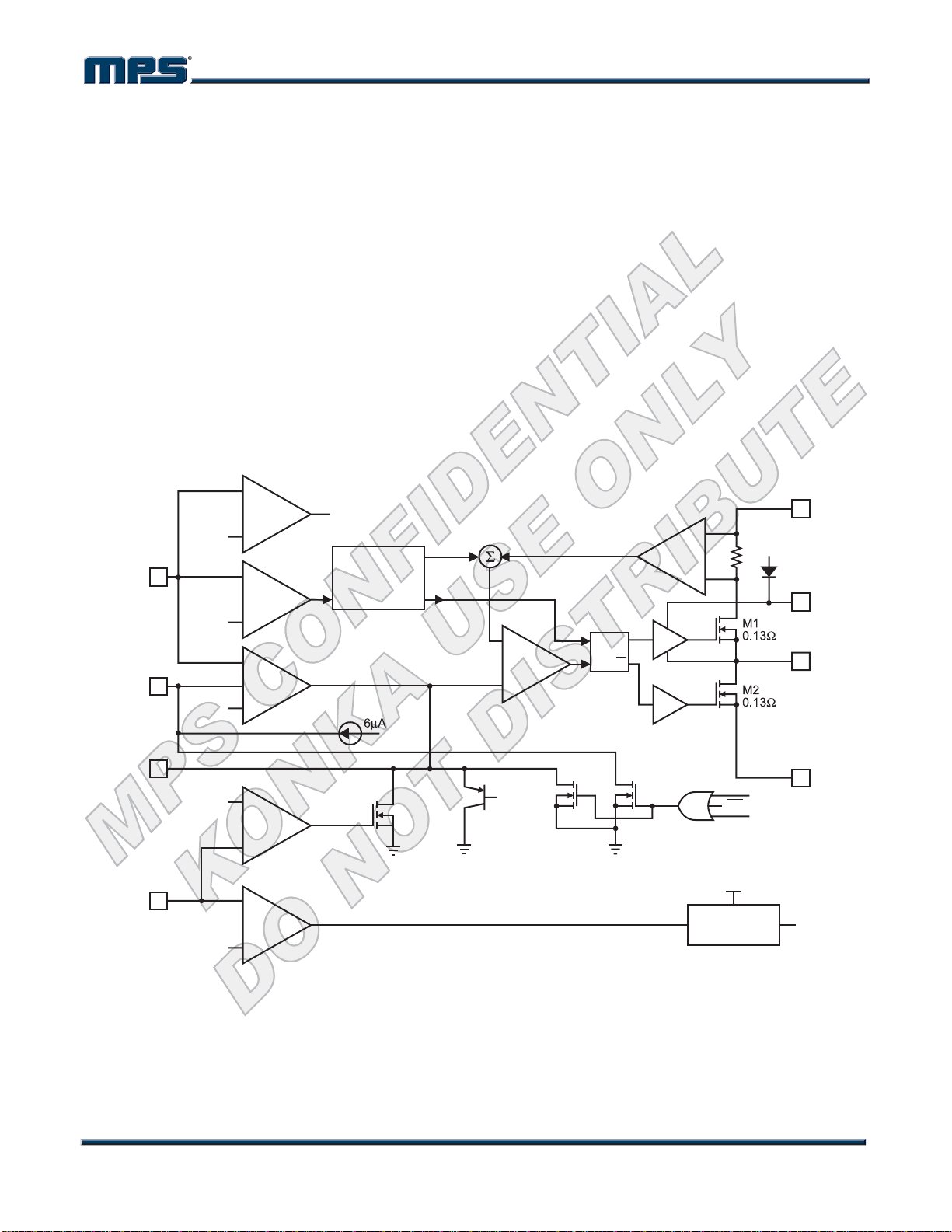
OPERATION
FUNCTIONAL DESCRIPTION
The MP1482 is a synchronous rectified,
current-mode, step-down regulator. It regulates
input voltages from 4.75V to 18V down to an
output voltage as low as 0.923V, and supplies
up to 2A of load current.
The MP1482 uses current-mode control to
regulate the output voltage. The output voltage
is measured at FB through a resistive voltage
divider and amplified through the internal
transconductance error amplifier. The voltage at
the COMP pin is compared to the switch current
measured internally to control the output
voltage.
The converter uses internal N-Channel
MOSFET switches to step-down the input
voltage to the regulated output voltage. Since
the high side MOSFET requires a gate voltage
greater than the input voltage, a boost capacitor
connected between SW and BS is needed to
drive the high side gate. The boost capacitor is
charged from the internal 5V rail when SW is low.
When the MP1482 FB pin exceeds 20% of the
nominal regulation voltage of 0.923V, the over
voltage comparator is tripped and the COMP
pin and the SS pin are discharged to GND,
forcing the high-side switch off.
FB
SS
COMP
EN
+
OVP
1.1V
5
0.3V
8
0.923V
6
2.5V
7
1.5V
--
+
--
--
+
+
+
-COMPARATOR
+
-COMPARATOR
OSCILLATOR
100/340KHz
ERROR
AMPLIFIER
EN OK
LOCKOUT
SHUTDOWN
RAMP
CLK
--
+
1.2V
CURRENT
COMPARATOR
CURRENT
SENSE
AMPLIFIER
SRQ
Q
+
--
INTERNAL
REGULATORS
EN
IN
5V
OVP
IN < 4.10V
2
1
3
4
IN
BS
SW
GND
5V
Figure 1—Functional Block Diagram
MP1482 Rev. 1.0 www.MonolithicPower.com 5
12/13/2007 MPS Proprietary Information. Unauthorized Photocopy and Duplication Prohibited.
© 2007 MPS. All Rights Reserved.
Page 29

MP1482 – 2A, 18V SYNCHRONOUS RECTIFIED, STEP-DOWN CONVERTER
MPS CONFIDENTIAL AND PROPRIETARY INFORMATION- KONKA USE ONLY
APPLICATIONS INFORMATION
COMPONENT SELECTION
Setting the Output Voltage
The output voltage is set using a resistive
voltage divider from the output voltage to FB pin.
The voltage divider divides the output voltage
down to the feedback voltage by the ratio:
2R
VV
=
OUTFB
Where V
is the feedback voltage and V
FB
the output voltage.
Thus the output voltage is:
923.0V
OUT
×=
R2 can be as high as 100k, but a typical value
is 10k. Using the typical value for R2, R1 is
determined by:
−×= (k)
OUT
2R1R
+
is
OUT
2R1R
+
2R
)923.0V(83.101R
Choose an inductor that will not saturate under
the maximum inductor peak current. The peak
inductor current can be calculated by:
V
OUT
V
⎞
⎟
⎟
IN
⎠
Where I
V
+=
II
LOADLP
is the load current.
LOAD
OUT
S
⎛
⎜
−×
1
⎜
××
Lf2
⎝
The choice of which style inductor to use mainly
depends on the price vs. size requirements and
any EMI requirements.
Optional Schottky Diode
During the transition between high-side switch
and low-side switch, the body diode of the lowside power MOSFET conducts the inductor
current. The forward voltage of this body diode
is high. An optional Schottky diode may be
paralleled between the SW pin and GND pin to
improve overall efficiency. Table 1 lists example
Schottky diodes and their Manufacturers.
For example, for a 3.3V output voltage, R2 is
10k, and R1 is 26.1k.
Inductor
The inductor is required to supply constant
current to the output load while being driven by
the switched input voltage. A larger value
inductor will result in less ripple current that will
result in lower output ripple voltage. However,
the larger value inductor will have a larger
physical size, higher series resistance, and/or
lower saturation current. A good rule for
determining the inductance to use is to allow
the peak-to-peak ripple current in the inductor
to be approximately 30% of the maximum
switch current limit. Also, make sure that the
peak inductor current is below the maximum
switch current limit. The inductance value can
be calculated by:
V
OUT
=
L
Where V
input voltage, f
I
is the peak-to-peak inductor ripple current.
L
is the output voltage, VIN is the
OUT
is the switching frequency, and
S
⎛
⎜
−×
1
⎜
∆×
If
LS
⎝
⎞
V
OUT
⎟
⎟
V
IN
⎠
Table 1—Diode Selection Guide
Voltage/Current
Part Number
Rating
Vendor
B130 30V, 1A Diodes, Inc.
SK13 30V, 1A Diodes, Inc.
MBRS130 30V, 1A International
Rectifier
Input Capacitor
The input current to the step-down converter is
discontinuous, therefore a capacitor is required
to supply the AC current to the step-down
converter while maintaining the DC input
voltage. Use low ESR capacitors for the best
performance. Ceramic capacitors are preferred,
but tantalum or low-ESR electrolytic capacitors
may also suffice.
Choose X5R or X7R
dielectrics when using ceramic capacitors.
Since the input capacitor (C1) absorbs the input
switching current it requires an adequate ripple
current rating. The RMS current in the input
capacitor can be estimated by:
V
OUT
V
⎞
⎟
⎟
IN
⎠
⎛
V
OUT
⎜
×
−×=
II
LOAD1C
1
⎜
V
IN
⎝
MP1482 Rev. 1.0 www.MonolithicPower.com 6
12/13/2007 MPS Proprietary Information. Unauthorized Photocopy and Duplication Prohibited.
© 2007 MPS. All Rights Reserved.
Page 30

MP1482 – 2A, 18V SYNCHRONOUS RECTIFIED, STEP-DOWN CONVERTER
MPS CONFIDENTIAL AND PROPRIETARY INFORMATION- KONKA USE ONLY
The worst-case condition occurs at VIN = 2V
where I
C1
= I
/2. For simplification, choose
LOAD
OUT
,
the input capacitor whose RMS current rating
greater than half of the maximum load current.
The input capacitor can be electrolytic, tantalum
or ceramic. When using electrolytic or tantalum
capacitors, a small, high quality ceramic
capacitor, i.e. 0.1µF, should be placed as close
to the IC as possible. When using ceramic
capacitors, make sure that they have enough
capacitance to provide sufficient charge to
prevent excessive voltage ripple at input. The
input voltage ripple for low ESR capacitors can
be estimated by:
OUT
V
⎛
⎜
1
−××
⎜
IN
⎝
I
LOAD
V
=∆
IN
V
f1C
×
S
V
OUT
V
IN
⎞
⎟
⎟
⎠
Where C1 is the input capacitance value.
Output Capacitor
The output capacitor is required to maintain the
DC output voltage. Ceramic, tantalum, or low
ESR electrolytic capacitors are recommended.
Low ESR capacitors are preferred to keep the
output voltage ripple low. The output voltage
ripple can be estimated by:
OUT
×
⎛
⎜
−×
1
⎜
Lf
⎝
OUT
S
V
=∆
V
V
OUT
V
⎞
⎜
⎟
⎟
⎜
IN
⎠
⎝
+×
R
ESR
⎛
⎞
1
⎟
⎟
××
2Cf8
S
⎠
Where C2 is the output capacitance value and
is the equivalent series resistance (ESR)
R
ESR
value of the output capacitor.
In the case of ceramic capacitors, the
impedance at the switching frequency is
dominated by the capacitance. The output
voltage ripple is mainly caused by the
capacitance. For simplification, the output
voltage ripple can be estimated by:
V
OUT
V
=
OUT
2
S
⎛
⎜
−×
1
⎜
×××
2CLf8
⎝
V
OUT
V
⎞
⎟
⎟
IN
⎠
In the case of tantalum or electrolytic capacitors,
the ESR dominates the impedance at the
switching frequency. For simplification, the
output ripple can be approximated to:
V
V ×⎟⎟
OUT
OUT
=
Lf
×
S
V
OUT
V
⎞
IN
⎠
R
ESR
⎛
1
⎜
−×
⎜
⎝
The characteristics of the output capacitor also
affect the stability of the regulation system. The
MP1482 can be optimized for a wide range of
capacitance and ESR values.
Compensation Components
MP1482 employs current mode control for easy
compensation and fast transient response. The
system stability and transient response are
controlled through the COMP pin. COMP pin is
the output of the internal transconductance
error amplifier. A series capacitor-resistor
combination sets a pole-zero combination to
control the characteristics of the control system.
The DC gain of the voltage feedback loop is
given by:
V
AGRA ×××=
EACSLOADVDC
Where A
G
is the current sense transconductance and
CS
R
is the load resistor value.
LOAD
is the error amplifier voltage gain;
VEA
FB
V
OUT
The system has two poles of importance. One
is due to the compensation capacitor (C3) and
the output resistor of the error amplifier, and the
other is due to the output capacitor and the load
resistor. These poles are located at:
G
Where G
f
=
1P
f
=
2P
is the error amplifier transconductance.
EA
EA
××π
1
××π
A3C2
R2C2
VEA
LOAD
The system has one zero of importance, due to the
compensation capacitor (C3) and the compensation
resistor (R3). This zero is located at:
f
=
1Z
1
3R3C2
××π
The system may have another zero of
importance, if the output capacitor has a large
capacitance and/or a high ESR value. The zero,
due to the ESR and capacitance of the output
capacitor, is located at:
f
ESR
=
1
××π
R2C2
ESR
MP1482 Rev. 1.0 www.MonolithicPower.com 7
12/13/2007 MPS Proprietary Information. Unauthorized Photocopy and Duplication Prohibited.
© 2007 MPS. All Rights Reserved.
Page 31

MP1482 – 2A, 18V SYNCHRONOUS RECTIFIED, STEP-DOWN CONVERTER
MPS CONFIDENTIAL AND PROPRIETARY INFORMATION- KONKA USE ONLY
In this case (as shown in Figure 2), a third pole
set by the compensation capacitor (C6) and the
compensation resistor (R3) is used to
compensate the effect of the ESR zero on the
loop gain. This pole is located at:
f
=
3P
1
3R6C2
××π
The goal of compensation design is to shape
the converter transfer function to get a desired
loop gain. The system crossover frequency
where the feedback loop has the unity gain is
important. Lower crossover frequencies result
in slower line and load transient responses,
while higher crossover frequencies could cause
system instability. A good rule of thumb is to set
the crossover frequency below one-tenth of the
switching frequency.
To optimize the compensation components, the
following procedure can be used.
1. Choose the compensation resistor (R3) to set
the desired crossover frequency.
Determine the R3 value by the following
equation:
V
V
f2C2
3R ×
=
××π
GG
×
CSEA
OUT
C
<×
V
FB
×
f1.02C2
×××π
GG
CSEA
OUT
S
V
FB
Where fC is the desired crossover frequency
which is typically below one tenth of the
switching frequency.
2. Choose the compensation capacitor (C3) to
achieve the desired phase margin. For
applications with typical inductor values, setting
the compensation zero, f
, below one-forth of
Z1
the crossover frequency provides sufficient
phase margin.
Determine the C3 value by the following equation:
3C
>
4
f3R2
××π
C
3. Determine if the second compensation
capacitor (C6) is required. It is required if the
ESR zero of the output capacitor is located at
less than half of the switching frequency, or the
following relationship is valid:
ESR
f
S
<
2
1
××π
R2C2
If this is the case, then add the second
compensation capacitor (C6) to set the pole f
P3
at the location of the ESR zero. Determine the
C6 value by the equation:
R2C
×
6C
=
ESR
3R
External Bootstrap Diode
An external bootstrap diode may enhance the
efficiency of the regulator, the applicable
conditions of external BST diode are:
z V
z Duty cycle is high: D=
=5V or 3.3V; and
OUT
V
OUT
>65%
V
IN
In these cases, an external BST diode is
recommended from the output of the voltage
regulator to BST pin, as shown in Fig.2
External BST Diode
BST
MP1482
SW
IN4148
C
BST
5V or 3.3V
+
L
C
OUT
Figure 2—Add Optional External Bootstrap
Diode to Enhance Efficiency
The recommended external BST diode is
IN4148, and the BST cap is 0.1~1µF.
Where R3 is the compensation resistor.
MP1482 Rev. 1.0 www.MonolithicPower.com 8
12/13/2007 MPS Proprietary Information. Unauthorized Photocopy and Duplication Prohibited.
© 2007 MPS. All Rights Reserved.
Page 32

MP1482 – 2A, 18V SYNCHRONOUS RECTIFIED, STEP-DOWN CONVERTER
MPS CONFIDENTIAL AND PROPRIETARY INFORMATION- KONKA USE ONLY
TYPICAL APPLICATION CIRCUIT
INPUT
7
EN
8
Figure 3—MP1482 with 3.3V Output, 22µF/6.3V Ceramic Output Capacitor
MP1482
SS
GND COMP
C6
(optional)
BSIN
12
SW
FB
64
C3
3.3nF
C5
10nF
3
5
D1
B130
(optional)
OUTPUT
3.3V
2A
MP1482 Rev. 1.0 www.MonolithicPower.com 9
12/13/2007 MPS Proprietary Information. Unauthorized Photocopy and Duplication Prohibited.
© 2007 MPS. All Rights Reserved.
Page 33

MP1482 – 2A, 18V SYNCHRONOUS RECTIFIED, STEP-DOWN CONVERTER
MPS CONFIDENTIAL AND PROPRIETARY INFORMATION- KONKA USE ONLY
PACKAGE INFORMATION
SOIC8
NOTICE: The information in this document is subject to change without notice. Please contact MPS for current specifications.
Users should warrant and guarantee that third party Intellectual Property rights are not infringed upon when integrating MPS
products into any application. MPS will not assume any legal responsibility for any said applications.
MP1482 Rev. 1.0 www.MonolithicPower.com 10
12/13/2007 MPS Proprietary Information. Unauthorized Photocopy and Duplication Prohibited.
© 2007 MPS. All Rights Reserved.
Page 34

CVMV26L
CVMV26L
Common Problems Solution
Common Problems Solution
-
A
-
A
-
-
4
4
0
0
—
—
—
—
—
—
—
—
System chart
System chart
Power Unit Problem Solving
Power Unit Problem Solving
Display Unit Problem Solving
Display Unit Problem Solving
Audio Unit Problem Solving
Audio Unit Problem Solving
—
—
Function Unit Problem Solving
Function Unit Problem Solving
Page 35

In stand-by condition,
Check the pin 1 of J3,
Whether have 12V?
N
N
Y
Main board testing point TP1 got 5V?TP6 got
3.3V?
Y
Check external
power
Check U7 and U5
Normal boot
power network
After power on, check the
pin 8 of U1 got 5V, testing
pin 3 of Q11 got 12V, testing
point TP4 got 3.3V
YN
Picture 1
Picture 1
Powe
Powe
r Unit P
r Unit P
roblem Solvin
roblem Solvin
g
g
(Q2、Q3) is burnt -out
OK
or loading is
shortcircuit, (Q11、
Q9) is burnt -out or
loading is shortcircuit,
power chip LDO(U4)is
running or not?
Page 36

Picture 2
Display unit(mess)
Mess or black screen
(back light on)
Whether driven board cable
is correct?
connection is Ok?
Y
N
Check whether it is OK
after chaning LCD?
N
Check output network,
Whether J2 driven board
socket part is normal?
Y
Whether the software
matches?
N
Repair this circuit
N
Change LCD
Y
Check whether
U8(TSUMV26)
power supply and
clock circuit chip LVDS
output pin
Upgrade the
matched software again
Check whether
Change
LCDpower VCC-Panel
driven board wire
is correct?J3 selects
correctly?Q14 output
voltage correctly?
is shortcircuit or
open circuit?
Page 37

Picture three
Display unit(black screen)
Black screen
of main board J5 got 12V?
Y
Whether the output voltage
Whether pin 5,6
N
for pin 4 of J5 is above 3.3V?
NY
Check and repair
power supply
Check and repair
Inverter is broken
power circuit
or connecting line is bad
Page 38

N
No sound
Picture 4
Whether there is any audio signal input or
Audio unit(no sound)
Whether amplifier power supply is normal?
Y
Whether the volume,
Y
MUTE
setting is normal?
YN
Whether there is
signal
output from J6?
N
Y
Whether there is signal
input in U9(YD1517P)1/9?
N
Check
peripheral
audio
equipment:
amplifier
power
supply
Resetting
Check
external
loudspeaker
Check and repair
amplifier
power supply
circuit ,
if power supply
is normal,
N
Check an d
repair U8
Check whether there is signal
output from U8audio output pin?
Y
Check and repair
network
of the connecting
part between U8
and U9
circuit
then change U9
Page 39

TV no searching
/no image
Picture 5
N
Check whether external RF
input signalis normal?
Function unit (ATV video broke down)
Y
Check whether
pin 7 of tuner U12 got 5V?
Y
Y
Check pin4,5of tuner U12,
whether there is I
Y
Whether there is intermediate-frequency signal
in pin 11 of U12?
N
2
C data?
N
N
Check whether the direct
connecting network for
U12/U11 is normal?
NY
Whether the
peripheral circuit of U12
is normal?
Y
N
Check whether
Check and
repair
peripheral
RF
equipment
Check video
sound meter U11
circuit and
U8(TSUMV26)
connecting
network
Repair this
connecting
circuit
Change
tuner
Check and
I2C network
Repair
repair power
pull-up voltage
this
supply
is normal?( pin 2
peripheral
network and
of R2 or pin 2 of
circuit
U6 circuit of
R7)
this pin
Page 40

TV no sound, only picture
Whether there is
sound under PC AV?
Picture 6
Function unit (ATV no sound
N
Y
Check U11 and it circuit
is normal
Y
N
Refer to
“NO SOUND”
repair guide
Change tuner
Repair this
circuit
Page 41

Under PC
Picture 8
Function unit(PC)
Image not
in the middle
Miss color,
Color
cast
Whether U8( TSUMV26)
R.G.B input signal is normal?
Whether the contact
of VGA socket is good?
Whether VS,HS signal
Image
No signal
shakes
Whether the
is regular or stable?
contact of
YN
YN
OSD setting
VGA socket
is good?
Carry out
auto-adjust
operation
The system
setting
is incorrect,
reset it
Check VGA
input circuit
doesn’t match,
reset it,
or input mode
doesn’t support
Check VS.HS
circuit
Check VS.HS
circuit
Page 42

Picture 9
Function unit(SCART,VGA)
RGB、SCART
SCART
miss color,
color cast
Whether U8( TSUMV26 )R.G.B
input signal is normal?
All has
no signal
YN
Whether the contact
of SCART socket
is good?
System setting
is incorrect,
reset it
Check SCART R.G.B
input network
Check
U8
( TSUMV26 )
power supply
Page 43

Picture 10
Function unit(HDMI)
Under HDMI
No image
HDMI related
network of U8(
Whether HDMI
There is image
contact is good?
but no sound
Whether there is
Y
TSUMV26 )
N
Y
sound under PC?
N
Refer to
"power failure"
repair flow
Check
HDMI input
network
Refer to "no
Check HDMI
sound"
input network
repair flow
Page 44

Picture 12
Function unit(YPBPR
)
YPBPR
YPBPR
miss color
or color cast
No signal
Check perpheral circuit,
Check Y/PB/PR
signal input network
crystal oscillator circui t
of U8
and input network
 Loading...