

Page 1
SERVICE MANUAL
DOCUMENTATION TECHNIQUE
TECHNISCHE DOKUMENTATION
DOCUMENTAZIONE TECNICA
DOCUMENTACION TECNICA
No copying, translation, modification on other use authorized. All rights reserved worldwide. • Tous droits de reproduction, de traduction, d'adaptation et d'exécution réservés pour tous les pays. • Sämtliche Urheberrechte an diesen Texten und Zeichnungen stehen uns zu. Nachdrucke,
Vervielfältigungen - auch auszugsweise - nur mit unserer vorherigen Zustimmung zulässig. Alle Rechte vorbehalten. • I diritti di riproduzione, di traduzione, e esecuzione sono riservati per tutti i paesi. • Derechos de reproduccion, de traduccion, de adaptacion y de ejecucion reservados para todos los paises.
WARNING : Before servicing this chassis please read the safety recommendations.
ATTENTION : Avant toute intervention sur ce châssis, lire les recommandations de sécurité.
ACHTUNG : Vor jedem Eingriff auf diesem Chassis, die Sicherheitsvorschriften lesen.
ATTENZIONE : Prima di intervenire sullo chassis, leggere le norme di sicurezza.
IMPORTANTE : Antes de cualquier intervención, leer las recomendaciones de seguridad.
- 0602
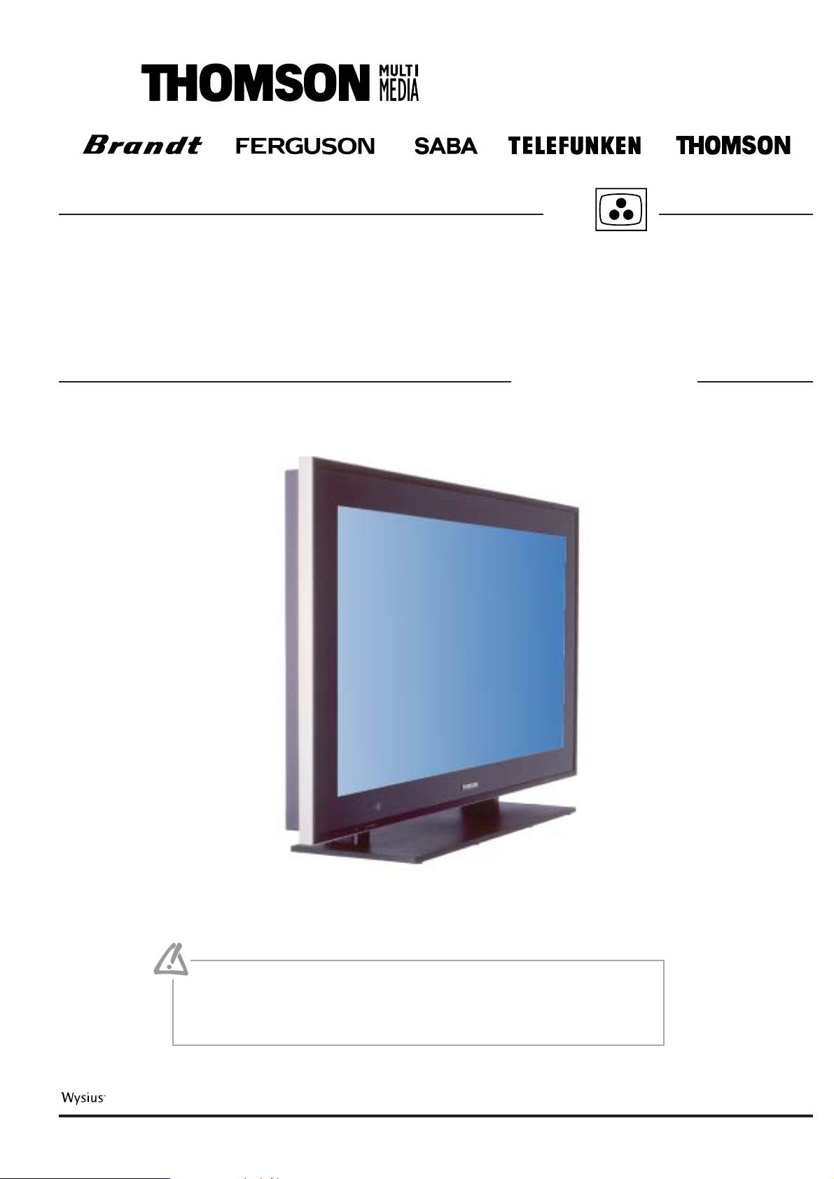
50WS94E
TV
Plasma
Page 2
Indicates critical safety components, and identical components should be used for replacement. Only then can the
operational safety be garanteed.
Le remplacement des éléments de sécurité (repérés avec le symbole ) par des composants non homologués selon la
Norme CEI 65 entraine la non-conformité de l'appareil. Dans ce cas, la responsabilité du fabricant n'est plus engagée.
Wenn Sicherheitsteile (mit dem Symbol gekennzeichnet) nicht durch Original - Ersatzteile ersetzt werden, erlischt die
Haftung des Herstellers.
La sostituzione dei componenti di sicurezza (evidenziati con il segno ) con componenti non omologati secondo la
norma CEI 65 comporta la non conformitá dell'apparecchio. In tal caso è "esclusa la responsabilità " del costruttore.
La sustitución de elementos de seguridad (marcados con el simbolo ) por componentes no homologados segun la
norma CEI 65, provoca la no conformidad del aparato. En ese caso, el fabricante cesa de ser responsable.
MEASUREMENT CONDITIONS - CONDITIONS DE MESURES - MESSBEDINGUNGEN
CONDIZIONI DI MISURA - CONDICIONES DE MEDIDAS
RICEVITORE :
In UHF, livello d'entrata 1 mV, monoscopio barre :
- PAL, norma G. bianco 100%.
Via SCART, livello d'entrata 1 Vpp, monoscopio barre :
Colore, Contrasto, Luminositá media, Suono minimo.
Programma selezionato PR 01.
Tensioni continue rilevate rispetto alla massa con un voltmetro digitale.
RECEIVER :
On UHF,input level : 1 mV, bar test pattern :
- PAL, I standard, 100% white.
Via the scart socket, input level : 1 Vpp, bar test pattern :
Colour, contrast and brightness at mid-position, sound at minimum.
Programme selected : PR 01.
DC voltages measured between the point and earth using a digital
voltmeter.
EMPFÄNGER :
Bei UHF Eingangspegel 1 mV, Farbbalken :
- PAL, Norm G, Weiss 100%.
Über die Scartbuchse : Eingangspegel 1 Vss, Farbbalken :
Farbe, Kontrast, Helligkeit in der Mitte des Bereichs, Ton auf Minimum.
Zugeordnetes Programm PR 01.
Gleichspannungen mit einem digitalen Voltmeter zur Masse gemessen.
RECEPTEUR :
En UHF, niveau d'entrée 1 mV mire de barres
- SECAM, Norm L, Blanc 100%.
Par la prise Péritélévision, niveau d'entrée 1 Vcc, mire de barres .
Couleur, contraste, lumière à mi-course, son minimum.
Programme affecté PR 01.
Tensions continues relevées par rapport à la masse avec un
voltmètre numérique.
RECEPTOR :
En UHF, nivel de entrada 1 mV, mira de barras :
- PAL, norma G, blanco 100%.
Por la toma Peritelevision, nivel de entrada 1 Vpp mira de barra.
Color, Contraste, luz a mitad de carrera, Sonido minimo.
Programa afectado PR 01.
Tensiones continuas marcadas en relacion a la masa con un voltimetro digital.
Do not disconnect modules when they are energized!
Repairs on power supply section are to be carried out only with isolating transformer.
Ne pas retirer les modules lorsqu' ils sont sous tension. N'effectuer les travaux de maintenance sur la partie reliée
au secteur (Switch Mode) qu'au travers d'un transformateur d'isolement.
Module nicht bei eingeschaltetem Gerät entfernen!
Servicearbeiten am Netzteil nur unter Verwendung eines Regeltrenntrafos durchführen.
Non scollegare le piastre quando sono alimentate!
Per le riparazioni sulla sezione alimentatore, utilizzare un trasformatore isolatore.
No desconectar los módulos cuando están activados. Las reparaciones en la sección de alimentación de energía
deben ser ejecutadas solamente con un transformador de separación.
Page 3

First issue 06 / 02 3
Page Page
DISASSEMBLY
Removing the back panel . . . . . . . . . . . . . . . . . . . 4
Removing the module assembly . . . . . . . . . . . . . . 5
Removing the PDP module . . . . . . . . . . . . . . . . . . 7
WIRE LOCATION . . . . . . . . . . . . . . . . . . . . . . . . . . . . . 7
DIAGNOSTIC . . . . . . . . . . . . . . . . . . . . . . . . . . . . . . . . . 9
VIDEO TROUBLESHOOTING
No picture . . . . . . . . . . . . . . . . . . . . . . . . . . . . . .14
No RGB signal . . . . . . . . . . . . . . . . . . . . . . . . . . .15
No HD/DVD picture . . . . . . . . . . . . . . . . . . . . . . .15
No still pictures of PC . . . . . . . . . . . . . . . . . . . . .16
No interlace motion picture . . . . . . . . . . . . . . . . .16
No progressive motion picture . . . . . . . . . . . . . .16
ADJUSTMENT . . . . . . . . . . . . . . . . . . . . . . . . . . . . . . 17
Power . . . . . . . . . . . . . . . . . . . . . . . . . . . . . . . . .18
Video screen position . . . . . . . . . . . . . . . . . . . . . 18
DVD/HD/DTV screen position . . . . . . . . . . . . . . . 18
RGB/PC signal timing table . . . . . . . . . . . . . . . . . 19
ADJUSTMENT LOCATION
MAIN module . . . . . . . . . . . . . . . . . . . . . . . . . . . . 27
VIDEO module . . . . . . . . . . . . . . . . . . . . . . . . . . 28
POWER module . . . . . . . . . . . . . . . . . . . . . . . . . 29
SUB module . . . . . . . . . . . . . . . . . . . . . . . . . . . . 29
BLOCK DIAGRAMS
MAIN module . . . . . . . . . . . . . . . . . . . . . . . . . . . . 30
VIDEO module . . . . . . . . . . . . . . . . . . . . . . . . . . 31
WIRING DIAGRAM . . . . . . . . . . . . . . . . . . . . . . . . . . 32
CONTENTS
Page 4
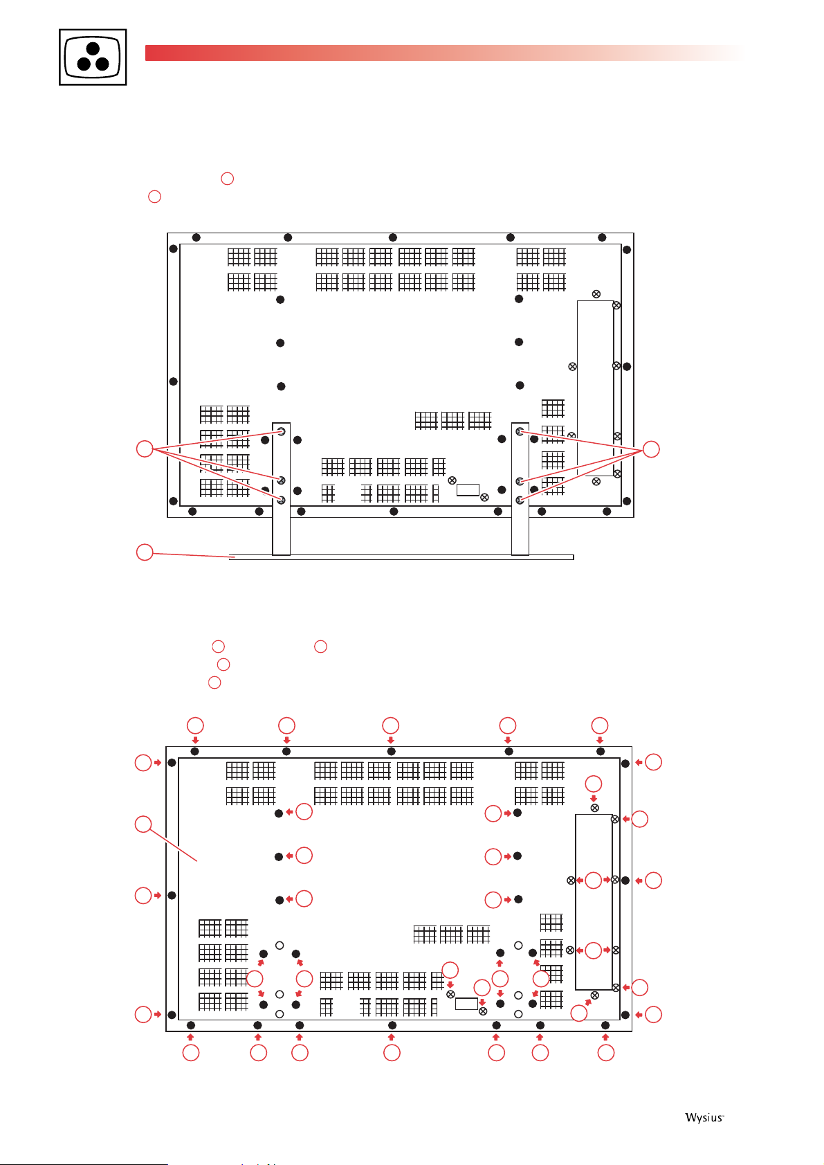
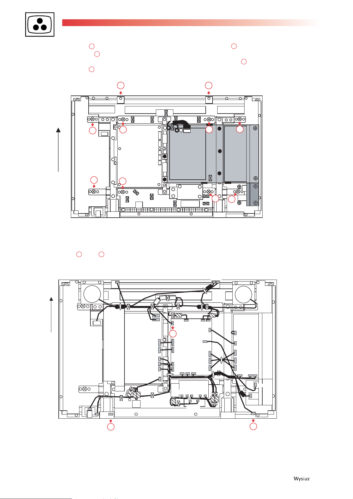
DISASSEMBLY
1. Removing the back panel assembly
- Remove the 6 screws and take out the foot holder
assembly ,
- Remove the 32 screws and the 2 screws ,
- Unscrew the 8 screws around the audio/video output
and lift the back cover up.
05
04
030206
01
4 First issue 06 /02
Fig. 1-1
Fig. 1-2
01
06
02 02 02 02 02
02
02
05
02
01
02
04
04
02
02
02
02
02
04
02
04
02
02
03
03
02 02
0202
04
04
02 02 02 02 02 02 02
Page 5
First issue 06 / 02 5
2. Removing the module assembly
- Remove the 2 screws and lift the bracket up,
- Unscrew the 8 screws and remove the shield cover ,
- Remove the 2 screws and the metal bracket,
- Unscrew the 8 screws , disconnect F2 (see fig. 2-4)
and remove the fans,
- Remove the 12 screws ,
14
1312111009
08
07
Fig. 2-1
Fig. 2-2
1007
TOP
12
14
20
14
09
09
07 08
2111
12
09
09
14
14
14
AD
19
TOP
14
11
1414
14
1414
14
Page 6
6 First issue 06 /02
- Remove the 8 screws ,
- Unscrew the 2 screws and remove the SENT/SENS
boards and brackets,
- Unscrew the screws and remove the ground terminal
(see fig. 2-2),
- Disconnect SW and LE connectors,
- Unscrew the screws and lift the ground terminal of AD
connector,
- Disconnect AD connector ,
192118
17
20
16
15
Fig. 2-4
Fig. 2-3
1616
15
15
TOP
15
15
T4
AD
15
15
T1 T2
15
15
PH
PD
TOP
PM
PN
PQ
PV
PA
PI
PW
LE
18
F2
13
PM
PN
LD
PW
AE SW RS
LM RM AB AE
AD F1 T1
SY
PL
BU
YU
PC
RM LM
DS
SY
BU
YU
PC
ABPVPQ
PL
RS
SW
17
Page 7

First issue 06 / 02 7
- Remove CN104 connector,
- Slightly lift the module assembly to disconnect CN105,
- Remove the module assembly
3. Removing the PDP module
- Remove the board assembly as explained in the previous
chapter,
- Unscrew the 4 screws at the corners of the PDP module,
- Remove the PDP module
Fig. 2-5
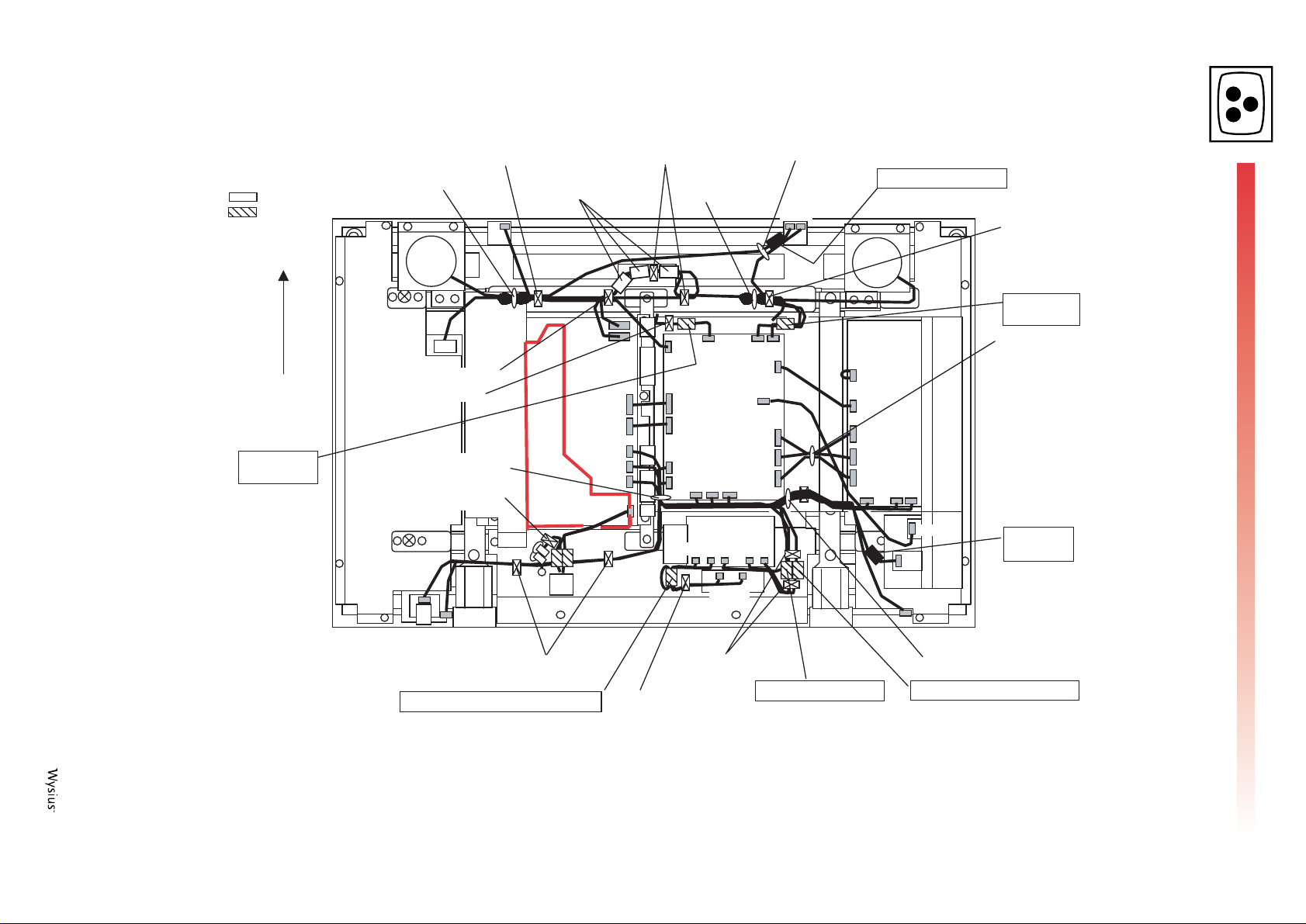
WIRE LOCATION
After replacement of the modules insert the connectors as specified below and refer to the following diagram to mount ferrites.
• CN-AD
Module -> MAIN PWB (AD)
• Left fan cable
Fan -> MAIN PWB (F2)
• Right fan cable
Fan -> MAIN PWB (F1)
• CN-PM
MAIN PWB (PM) -> Power unit (PM)
• CN-PN
MAIN PWB (PN) -> Power unit (PN)
• CN-SY
MAIN PWB (SY) -> VIDEO PWB (SY)
• CN-BU
MAIN PWB (BU) -> VIDEO PWB (BU)
• CN-YU
MAIN PWB (YU) -> VIDEO PWB (YU)
• CN-PC
MAIN PWB (PC) -> VIDEO PWB (PC)
• CN-PL
MAIN PWB (PL) -> PANEL PWB (PL) (PL label side)
• CN-RS
MAIN PWB (RS) -> 232C PWB (RS)
• CN-AE
MAIN PWB (AE) -> AUDIO PWB (AE)
• CN-T1
SENS PWB (T2) -> MAIN PWB (T1)
• CN-SW
CTL PWB (SW) -> MAIN PWB (SW)
• CN-LD
LED PWB (LD) -> MAIN PWB (LD)
• CN-PW
PWR PWB (PW) -> MAIN PWB (PW)
• CN-T2
SENS PWB (T1) -> SENT PWB (T4)
• CN-PD
Module CN105 -> Power unit (PD)
• CN-PH
Module CN104 -> Power unit (PH)
• Inlet ASSY
Inlet ASSY -> Power unit (PI)
• CN-PA
Power unit (PA) -> AUDIO PWB (PA)
• CN-PQ
Power unit (PQ) -> VIDEO PWB (PQ)
• CN-PV
Power unit (PV) -> VIDEO PWB (PV)
• CN-AB
VIDEO PWB (AB) -> AUDIO PWB (AB)
• CN-DS
VIDEO PWB (DS)
• CN-LM
SP PWB (LM) -> AUDIO PWB (LM)
• CN-RM
SP PWB (RM) -> AUDIO PWB (RM)
CN104
TOP
CN105
Page 8
8 First issue 06 /02
Wire the connectors, mount the two types of ferrite cores, and bundle the wires by means of clampers, etc.
(Caution)
Ferrite cores 3 pcs.
8 pcs.
TOP
AD passed
through FL12
Fan and PD fixed to M05
FAN, PD, and PH fixed
AD fixed
PQ, PV, PA, LD, and PW
fixed to M05
Green wire fixed
PW
LD
FAN, PD, and T2 fixed
PD and PH passed
through FL20 to 22
T4
PH
PD
A14
PD and PH fixed
PM
PN
PQ
PV
PA
PI
Fan and PH fixed
to M05
F2
AD F1 T1
PM
PN
LD
PW
AE SW RS
LM RM AB AE
RM LM
T1 and T2 fixed to M05
T1 T2
SY
PL
BU
YU
PC
T2 passed through FL36
DS
SY
BU
YU
PC
ABPVPQ
PL
RS
SW
FAN, T1, and PH
fixed
T1 passed
through FL35
BU,YU, and PC
fixed to M05
RS passed
through FL6
LD and PW fixed
LM and RM assembled twice on FL33
AB, AE, and PA fixed
LM and RM fixed
PA passed through FL11
AB, PV, PQ, SW, and RS fixed to M05
AE passed through 2 pcs of FL5
Safety Cautions
Cables other than the PI must not enter the area of AC primary side (within the red lines; actual items in the white line) of the power unit A14.
.
Page 9
First issue 06 / 02 9
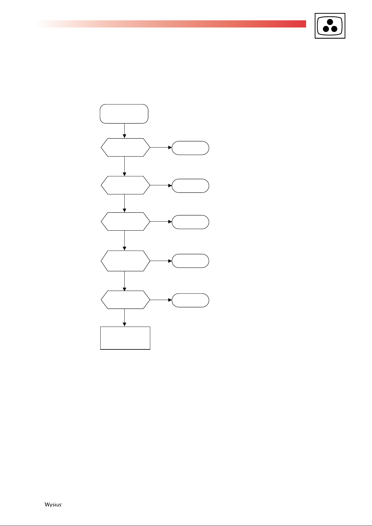
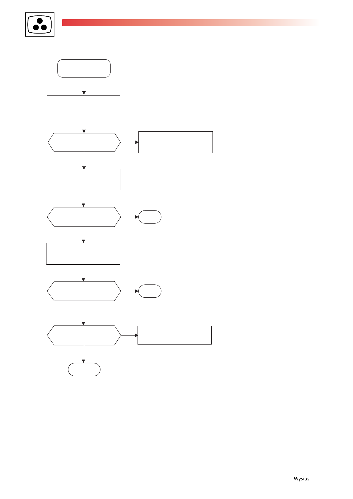
DIAGNOSTIC
The power LED located on the front of the display is a bicolour LED wich indicates the operating status including the normal, standby
and three error detections
No energization
of POWER unit
Is the power
LED lit ?
See page 10
Is the power LED
flashing green?
See page 11
Is the power LED
lighting green?
The power LED
is lighting red :
Stand-by mode
See page 13
Is the power LED
flashing red?
See page 10
Is the power
LED flashing green
and red?
See page 12
No
No
Yes
Yes
No
Yes
No
Yes
No
Yes
Page 10
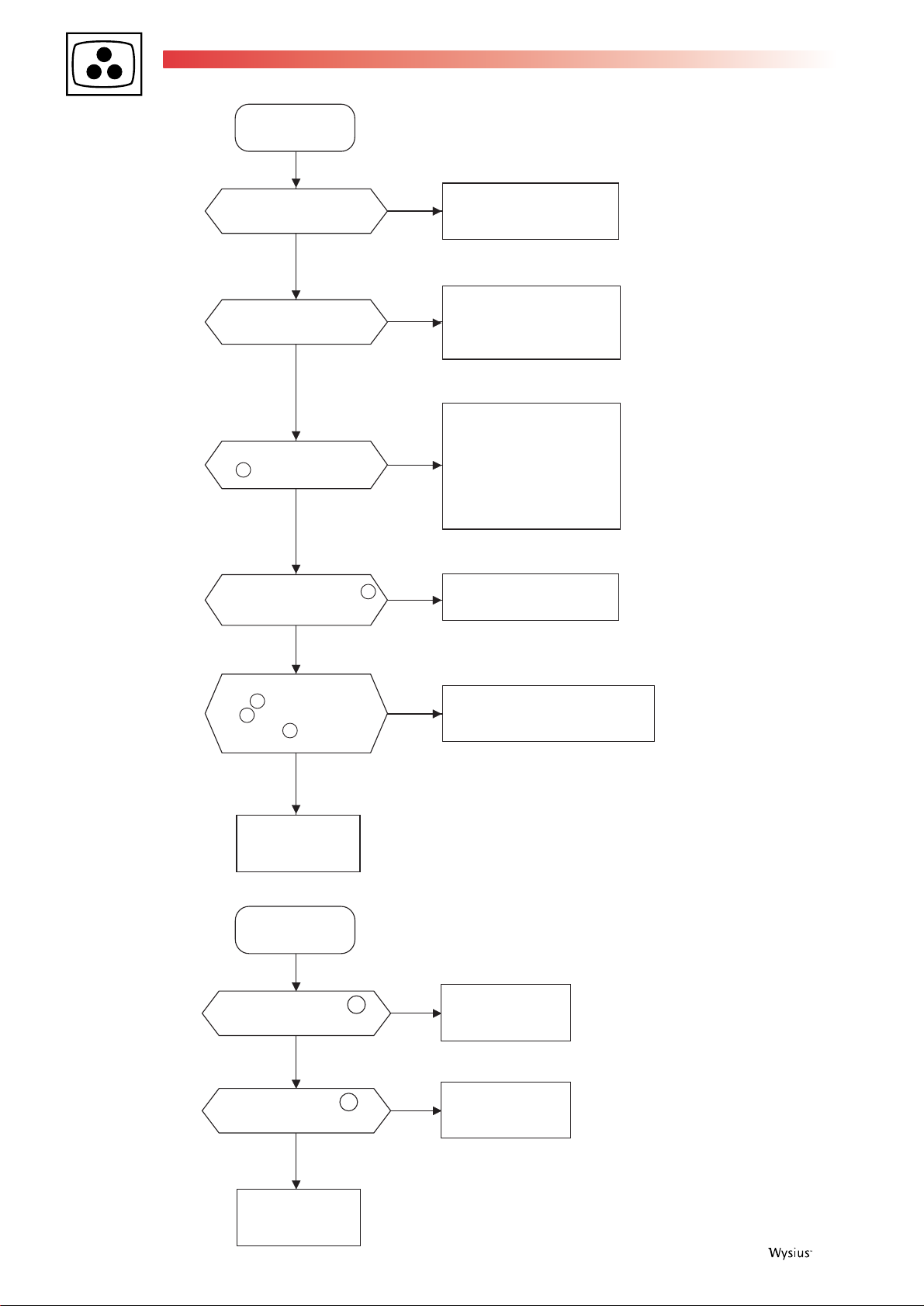
10 First issue 06 /02
Power LED
unlit
Is the power plug correctly
connected to the wall outlet?
Yes
Is there AC 100V behind
the fuses F1 and F2?
Yes
Is there M+7V output at
Pin 1 of the PM connector?
Yes
Is there +5V output at Pin 2
of IC9504 (MAIN module)?
Yes
No
No
No
No
Rearrange the power plug
connection correctly.
Fuses F1 and F2 have blown
out. Replace the fuses. If they
blow out again, the POWER
unit is out of order
Try to disconnect the PW, PQ,
and RS connectors from one
after another. If the output of
M+7V is available, the circuits
beyond these connectors are
out of order. If no output is
found, the POWER or the
MAIN unit is out of order.
Failure in the PWR module
Is there an output of +5V
at Pin 5 of the LD connector,
Pin 4 of the PW connector
and pin 5 of the RS
connector?
Yes
Failure in the
MAIN module
The power LED
is flashing red
Is 0V observed at Pin 10
of IC9806 (MAIN module)?
No
Is 5V observed at Pin 3 of
PN connector (MAIN module)?
No
Yes
Yes
Failure in +5V line. Check the LED,
PWR and RS232C modules
Failure in the
POWER unit
Failure in the
MAIN module
No
Failure in the
POWER unit
Page 11

First issue 06 / 02 11
The power LED
is flashing green
Does the fan run when
the main power circuit
is turned ON?
Yes
Connect a voltmeter to Pin
3 of F1 and F2 connectors
(MAIN module) and switch
the power ON
Is 5V available at Pin 3
of P0F1 and P0F2 connectors
(MAIN module)?
Yes
Is 5V available at Pin 3
of PN connectors
(MAIN module)?
Yes
No
No
No
Is 12V available at Pin 1 of
P0F1 and P0F2 connectors
(MAIN module)?
Yes
The fan is out of order on the
side where 5V is available
Failure in the POWER
module or in another IC
that uses A+5V line
No
Failure in the
MAIN module
Failure in the
MAIN module
Page 12

12 First issue 06 /02
The power LED is fla-
In the case of green and red flashing, the power supply
cannot be reset with the OFF/ON operation at the mains
power supply, remote control, and wall outlet.
For the alarm reset, keep pressing the input changeover key
of the main unit and move the mains power supply to the
"ON" position at the main unit. While doing so, it is
necessary to keep pressing the input changeover key of the
main unit for more than two seconds.In the case of green
and red flashing, the power supply cannot be reset with the
OFF/ON operation at the mains power supply, remote
control, and wall outlet.
shing red and green
Is 0V observed at Pin 100
of IC9501 (MAIN module)?
Yes
Is 0V observed at Pin 2 of
IC9505 (MAIN module)?
No
Is 5V observed at Pin 14 of
IC9505 (MAIN module)?
No
Is there +5V output at Pin 2
of IC9504 (MAIN module)?
Yes
Is there an output of +5V
at Pin 5 of the LD connector,
Pin 4 of the PW connector
and pin 5 of the RS
connector?
Yes
No
Yes
Yes
No
No
Failure in the
MAIN module
Failure in the
PDP module
Failure in the
MAIN module
Failure in the PWR module
Failure in +5V line. Check the LED,
PWR and RS232C modules
Failure in the
MAIN module
Page 13

First issue 06 / 02 13
The power LED
is lighting green
Switch the power ON
and listen to the
AC relay
Is it possible to hear the
AC relay switching ON?
Yes
Does the AC relay takes more
than 5 seconds to switch OFF,
after switching the power ON?
Yes
Is "H" maintained at Pin
3 of PM connector
(MAIN module)?
Yes
No
No
No
Is "H" maintained at
Pin 79 of IC9501
(MAIN module)?
Yes
Is "H" maintained at Pin
3 of PM connector
(MAIN module)?
Yes
Failure in the POWER module
Failure in the
MAIN module
No
No
Failure in the
MAIN module
Disconnect PM
connector
Is "H" maintained at Pin
1 of PD connector
(POWER module)?
Yes
Is the power supply built-up when
PD,PH and AD connectors are
disconnected (MAINmodule)?
Yes
Failure in the PDP
module or the
POWER unit
No
Failure in the
PDP module
Disconnect the PV, PQ, PN
and PA connectors one after
another (others kept connected)
and confirm that the power
No
supply is available. If it is not
available, the POWER unit is
out of order. Else, the circuit
of the disconnected connector
is out of order.
Is "H" maintained at Pin
3 of IC9501
(MAIN module)?
Yes
Failure in the
POWER unit
No
Failure in the
MAIN module
Page 14
14 First issue 06 /02
VIDEO TROUBLESHOOTING
No picture
Apply an NTSC grey scale
signal to the video input 1 cir-
cuit and select the video input 1
Is the on screen
display available
No
Replace AD, PD
and PH connector
No
Is the display normal?
No
Replace the MAIN module
Is the display normal?
No
Yes
Yes
Yes
Failure in the
MAIN module
End
End
Are the 170V, 70V and
D+5V signals availalble
on POWER module?
No
See page 9
Yes
Failure in the PDP module
Page 15

First issue 06 / 02 15
No video signal
at RGB input
Is RGB signal available at Pins
1 , 3 , 5 of the PC connector?
Yes
Are the H sync signals available
at Pins 7 and 10 and the V sync
signals available at Pins 9
and 12 of the PC connector?
Yes
Failure in the
MAIN module
No video signal at video
and HD/DVD inputs
No
No
Failure in the
VIDEO module
Failure in the
VIDEO module
Is YUV signal available at Pins
1 , 3 , 5 of the YU connector?
Yes
Are the H sync signals available
at Pins 7 and 10 and the V sync
signals available at Pins 9
and 12 of the YU connector?
Yes
Failure in the
MAIN module
No
No
Failure in the
VIDEO module
Failure in the
VIDEO module
Page 16

16 First issue 06 /02
No still pictures of
PC generated
No interlace motion
picture for video,
DVD and HDTV
No progressive motion
pictures generated
Apply a XGA 60 Hz grey
scale signal to the PC1
input circuit and select PC1
End
End
Apply a NTSC grey scale signal
to the video input circuit
and select video input 1
Replace AD connector cable
Yes
Yes
Is the display normal?
No
Replace YU connector cable
Is the display normal?
Apply a 525p grey scale signal
to the DVD1/HD1 input circuit
and select DVD1/HD1
No
Replace the MAIN module
Page 17

First issue 06 / 02 17
It could be necessary to change the zoom mode in order to
carry out some alignments of the set. Press the "format"
button of the remote control. The mode switches as shown in
the margin.
It is necessary to enter the Service Mode in order to carry out
alignment of the set. Most adjustments must be made with
the RCU.
• Using the remote control, press successively the zoom "-"
( -), exit, mute ( ) and zoom "-" ( -) buttons.
• The main service menu appears on the screen.
• Press the "menu" button to select the menu.
• Press the / buttons to select the menu line.
• Press the / buttons to make adjustments.
NB : the value of the adjustment is memorized automatically.
• To exit the service mode menu press successively, the
zoom "-" ( -), exit, mute ( ) and zoom "-" ( -) buttons
on the remote control.
• Enter the service mode and select the "usage time" menu,
• Using the remote control, press successively the mute
( ), , , and zoom "-" ( -) buttons.
ACCESSING SERVICE MODE
3
EXITING FROM SERVICE MODE
4
CLEARING THE USAGE TIME
2
NAVIGATION INSIDE THE SERVICE MODE
VE011
D CONTROL
NTSC
CONT -18
BRIGHT +15
U-COL 74
COLOR + 4
TINT -22
SERVICE MODE
Before entering the service mode, it could be necessary to
configure the plasma monitor in the On Screen menu.
• Using the remote control, press "menu" button.
• The "main" menu appears on the screen.
• Press the / buttons to select the "setup" line.
• The "setup" menu appears on the screen.
• Select the "color system" line.
• The "color system" menu appears on the screen.
• Press the / buttons to select the color standard.
1
ACCESSING COLOR STANDARD
MAIN MENU
OK SELECT EXIT
EXIT
PICTURE
SOUND
SCREEN
PREFERENCES
OPTIONS
SETUP
SETUP
OK SELECT RETURN
MENU
FREQUENCY
MENU LANGUAGE
COLOR SYSTEM
COLOR SYSTEM
RETURN
EXIT
COLOR SYSTEM
: 3.58NTSC
OK SELECT
OSD CONTROLS
ZOOM SEQUENCE
ADJUSTMENTS
ADJUSTMENTS NECESSARY AFTER REPLACEMENT OF MODULES:
- After replacement of MAIN module or Video module, perform the adjusments of "video screen position" and "DVD/HD/DTV
screen position".
- After replacement of POWER or PDP module , perform the adjusment of "+170V/+70V" and "+5V". When replacing PDP
module, also perform "screen position" adjustments and reset the "usage time" as shown below.
Replacing another module does not require further adjustment unless abnormal conditions are encountered.
zoom
4/3
16/9cinemarama
Page 18

18 First issue 06 /02
SERVICE
MODE
"POSITION"
menu
SERVICE
MODE
"POSITION"
menu
Video screen
position
MAIN
DVD/HD screen
position
MAIN
RV4
(D+170V ADJ)
RV3
(D+70V ADJ)
RV2
(D+5V ADJ)
POWER
+170V
+70V
POWER
+5V
NTSC test pattern :
HDTV test pattern :
Select VIDEO input with the
Remote Control or keyboard
Select "full screen" with the
"zoom" key of the Remote
Control
Check HD SELECT = 1035i
Select DVD/HD input with the
Remote Control or keyboard
Select "full screen" with the
"zoom" key of the Remote
Control
Video input
DVD/HD input
TP3
TP4
TP2
TP4
TP2/TP3
If there is any displacement of the display range in the PDP module, select
"MHPOS" and "MVPOS" lines, and adjust correctly.
If there is any displacement of the display range in the PDP module, select
"MHPOS" and "MVPOS" lines, and adjust correctly.
Select "H POS" line and adjust
Select "V POS" line and adjust
Check that "H PHA" = 0 and "H CLK" = 0
Adjust separate for cinema; 4/3; 16/9 and PAL.
Select "H POS" line and adjust
Select "V POS" line and adjust
Check that "H PHA" = 0 and "H CLK" = 0
Repeat adjustment for NTSC.
Adjust RV4 to obtain the specified PDP module
voltage value +/-1V at TP3 (+170V). This value is
indicated on the label pasted on the back of PDP module
Adjust RV2 :
V = 5.1 V +/- 0.1 V
Check that the voltage at TP2 and TP3 does not change.
If it changes, perform the previous adjustments again.
Adjust RV3 to obtain the specified PDP module
voltage value +/-1V at TP2 (+70V). This value is indicated
on the label pasted on the back of PDP module
DTV 1080i test pattern :
Check HD SELECT = 1080i
Select DVD/HD input with the
Remote Control or keyboard
Select "full screen" with the
"zoom" key of the Remote
Control
DVD/HD input
If there is any displacement of the display range in the PDP module, select
"MHPOS" and "MVPOS" lines, and adjust correctly.
Select "H POS" line and adjust
Select "V POS" line and adjust
Check that "H PHA" = 0 and "H CLK" = 0
Repeat adjustment for HD SELECT =1080B
DTV 720P test pattern :
Check HD SELECT = 1080i
Select DVD/HD input with the
Remote Control or keyboard
Select "full screen" with the
"zoom" key of the Remote
Control
DVD/HD input
If there is any displacement of the display range in the PDP module, select
"MHPOS" and "MVPOS" lines, and adjust correctly.
Select "H POS" line and adjust
Select "V POS" line and adjust
Check that "H PHA" = 0 and "H CLK" = 0
Repeat adjustment for DTV 480P
V=
V=
TP1
TP4
V=
Apply colour bar test pattern
to either Video, HD/DVD or
VGA input
Apply colour bar test pattern
to either Video, HD/DVD or
VGA input
Page 19

First issue 06 / 02 19
RGB/PC signal timing table:
PC mode 1 2 3 4 5
Signal name VU-6010 VU-6010 PC98 IBM PC98
NTSC PAL/SECAM 400@56Hz 400@70Hz 480@60HZ
Definition 640*240 768*288 640*400 640*400 640*480
Dot clock frequency (MHz) 12.214 14.752 21.053 25.175 25.175
H frequency (kHz) 15.734 15.557 24.826 31.469 31.469
V frequency (Hz) 59.94 50.39 56.423 70.086 59.94
H total (uS) 63.534 64.262 40.285 31.778 31.778
(dots) 776 948 848 800 800
H display period (uS) 52.4 52.06 30.4 25.422 25.422
(dots) 640 768 640 640 640
H front porch (uS) 1.146 1.288 2.803 0.675 0.596
(dots) 14 19 59 17 15
H sync pulse width (uS) 8.76 8.677 3.04 2.542 3.813
(dots) 107 128 64 64 96
H back porch (uS) 1.228 2.237 4.037 3.138 1.946
(dots) 15 33 85 79 49
V total (mS) 16.652 20.055 17.723 14.268 16.683
(line) 262 312 440 449 525
V display period (mS) 15.3 18.513 16.112 12.711 15.253
(line) 240 288 400 400 480
V front porch (mS) 0.191 0.321 0.282 0.413 0.191
(line) 3 5 7 13 6
V sync pulse width (mS) 1.144 1.093 0.322 0.064 0.064
(line) 18 17 8 2 2
V back porch (mS) 0.064 0.064 1.007 1.08 1.176
(line) 1 1 25 34 37
H sync polarity Neg Neg Neg Neg Neg
V sync polarity Neg Neg Neg Neg Neg
Scan type Interlaced Interlaced Non Non Non
Interlaced Interlaced Interlaced
VGROM NO. 1 2 3 4
5
Page 20

20 First issue 06 /02
PC mode 6 7 8 9 10
Signal name MAC@13Ó VESA VESA VESA XGA-2
480@72Hz 480@75Hz 480@85Hz 480@75HZ
Definition 640*480 640*480 640*480 640*480 640*480
Dot clock frequency (MHz) 30.24 31.5 31.5 36.0 31.5
H frequency (kHz) 35 37.861 37.5 43.269 39.375
V frequency (Hz) 66.667 72.809 75 85.008 75
H total (uS) 28.571 26.413 26.667 23.111 25.4
(dots) 864 832 840 832 800
H display period (uS) 21.164 20.317 20.317 17.778 20.32
(dots) 640 640 640 640 640
H front porch (uS) 2.116 0.762 0.508 1.556 0.508
(dots) 64 24 16 56 16
H sync pulse width (uS) 2.116 1.27 2.032 1.556 3.048
(dots) 64 40 64 56 96
H back porch (uS) 3.175 4.064 3.81 2.222 1.524
(dots) 96 128 120 80 48
V total (mS) 15 13.735 13.333 11.764 13.333
(line) 525 520 500 509 525
V display period (mS) 13.714 12.678 12.8 11.093 12.19
(line) 480 480 480 480 480
V front porch (mS) 0.086 0.237 0.027 0.023 0.279
(line) 3 9 1 1 11
V sync pulse width (mS) 0.086 0.079 0.08 0.069 0.051
(line) 3 3 3 3 2
V back porch (mS) 1.114 0.739 0.427 0.578 0.813
(line) 39 28 16 25 32
H sync polarity Sync on G Neg Neg Neg Neg
V sync polarity Sync on G Neg Neg Neg Neg
Scan type Non Non Non Non Non
Interlaced Interlaced Interlaced Interlaced Interlaced
VGROM NO. 6 7 8 9 1
0
Page 21

First issue 06 / 02 21
PC mode 11 12 13 14 15
Signal name VESA VESA VESA VESA VESA
600@56Hz 600@60Hz 600@72Hz 600@75Hz 600@85Hz
Definition 800*600 800*600 800*600 800*600 800*600
Dot clock frequency (MHz) 36 40 50 49.5 56.25
H frequency (kHz) 35.156 37.879 48.077 46.875 53.674
V frequency (Hz) 56.25 60.317 72.188 75 85.061
H total (uS) 28.444 26.4 20.8 21.333 18.631
(dots) 1024 1056 1040 1056 1048
H display period (uS) 22.222 20 16 16.162 14.222
(dots) 800 800 800 800 800
H front porch (uS) 0.667 1 1.12 0.323 0.569
(dots) 24 40 56 16 32
H sync pulse width (uS) 2 3.2 2.4 1.616 1.138
(dots) 72 128 120 80 64
H back porch (uS) 3.556 2.2 1.28 3.232 2.702
(dots) 128 88 64 160 152
V total (mS) 17.778 16.579 13.853 13.333 11.756
(line) 625 628 666 625 631
V display period (mS) 17.067 15.84 12.48 12.8 11.179
(line) 600 600 600 600 600
V front porch (mS) 0.028 0.026 0.77 0.021 0.019
(line) 1 1 37 1 1
V sync pulse width (mS) 0.057 0.106 0.125 0.064 0.056
(line) 2 4 6 3 3
V back porch (mS) 0.626 0.607 0.478 0.448 0.503
(line) 22 23 23 21 27
H sync polarity Pos. Pos. Pos. Pos. Pos.
V sync polarity Pos. Pos. Pos. Pos. Pos.
Scan type Non Non Non Non Non
Interlaced Interlaced Interlaced Interlaced Interlaced
VGROM NO. 11 12 13 14
15
Page 22

22 First issue 06 /02
PC mode 16 17 18 19 20
Signal name MAC@16Ó I/O dater CEREB VESA wide VESA wide
wide wide 1 (NEC 1) (NEC 2)
Definition 832*624 852*480 864*480 848*480 1024*576
Dot clock frequency (MHz) 57.2832 34.006 42.526 33.75 47.25
H frequency (kHz) 49.725 31.722 37.5 31.02 35.795
V frequency (Hz) 74.55 59.966 75 60 60.059
H total (uS) 20.111 31.524 26.667 32.237 27.937
(dots) 1152 1072 1134 1088 1320
H display period (uS) 14.524 25.055 20.317 25.126 21.672
(dots) 832 852 864 848 1024
H front porch (uS) 0.559 0.659 0.508 0.474 0.339
(dots) 32 22 22 16 16
H sync pulse width (uS) 1.117 3.764 2.032 3.319 3.048
(dots) 64 128 86 112 144
H back porch (uS) 3.91 2.047 3.81 3.319 2.878
(dots) 224 70 162 112 136
V total (mS) 13.414 16.676 13.333 16.667 16.65
(line) 667 529 500 517 596
V display period (mS) 12.549 15.132 12.8 15.474 16.091
(line) 624 480 480 480 576
V front porch (mS) 0.02 0.378 0.027 0.193 0.056
(line) 1 12 1 6 2
V sync pulse width (mS) 0.06 0.095 0.08 0.258 0.112
(line) 3 3 3 8 4
V back porch (mS) 0.784 1.072 0.427 0.741 0.391
(line) 39 34 16 23 14
H sync polarity Sync on G Neg Pos. Pos. Pos.
V sync polarity Sync on G Neg Neg Pos. Pos.
Scan type Non Non Non Non Non
Interlaced Interlaced Interlaced Interlaced Interlaced
VGROM NO. 16 17 18 19
20
Page 23

First issue 06 / 02 23
PC mode 21 22 23 24 25
Signal name VESA wide VESA wide CEREB VESA VESA
(NEC 3) (NEC 4) wide 2 768@60Hz 768@70Hz
Definition 1280*720 1360*765 1024*600 1024*768 1024*768
Dot clock frequency (MHz) 76.5 85.5 51.2 65 75
H frequency (kHz) 45.106 47.712 37.879 48.363 56.476
V frequency (Hz) 60.142 60.015 60.317 60.004 70.069
H total (uS) 22.17 20.959 26.4 20.677 17.707
(dots) 1696 1792 1352 1344 1328
H display period (uS) 16.732 15.906 20 15.754 13.653
(dots) 1280 1360 1024 1024 1024
H front porch (uS) 0.627 0.749 1 0.369 0.32
(dots) 48 64 51 24 24
H sync pulse width (uS) 2.301 2.058 3.2 2.092 1.813
(dots) 176 176 164 136 136
H back porch (uS) 2.51 2.246 2.2 2.462 1.92
(dots) 192 192 113 160 144
V total (mS) 16.627 16.662 15.579 16.666 14.272
(line) 750 795 628 806 806
V display period (mS) 15.962 16.034 15.84 15.88 13.599
(line) 720 765 600 768 768
V front porch (mS) 0.089 0.084 0.026 0.062 0.053
(line) 4 4 1 3 3
V sync pulse width (mS) 0.177 0.168 0.106 0.124 0.106
(line) 8 8 4 6 6
V back porch (mS) 0.399 0.377 0.607 0.6 0.513
(line) 18 18 23 29 29
H sync polarity Pos. Pos. Neg Neg. Neg.
V sync polarity Pos. Pos. Pos. Neg. Neg.
Scan type Non Non Non Non Non
Interlaced Interlaced Interlaced Interlaced Interlaced
VGROM NO. 21 22 23 24
25
Page 24

24 First issue 06 /02
PC mode 26 27 28 29 30
Signal name VESA VESA MAC@19Ó VESA VESA
768@75Hz 768@85Hz 1024@60Hz 1024@75Hz
Definition 1024*768 1024*768 1024*768 1280*1024 1280*1024
Dot clock frequency (MHz) 78.75 94.5 80 108 135
H frequency (kHz) 60.023 68.677 60.24 63.981 79.976
V frequency (Hz) 75.029 84.997 74.93 60.02 75.025
H total (uS) 16.66 14.561 16.600 15.63 12.501
(dots) 1312 1376 1328 1688 1688
H display period (uS) 13 10.836 12.8 11.852 9.481
(dots) 1024 1024 1024 1280 1280
H front porch (uS) 0.203 0.508 0.4 0.444 0.119
(dots) 16 48 32 48 2
H sync pulse width (uS) 1.219 1.016 1.2 1.037 1.067
(dots) 96 96 96 112 144
H back porch (uS) 2.235 2.201 2.2 2.296 1.837
(dots) 176 208 176 248 248
V total (mS) 13.328 11.765 13.347 16.661 13.329
(line) 800 808 804 1066 1066
V display period (mS) 12.795 11.183 12.749 16.005 12.804
(line) 768 768 768 1024 1024
V front porch (mS) 0.017 0.015 0.050 0.016 0.013
(line) 1 1 3 1 1
V sync pulse width (mS) 0.05 0.044 0.050 0.047 0.038
(line) 3 3 3 3 3
V back porch (mS) 0.466 0.524 0.498 0.594 0.475
(line) 28 36 30 38 38
H sync polarity Pos. Pos. Ñ Pos. Pos.
V sync polarity Pos. Pos. Ñ Pos. Pos.
Scan type Non Non Non Non Non
Interlaced Interlaced Interlaced Interlaced Interlaced
VGROM NO. 26 27 28 29
30
Page 25

First issue 06 / 02 25
PC mode 31 32 33 34 35
Signal name IDC-3000G IDC-3000G HDTV -J DTV (480P) DTV (720P)
PA L 625P NTSC 525P
Definition 768*576 640*480 1920*1034 644*483 1280*720
Dot clock frequency (MHz) 29.687 24.39 74.25 24.37 74.25
H frequency (kHz) 31.389 31.47 33.75 31.469 45.000
V frequency (Hz) 50 59.9 60/60 59.94 60
H total (uS) 31.933 31.775 29.63 31.777 22.222
(dots) 948 775 2200 774 1650
H display period (uS) 25.87 26.24 25.86 26.427 17.239
(dots) 768 640 1920 644 1280
H front porch (uS) 0.269 0.41 0.59 0.75 0.943
(dots) 8 10 44 18 70
H sync pulse width (uS) 2.526 2.46 0.59 2.35 1.077
(dots) 75 60 44 57 80
H back porch (uS) 3.267 2.665 2.59 2.25 2.963
(dots) 97 65 192 55 220
V total (mS) 19.911 16.522 16.652 16.683 16.667
(line) 625 525 562/562 525 750
V display period (mS) 18.35 15.106 15.319 15.348
(line) 576 480 517/517 483 720
V front porch (mS) 0.223 0.252 0.148 0.191 0.111
(line) 7 8 5 6 5
V sync pulse width (mS) 0.223 0.22 0.148 0.191 0.111
(line) 7 7 5 6 5
V back porch (mS) 1.115 0.944 1.037 0.953 0.444
(line) 35 30 35 30 20
H sync polarity Neg Neg Neg Neg Neg
V sync polarity Neg Neg Neg Neg Neg
Scan type Non Non Interlaced Non Non
Interlaced Iinterlaced Interlaced Interlaced
VGROM NO. 31 32 33 34
35
Page 26

26 First issue 06 /02
PC mode 36 37 38 39
Signal name HDTV -W SSPE JSPE MAC@12Ó
Definition 1920*1080 1024*512 852*480 1152*870
Dot clock frequency (MHz) 74.25 40 16 100
H frequency (kHz) 33.75 33.727 15.75 68.681
V frequency (Hz) 60/60 60.012 59.94 75.062
H total (uS) 29.630 29.650 63.750 14.560
(dots) 2200 1186 1020 1456
H display period (uS) 25.859 25.600 53.250 11.520
(dots) 1920 1024 852 1152
H front porch (uS) 0.593 0.600 1.250 0.320
(dots) 44 24 20 32
H sync pulse width (uS) 1.185 1.200 4.750 1.280
(dots) 88 48 76 128
H back porch (uS) 1.993 2.250 4.500 1.440
(dots) 148 90 72 144
V total (mS)
16.652/16.682
(line) 562/563 562 262.5/262.5 915
16.663 16.683 13.322
V display period (mS)
(line) 540/540 511 239/239 870
V front porch (mS) 0.059/0.074 0.178 0.064/0.096 0.044
(line) 2/2.5 6 1/1.5 3
V sync pulse width (mS) 0.148/0.148 0.148 0.191/0.191 0.044
(line) 5/5 5 3/3 3
V back porch (mS) 0.444/0.459 1.186 1.211/1.243 0.568
(line) 15/15.5 40 19/19.5 39
H sync polarity Neg Neg Neg Sync on G
V sync polarity Neg Neg Neg Sync on G
Scan type Interlaced Non Interlaced Non
VGROM NO. 36 37 38 39
16.000/16.000
15.15
Interlaced Interlaced
15.236/15.236
12.667
Page 27

First issue 06 / 02 27
ADJUSTMENT LOCATION
MAIN module
AD
SCREEN
PRE
100M
IC
6702
LVDS LVDS
IC
F2
T1
9802IC9803
FL
3.3V
FL
3.3V
D+5
M7
A14
A+5
IC
9502
OSD
RERE
POST
FLASH
AMDP2
SDRAM
RE
GGG
1.2.1.
852
IC
6502
ADC
(Y Pb Pr)
F1
ADC
(RGB)
SELECTERSELECTER
T1
SY
SDRAM
SDRAM
PANEL
LINK
PL
Pn
P
BUYUPC
CPU
EXT -PC
PW LD WR PN PM
RSSWAE
FILTER
(FOR
HDTV)
FILTER
(FOR VIDEO)
ANP
(YPbPr)
FILTER
(FOR PC)
AMP
(FOR PC)
Page 28

28 First issue 06 /02
VIDEO module
PL
PANEL LINK PWB
IC5314
IC5313
IC5316
IC5312
IC5302
IC5310
IC5306~
IC5303
IC5303
IC5001
VIDEO1
VIDEO2
VIDEO3
S Terminal
T2 T1
T3
35
DS
BU SY
IC5502
IC5505
IC5506
IC5501
IC5503
IC5504IC5852IC5856
IC5311
IC5510
IC5508
IC5509
IC5301
RGB1
D-SUB 15PIN
T8 T7 T6 T5 T4
SENV PWB SENU PWB SENT PWB SENS PWB
YUPC
IC5509IC5508
IC5868
IC5854
IC5851 IC5867 IC5869 IC5866
IC5701
PQPVAB
5BNC
RGB2/HD2/D VD2
AUDI03 AUDI02 HD1/D VD2 AUDI01
Page 29

First issue 06 / 02 29
POWER module
SUB module
PM PN PQ PV PA PI
PD
PH
TP3
D+170
RV4
D+170
ADJ
TP4
D. GND
TP2
D+70
TP1
D+5V
RV2
D+5 ADJ
RV3
D+70
ADJ
PWC-4419B
PWC-4419C
PWR PWB
LED PWB
PWC-4419D
PWC-4419E
SP PWB
CTL PWB
PWC-4419A 232CPWB
Page 30

30 First issue 06 /02
/
/
T
/f
VIDEO
PWB
p/
p/
BLOCK DIAGRAMS
MAIN module
set
FAN*2
REG*2
M62320
I/O expand
IC9501
OUTPUT LEVEL
MODULE(A/D INPUT)
POSYNC
POSYNC
PDADP
PDADY
SCL6/SDA6
SCL5/SDA5
SCL2/SDA2
SCL1/SDA1
SDA/SCL
System Controller CPU
POMUTE
POWER
XPLLRST
XRST/ENAMDP/
BLKMARI
VMUTE
SMUTE
SIK3/SID3
ENPDP
SDIN2
SIK2/SID2/RSTYUMA
CSYUMA
SDIN1
SIK1/SID1/RSTSCR
CSSCR
CSOSD
SMODE2/S2SW
SBMHD/SBMVD
SMODE1/S1SW
MNMHD/MNMVD
SCL4/SDA4
SCL3/SDA3
RXD/TXD
CONTROLE LOCK
REMIN
LEDCTL1/LEDCTL2
CTL1/CTL2
FAN
power supply
REG
ON/OFF
To ADC
SDA/SCL
To/from
rom
o
M62320
I/O expand
from MODULE
(5Vp-p)
PSS/ALARM
IC9502
E2P-ROM
POWER
To AMDP
To G/A
To PDP
To AUDIO
To PDP
To G/A
Ffom SCREEN
To OSD/SCREEN
To SCREEN
To OSD
assist
FAN*2
REG
ON/OFF
CAT24WC16
FAN OUT
POWER
SUPPLY
T-ALM1/2
POWER
To CPU
SIK2/SID2
SIK2/SID2
Analog video signal
Digital video signal(without VIDEO mode)
Digital video signal(VIDEO mode)
Single Line
(CPU)
Temp
POMUTE
To CPU
SDA5/SCL5
IC9004
Image Processor
G/A
SDIN2 /CSGA/RSTYUMA
SDA1/SCL1/ENAMDP/XRST/
XPLLRS from CPU
SDRAM
X'TAL
ICXXXX
SDIN2 /CSGA/RSTYUMA
PRE G/A
SDA6/SCL6
Two or more Lines
Sensor*2
uPDxxxxxxx
Matrix and Composer
IC7502
Flash ROM
5V 3V
ICXXXX
XXXXXXXXXX
10MHz
Matrix
de-Matrix
Image Processor
A/D
/PDADY
RGB
LFP
PLASMA
MODULE
from CPU
Matrix
48
IC7506
Digital
TMCxxxxx
Signal Processor
48bit
IC6XXX
Converter
IC6001,2,3,
Selector
SN74AHC2G66
10MHz
30MHz
PSC/PLE/ALARM/
BLKH
Timing
Generator
sysnc2/Sync3
Sync0/Sync1
CXA3506
from CPU
C/D
CLK2/CLK3
(38MHz or SAMPLING CLOCK)
CLK0/CLK1
FLG0/FLG1
SVFLG
SEL OUT
Timing
Generator
Mask
Clam
I/O expand
H/V/CLK
A
M62320
PLCK/PLE/CLE
5V 3V
/PDADP
SDA6/SCL6
/PSSC/SDA3/
SCK3/ENPDP
VMUTE
LVDS
Composer
48bit
A/D
Converter
RGB
Selector
LFP
ICxxxx
Transmitter
X'TAL
Buff
IC6004,5,6
IC6001,2,3,
30MHz
50MHz
BLKMARI
100MHz
ALVC244
IC6XXX
CXAXXXX
SN74AHC2G66
THROUGH
CSSCR/SIK1/
IC8XXX,X
SDRAM
Timing
Generator
SIK3/SID3
/CSOSD
IC9XXX
OSD
SID1/RSTSCR
SDIN1
64M*2
B
MB90098A
RGB 48bit
Digital
Mask
Clam
38MHz
38MHz
C/D
Timing
SEL OUT
Generator
76MHz
H/V/F
IC8xxx
IP00C721
Signal Processor
H/V/F
DE
V
CLK
H
IC7xxx
THC7116
Receiver
Panel Link
VDDPL
REG
76MHz
X'TAL
P
P
H/V/CLK
PDO
REGCTL
M+5V
REG
SW7
PWR PWB
CTL1/2
CTL PWB
REMIN
LEDCTL1/2
LED PWB
REMIN2
WIRE CTL
232C PWB
CHILED LOCK SW
SIK2/SID2
RXD/TXD
SMUTE fromCPU
AUDIO BLOCK
"BU"
SDA3/SCL3(to CPU)
VIDEO PWB
REGCTL
POSYNC
SMODE1(to CPU)
SDA1/SCL1(to CPU)
AMP
"YU"
YOUT
&
UOUT
VOUT
Buff
YUHD
YUVD
SDA2
SCL2
YUMHD/YUMVD(to CPU)
"PC"
AMP
ROUT
GOUT
&
Buff
PnP
IC7xxx
24LC21
"SY"
BOUT
PCVD
PCHD
PC3VD
PC3HD
PCMHD/PCMVD(to CPU)
PANEL LINK PWB
Page 31

First issue 06 / 02 31
VIDEO module
GAIN
ADJ
BUFFER
AUDIO
L/R OUT
(FOR VIDEO)
PICTURE1 OUT
PICTURE2 OUT
(FOR PC)
SYNC1 OUT
SYNC1 OUT
(FOR VIDEO)
(FOR PC)
(FOR VIDEO)
SYNC2 OUT
(FOR PC)
SYNC2 OUT
B-Y
OUT
TA8814
TA8772AN
TA1229N
C
Y C
R
/AMP
LPF
6MHZ
R
BUFFE
UPD64082
3DIMENSION Y/C
SYNC SEP
DL5001
Y
CTI
1H DELAY
SECAM DEMO
BUFFE
R/AMP
LPF
6MHZ
FL5003
R
BUFFE
(3.58NTSC)
SEPARATE
200NSEC
OUT
R-Y
VIDEO DECODER BLOCK
BUFFE
FL5002
Y
3.58NTSC Y/C SEP
SW
UPD4066
DL5002
380NSEC
Y
OUT
R-Y
B-Y
OUT
C IN
TC7W66
Y C
SEP
FL5004
4.43NTSC,PAL,PAL/M,PAL/N Y/C
C
FSC
BUFFER
MEMORY
Y
OUT
TA1222BN
PAL/NTSC DECODER
Q5011/
Q5037~
Y/C SW
BUFFER/AMP
LPF
6MHZ
R
BUFFE
TC9090
3LINE Y/C
SEPARATE
AMP
5039
PEAKING
SW
BUFFER/AMP
LPF
6MHZ
FL5005
R
BUFFE
4.43NTSC)
(PAL PALM/N
BUFFER
V OUT
H OUT
Y
SYNCSEL
VIDEO
Q5001
BUFFER
Y IN
Q5002
BUFFER
INVERTER
TC74AC04F
HD/VD DRIVE
SN74LS221NS
1SHOT MONOSTABLE
C IN
Q5003
BUFFER
AMP
BUFFER
RGB
AD8023
YUV/YPbPr/RGB
PICTURE INTERFACE BLOCK
YPbPr/RGB
PCSW
SW
VHSW
TC7W66
Y
YUV
EURO
E-DVD SW
C
CSYN
SW
TC7W66
YPbPr/RGB
TC7W66
RGB
VIDEO SW
AD8023
RGB
TC7W66
YUSYNC_SEL1
AMP
BUFFER
SYNC INTERFACE BLOCK
PC SW
RGB
AMP
Y
BUFFER
G
BUFFERBUFFER
G
H/V
PROC
HV SYNC
PROC
H/V
HV SYNC
TO A/D
TO CPU
BUFFER
SN74HC08
SN74AHC2G66SN74AHC2G
BA7078
SYNC SEP
Y
H/V
SW
TC7W66
TC7W66
HV DEFEAT
Y
H/V
SW
TC7W66
TO A/D
HD
VD
OUT
YUSYNC_SEL2
PCSYNC_SEL1
66
Y OG
AMP
SW
TC7W66
PC1ON/PC2ON
G
TO CPU
BUFFER
SN74HC08
PCSYNC_SEL2
66
SN74AHC2G66SN74AHC2G
BA7078
SYNC SEP
H/V
G
G
LPF
VIDEO
AMP
BUFFER
VIDEO2 IN
VIDEO1 IN
Y/C IN
Y C
0SW
MM125
AUDIO1 L/R
AUDIO2 L/R
R
AUDIO3 L/
BUFFER
YPbPr
SW
TC7W66
HD1/2 SW
YPbPr1 IN
YPbPr
/RGB
HDSEL
PNP
RGB1 IN
RGB2 IN
RGB3
SYNC IN
PC3ON
PC1ON/PC2ON/
Page 32

32 First issue 06 /02
WIRING DIAGRAM
1
2
3
4
1 2 3 ... 39 40 41
123
123
4
123
123456789
1 2 ...20 21
1
2
3
4
1234512341234
1 2 3 ... 39 40 41
1
2
3
4
5
6
7
8
9
10
1
2
3
4
5
6
7
8
9
10
1
2
.
.
20
21
123
123
4
1
2
3
4
5
6
7
8
9
12345
123456789
10
PD
123456789
PH
1
2
3
4
5
6
7
8
9
10
11
12
1
2
3
4
5
6
7
8
1
2
3
4
5
1
2
3
4
1
2
3
4
5
6
12345678910123456789
12345
1
2
3
12345
6
12345
6
PANEL PWB
(PCB-5001B)
FAN
PDP MODULE
PWR PWB(PWC-4419C)
LED PWB(PWC-4419D)
CTL PWB
(PWC-4419B)
232C PWB
(PWC-4419A)
AUDIO AMP MODULE
VIDEO PWB
(PCB-5001A)
MAIN PWB(PCB-5002)
POWER SUPPLY
DS
HDSTP
GND
VSTP
GND
SCL4
SDA4
GND
SCL3
SDA3
GND
POSYNC
SDET
SMODE
GND
BU
SY
PC3HD
GND
PC3VD
GND
NC
YOUT
GND
UOUT
GND
VOUT
GND
YUMHD
GND
YUMVD
YUHD
GND
YUVD
YU
PC
GOUT
GND
BOUT
GND
ROUT
GND
PCMHD
GND
PCMVD
PCHD
GND
PCVD
GND
M+7V
GNDNCA+5V
GND
A+14V
GND
A+5V
GND
GND
LOUT
GND
ROUT
PC3HD
GND
PC3VD
GND
NC
YOUT
GND
UOUT
GND
VOUT
GND
YUMHD
GND
YUMVD
YUHD
GND
YUVD
SCL4
SDA4
GND
SCL3
SDA3
GND
POSYNC
SDET
SMODE
GND
GOUT
GND
BOUT
GND
ROUT
GND
PCMHD
GND
PCMVD
PCHD
GND
PCVD
GND
PQ PV AB
GND
LIN
GND
RIN
AB
M+7V
TXD
GND
RXD
M+5V
GND
REMIN2
WIRED_CTL
CHILD_LOCK
CTL1
CTL2
GND
M+7V
TXD
GND
RXD
M+5V
GND
REMIN2
WIRED_CTL
CHILD_LOCK
CTL1
CTL2
GND
RSSW
SW
RS
SDA2
SCL2
SMUTE
POMUTE
GND
AE
SDA2
SCL2
SMUTE
POMUTE
GND
12345
F3
PM
PN
F2 F1 T1AD
T3
F4
F5
LD
PW
PQ
PV
PA
PL
PW LD
M+7V
GND
POWER
POMUTE
D+3.3V
D+3.3V
D+3.3V
D+3.3V
GND
GND
GND
GND
REMIN1
LEDCTL1
LEDCTL2
GND
M+5V
A+14
GND
A+5V
GND
A+5V
GND
T-ALM1
T-ALM2
S+13V
GND
S-13V
GND
A+14V
GND
S+13V
GND
S-13V
GND
A+14V
GND
M+7V
GND
NC
A+5V
GND
A+14V
GND
A+5V
GND
PL
1 NC
2 AX2+
3 RX2 SHIELD
4 RX2 5 NC
6 RX1+
7 RX1 SHIELD
8 RX1 9 NC
10 DDC/SCL
11 DDC/SDA
12 SENS
13 NC
14 RX0+
15 RX0 SHIELD
16 RX017 DDC+5VDC
18 RXC+
19 RXC SHIELD
20 RXC21 GND
1 GND
2 RA 3 RA+
4 GND
5 RB 6 RB+
7 GND
8 RC 9 RC+
10 GND
11 RCLK12 RCLK+
13 GND
14 RD15 RD+
16 GND
17 RE18 RE+
19 GND
20 RF21 RF+
22 GND
23 RG24 RG+
25 GND
26 RCLK227 RCLK2+
28 GND
29 RH30 RH+
31 GND
32 PSCK
33 PLE
34 PSS
35 CLE
36 PSSC
37 ALARM
38 SDATA
39 SCK
40 LE
41 GND
ALARM
GND
GND
D+5
GND
GND
D+70
NC
D+170
D+170
D+170
D+170
NC
D+70
GND
GND
D+5
GND
GND
ALARM
GND
GND
D+5
GND
GND
D+70
NC
D+170
D+170
D+170
D+170
NC
D+70
GND
GND
D+5
GND
GND
1
2
3
1
2
1
2
3
1
2
GND
LOUT
GND
ROUT
GND
GND
LOUT
GND
ROUT
GND
LM
RM
SP PWB
(PWC-4419E)
A+12
GND
FSIG
SCL5
SDA5
A+5V
GND
SCL5
SDA5
A+5V
GND
A+12
GND
FSIG
DW7
POIN
GND
M+5V
M+7V
NC
SHIELD WIRE
123
FAN
A+12
GND
FSIG
1
2
3
4
5
6
DW7
POIN
GND
M+5V
M+7V
NC
1
2
3
4
5
REMIN1
LEDCTL1
LEDCTL2
GND
M+5V
1
2
3
A+12
GND
FSIG
1
2
3
A+12
GND
FSIG
1
2
3
4
5
6
7
8
A+14
GND
A+5V
GND
A+5V
GND
T-ALM1
T-ALM2
1
2
3
4
5
6
7
8
9
10
11
12
M+7V
GND
POWER
POMUTE
D+3.3V
D+3.3V
D+3.3V
D+3.3V
GND
GND
GND
GND
1
2
3
A+12
GND
FSIG
123
A+12
GND
FSIG
123
4
SENS
PWB
(PCB-5001C)
SCL5
SDA5
A+5V
GND
123
4
123
4
SENT
PWB
(PCB-5001D)
SCL5
SDA5
A+5V
GND
123
4
SHIELD WIRE
SHIELD WIRE
SHIELD WIRE
SHIELD WIRE
SHIELD WIRE
SHIELD WIRE
SHIELD WIRE
SHIELD WIRE
SHIELD WIRE
SHIELD WIRE
SHIELD WIRE
T2
2
4
6
8
9
11
12
13
1
3
5
7
10
2
4
6
8
9
11
12
1
3
5
7
10
2
4
1
3
5
2
4
6
8
9
11
12
13
1
3
5
7
10
2
4
6
8
9
11
12
1
3
5
7
10
2
4
1
3
5
Page 33

page blanche
Page 34

The description and characteristics given here are of informative significance only, and non committal. To keep up the high quality of our products, we reserve the right to
make any changes or improvement without previous notice. • Les descriptions et caractéristiques figurant sur ce document sont données à titre d'information et non
d'engagement. En effet, soucieux de la qualité de nos produits, nous nous réservons le droit d'effectuer, sans préavis, toute modification ou amélioration. • Die
Beschreibungen und Daten in dieser Anleitung dienen nur zur Information und sind nicht bindend. Um die Qualität unserer Produkte ständig zu verbessern, behalten wir uns
das Recht auf Änderungen vor. • Le descrizioni e le caratteristiche date su questo documento sono fornite a semplice titolo informativo e senza impegno. Ci riserviamo il
diritto di eseguire, senza preavviso, qualsiasi modifica o miglioramento. • Las descripciones y características que figuran en este documento se dan a título de información y
no de compromiso. En efecto, en bien de la calidad de nuestros productos, nos reservamos el derecho de efectuar, sin previo aviso, cualquier modificación o mejora.
THOMSON multimedia Sales Europe - S.A. au capital de 30 000 000 - Siège : 46, quai Alphonse Le Gallo 92100 Boulogne France - RCS Nanterre B 322 019 464
THOMSON multimedia
Sales France
46, quai Alphonse Le Gallo
92648 Boulogne cedex
Tel. : 01 41 86 60 00
Minitel : 3616 ou 3623 TCEDS
Internet : http://www.thomson.fr
THOMSON multimedia
Sales UK Limited
30 T ower Vie w
Kings Hill, West Malling
Kent ME19 4NQ (England)
Tel. : 44 (0) 173 252 0920
THOMSON multimedia
Sales Italy S.p.A.
Via Leonardo da Vinci,43
20090 Trezzano sul naviglio (Milano)
Tel. : (02) 48 414 111
THOMSON multimedia
Scandinavia AB
Florettgatan 29 C
S-25467 Helsingborg (Sweden)
Tel. : 042 25 75 00
THOMSON multimedia
Switzerland
Seewenweg 5
CH-4153 Reinach
Tel. : (61) 716 96 60
THOMSON
Consumer Electronics Poland
ul.Gen.L. Okulickiego 7/9
05-500 Piaseczno (Varsovie)
Tel. : (22) 757 10 80
THOMSON multimedia
Hungary KFT
Lajos u. 78. II.em.
H-1036 Budapest
Tel. : 00 36 14 5334/80
THOMSON multimedia
Czech s.r.o.
ul. Dopravaku - dum Genius 1
Dolni Chabry
CZ - 18400 Prague 8
Tel. : (2) 688 67 70
THOMSON multimedia
Sales Germany GmbH & Co oHG
Karl-Wiechert-Allee 74
30625 Hannover
THOMSON multimedia
Sales Spain
Avenida Isla Graciosa, 1
Edificio Áncora
Parque Empresarial La Marina
28700 San Sebastián de los Reyes (Madrid)
Tel. : (91) 384 14 19
THOMSON multimedia
Sales Portugal
Avenida da Boavista, 3521
4106 Porto
Tel. : (2) 26 18 76 41
This technical documentation is for use by maintenance technicians only
Documentation technique exclusivement destinée aux professionnels de la maintenance
Diese Angaben und Hinweise sind ausschließlich für den Service des Fachhändlers bestimmt
Documentazione tecnica destinata esclusivamente ai tecnici dell'assistenza
Documentación técnica destinada exclusivamente a los profesionales de mantenimiento
 Loading...