

Page 1

No copying, translation, modification on other use authorized. All rights reserved worldwide. • Tous droits de reproduction, de traduction, d'adaptation et d'exécution réservés pour tous les pays. • Sämtliche Urheberrechte an diesen Texten und Zeichnungen stehen uns zu. Nachdrucke,
Vervielfältigungen - auch auszugsweise - nur mit unserer vorherigen Zustimmung zulässig. Alle Rechte vorbehalten. • I diritti di riproduzione, di traduzione, e esecuzione sono riservati per tutti i paesi. • Derechos de reproduccion, de traduccion, de adaptacion y de ejecucion reservados para todos los paises.
WARNING : Before servicing this chassis please read the safety recommendations.
ATTENTION : Avant toute intervention sur ce châssis, lire les recommandations de sécurité.
ACHTUNG : Vor jedem Eingriff auf diesem Chassis, die Sicherheitsvorschriften lesen.
ATTENZIONE : Prima di intervenire sullo chassis, leggere le norme di sicurezza.
IMPORTANTE : Antes de cualquier intervención, leer las recomendaciones de seguridad.
- 0903
Plasma
SERVICE MANUAL
DOCUMENTATION TECHNIQUE
TECHNISCHE DOKUMENTATION
DOCUMENTAZIONE TECNICA
DOCUMENTACION TECNICA
TV
50WB03P
Page 2

Indicates critical safety components, and identical components should be used for replacement. Only then can the
operational safety be garanteed.
Le remplacement des éléments de sécurité (repérés avec le symbole ) par des composants non homologués selon la
Norme CEI 65 entraine la non-conformité de l'appareil. Dans ce cas, la responsabilité du fabricant n'est plus engagée.
Wenn Sicherheitsteile (mit dem Symbol gekennzeichnet) nicht durch Original - Ersatzteile ersetzt werden, erlischt die
Haftung des Herstellers.
La sostituzione dei componenti di sicurezza (evidenziati con il segno ) con componenti non omologati secondo la
norma CEI 65 comporta la non conformitá dell'apparecchio. In tal caso è "esclusa la responsabilità " del costruttore.
La sustitución de elementos de seguridad (marcados con el simbolo ) por componentes no homologados segun la
norma CEI 65, provoca la no conformidad del aparato. En ese caso, el fabricante cesa de ser responsable.
MEASUREMENT CONDITIONS - CONDITIONS DE MESURES - MESSBEDINGUNGEN
CONDIZIONI DI MISURA - CONDICIONES DE MEDIDAS
RICEVITORE :
In UHF, livello d'entrata 1 mV, monoscopio barre :
- PAL, norma G. bianco 100%.
Via SCART, livello d'entrata 1 Vpp, monoscopio barre :
Colore, Contrasto, Luminositá media, Suono minimo.
Programma selezionato PR 01.
Tensioni continue rilevate rispetto alla massa con un voltmetro digitale.
RECEIVER :
On UHF,input level : 1 mV, bar test pattern :
- PAL, I standard, 100% white.
Via the scart socket, input level : 1 Vpp, bar test pattern :
Colour, contrast and brightness at mid-position, sound at minimum.
Programme selected : PR 01.
DC voltages measured between the point and earth using a digital
voltmeter.
EMPFÄNGER :
Bei UHF Eingangspegel 1 mV, Farbbalken :
- PAL, Norm G, Weiss 100%.
Über die Scartbuchse : Eingangspegel 1 Vss, Farbbalken :
Farbe, Kontrast, Helligkeit in der Mitte des Bereichs, Ton auf Minimum.
Zugeordnetes Programm PR 01.
Gleichspannungen mit einem digitalen Voltmeter zur Masse gemessen.
RECEPTEUR :
En UHF, niveau d'entrée 1 mV mire de barres
- SECAM, Norm L, Blanc 100%.
Par la prise Péritélévision, niveau d'entrée 1 Vcc, mire de barres .
Couleur, contraste, lumière à mi-course, son minimum.
Programme affecté PR 01.
Tensions continues relevées par rapport à la masse avec un
voltmètre numérique.
RECEPTOR :
En UHF, nivel de entrada 1 mV, mira de barras :
- PAL, norma G, blanco 100%.
Por la toma Peritelevision, nivel de entrada 1 Vpp mira de barra.
Color, Contraste, luz a mitad de carrera, Sonido minimo.
Programa afectado PR 01.
Tensiones continuas marcadas en relacion a la masa con un voltimetro digital.
Do not disconnect modules when they are energized!
Repairs on power supply section are to be carried out only with isolating transformer.
Ne pas retirer les modules lorsqu' ils sont sous tension. N'effectuer les travaux de maintenance sur la partie reliée
au secteur (Switch Mode) qu'au travers d'un transformateur d'isolement.
Module nicht bei eingeschaltetem Gerät entfernen!
Servicearbeiten am Netzteil nur unter Verwendung eines Regeltrenntrafos durchführen.
Non scollegare le piastre quando sono alimentate!
Per le riparazioni sulla sezione alimentatore, utilizzare un trasformatore isolatore.
No desconectar los módulos cuando están activados. Las reparaciones en la sección de alimentación de energía
deben ser ejecutadas solamente con un transformador de separación.
Page 3

First issue 09 / 03 3
Page
SAFETY INFORMATION . . . . . . . . . . . . . . . . . . . . . . . . . . . . . . . . . . . . . . . . . . . . . . . . . . . . . . . . 4
DISASSEMBLING THE MODULES
Removing the SW Power Supply . . . . . . . . . . . . . . . . . . . . . . . . . . . . . . . . . . . . . . . . . . . . . . . 6
Removing the Digital Video . . . . . . . . . . . . . . . . . . . . . . . . . . . . . . . . . . . . . . . . . . . . . . . . . .7
Removing the Y Drive . . . . . . . . . . . . . . . . . . . . . . . . . . . . . . . . . . . . . . . . . . . . . . . . . . . . . . . 8
Removing the X Drive . . . . . . . . . . . . . . . . . . . . . . . . . . . . . . . . . . . . . . . . . . . . . . . . . . . . . . . 8
BOARD LOCATION . . . . . . . . . . . . . . . . . . . . . . . . . . . . . . . . . . . . . . . . . . . . . . . . . . . . . . . . . . . . 9
DIAGNOSTIC
Led Status . . . . . . . . . . . . . . . . . . . . . . . . . . . . . . . . . . . . . . . . . . . . . . . . . . . . . . . . . . . . . . . 10
HDCP protection . . . . . . . . . . . . . . . . . . . . . . . . . . . . . . . . . . . . . . . . . . . . . . . . . . . . . . . . . . . 11
BLOCK DIAGRAM
General . . . . . . . . . . . . . . . . . . . . . . . . . . . . . . . . . . . . . . . . . . . . . . . . . . . . . . . . . . . . . . . . . . 13
RGB . . . . . . . . . . . . . . . . . . . . . . . . . . . . . . . . . . . . . . . . . . . . . . . . . . . . . . . . . . . . . . . . . . . 14
Digital Video . . . . . . . . . . . . . . . . . . . . . . . . . . . . . . . . . . . . . . . . . . . . . . . . . . . . . . . . . . . . . 15
X Drive . . . . . . . . . . . . . . . . . . . . . . . . . . . . . . . . . . . . . . . . . . . . . . . . . . . . . . . . . . . . . . . . . . 16
Y Drive . . . . . . . . . . . . . . . . . . . . . . . . . . . . . . . . . . . . . . . . . . . . . . . . . . . . . . . . . . . . . . . . . . 17
Audio . . . . . . . . . . . . . . . . . . . . . . . . . . . . . . . . . . . . . . . . . . . . . . . . . . . . . . . . . . . . . . . . . . . 18
Sub Address . . . . . . . . . . . . . . . . . . . . . . . . . . . . . . . . . . . . . . . . . . . . . . . . . . . . . . . . . . . . . 19
ADR Resonnance . . . . . . . . . . . . . . . . . . . . . . . . . . . . . . . . . . . . . . . . . . . . . . . . . . . . . . . . . . 20
Address connectors . . . . . . . . . . . . . . . . . . . . . . . . . . . . . . . . . . . . . . . . . . . . . . . . . . . . . . . . 20
SIGNAL PATH
Video and Synchronisation . . . . . . . . . . . . . . . . . . . . . . . . . . . . . . . . . . . . . . . . . . . . . . . . . . . 21
Video Slot . . . . . . . . . . . . . . . . . . . . . . . . . . . . . . . . . . . . . . . . . . . . . . . . . . . . . . . . . . . . . . . . 22
ADJUSTMENTS
Adjusting modes . . . . . . . . . . . . . . . . . . . . . . . . . . . . . . . . . . . . . . . . . . . . . . . . . . . . . . . . . . 23
Adjustments required after modules replacement . . . . . . . . . . . . . . . . . . . . . . . . . . . . . . . . . 36
Adjustments . . . . . . . . . . . . . . . . . . . . . . . . . . . . . . . . . . . . . . . . . . . . . . . . . . . . . . . . . . . . . . 37
CONTENTS
Page 4

4 First issue 09 /03
SAFETY PRECAUTIONS
NOTICE: Comply with all cautions and safety related notes located on or inside the cabinet and on the chassis.
The following precautions should be observed:
1. When service is required, even though the PDP UNIT an isolation transformer should be inserted between the power line and the set
in safety before any service is performed.
2. When replacing a chassis in the set, all the protective devices must be put back in place, such as barriers, nonmetallic knobs,
adjustment and compartment cover shields, isolation resistor capacitor, etc.
3. When service is required, observe the original lead dress. Extra precaution should be taken to assure correct lead dress in the high
voltage circuitry area.
4. Always use the manufacturer's replacement components. Especially critical components as indicated on the circuit diagram should
not be replaced by other manufacturers. Furthermore where a short circuit has occurred, replace those components that indicate
evidence of overheating.
5. Before returning a serviced set to the customer, the service technician must thoroughly test the unit to be certain that it is completely
safe to operate without danger of electrical shock. Also be sure that no protective device built into the set by the manufacture has
become defective, or inadvertently defeated during servicing. Therefore, the following checks should be performed for the continued
protection of the customer and service technician.
6. Perform the following precautions against unwanted radiation and rise in internal temperature.
• Always return the internal wiring to the original styling.
• Attach parts (Gasket, Ferrite Core, Ground, Rear Cover, Shield Case etc.) surely after disassembly.
7. Perform the following precautions for the PDP panel.
• When the front case is removed, make sure nothing hits the panel face, panel corner, and panel edge (so that the glass does not break).
• Make sure that the panel vent does not break. (Check that the cover is attached.)
• Handle the FPC connected to the panel carefully.
Twisting or pulling the FPC when connecting it to the connector will cause it to peel off from the panel.
8. Pay attention to the following.
• When the front case is removed, infrared ray is radiated and may disturb reception of the remote control unit.
• Pay extreme caution when the front case and rear panel are removed because this may cause a high risk of disturbance to TVs and
radios in the surrounding.
Leakage Current Cold Check
With the AC plug removed from an AC power source, place a jumper across the two plug prongs. Turn the AC power switch on.
Using an insulation tester (DC 500V), connect one lead to the shortcut AC plugs and touch the other lead to each exposed metal part
(input/output terminals, screw heads, metal overlays, control shafts, etc.), particularly any exposed metal part having a return path to
the chassis. Exposed metal parts having a return path to the chassis should have a minimum resistor reading of 0.3MΩ and a
maximum resistor reading of 5MΩ . Any resistor value below or above this range indicates an abnormality that requires corrective
action. Exposed metal parts not having a return path to the chassis will indicate an open circuit.
Leakage Current Hot Check
Plug the AC line cord directly into an AC power source (do not use an isolation transformer for this check). Turn the AC power switch
on. Using a "Leakage Current Tester", measure for current from all exposed metal parts of the cabinet (input/output terminals, screw
heads, metal overlays, control shaft, etc.). Do this particularly for any exposed metal part having a return path to the chassis, to a
known earth ground (water pipe, conduit, etc.). Any current measured must not exceed 0.5mA.
ANY MEASUREMENTS NOT WITHIN THE LIMITS
OUTLINED ABOVE ARE INDICATIVE OF A POTENTIAL
SHOCK HAZARD AND MUST BE CORRECTED BEFORE
RETURNING THE SET TO THE CUSTOMER.
Leakage
current
tester
Reading should
not be above
0.5mA
Device
under
test
Test all
exposed metal
surfaces
Also test with
plug reversed
(Using AC adapter
plug as required)
Earth
ground
AC Leakage Test
Page 5

First issue 09 / 03 5
Charged Section
The places where the commercial AC power is used without passing through the power supply transformer. If the places are touched,
there is a risk of electric shock. In addition, the measuring equipment can be damaged if it is connected to the GND of the charged
section and the GND of the non-charged section while connecting the set directly to the commercial AC power supply. Therefore, be
sure to connect the set via an insulated transformer and supply the current.
1. AC Power Cord
2. AC Inlet with Filter
3. Power Switch (S1)
4. Fuse (In the SW POWER SUPPLY Module)
5. Standby Transformer and Converter Transformer (In the SW POWER SUPPLY Module)
6. Other primary side of the SW POWER SUPPLY Module
High Voltage Generating Point
The places where voltage is 100V or more except for the charged places described above. If the places are touched, there is a risk of
electric shock.
1. SW POWER SUPPLY Module . . . . . . . . . . . . . . . . . . (225V) 5. SCAN (B) Assembly . . . . . . . . . . . . . . . . . . . . . . . . . . . (355V)
2. X DRIVE Assembly . . . . . . . . . . . . . . . . . . . (–300V to 225V) 6. X CONNECTOR (A) Assembly . . . . . . . . . . . (–300V to 225V)
3. Y DRIVE Assembly . . . . . . . . . . . . . . . . . . . . . . . . . . . (355V) 7. X CONNECTOR (B) Assembly . . . . . . . . . . .(–300V to 225V)
4. SCAN (A) Assembly . . . . . . . . . . . . . . . . . . . . . . . . . . (355V)
X DRIVE
Assy
X CONNECTOR (B)
Assy
AC Inlet with Filter
Power Cord
Power Switch
(S1)
Y DRIVE
Assy
SCAN (A)
Assy
SCAN (B)
Assy
X CONNECTOR (A)
Assy
SW POWER SUPPLY
Module
Top
Front
Charged Section and High Voltage Generating Point (Rear View)
: Part is the High Voltage Generating Points
other than the Charged Section.
: Part is Charged Section.
Page 6
6 First issue 09 /03
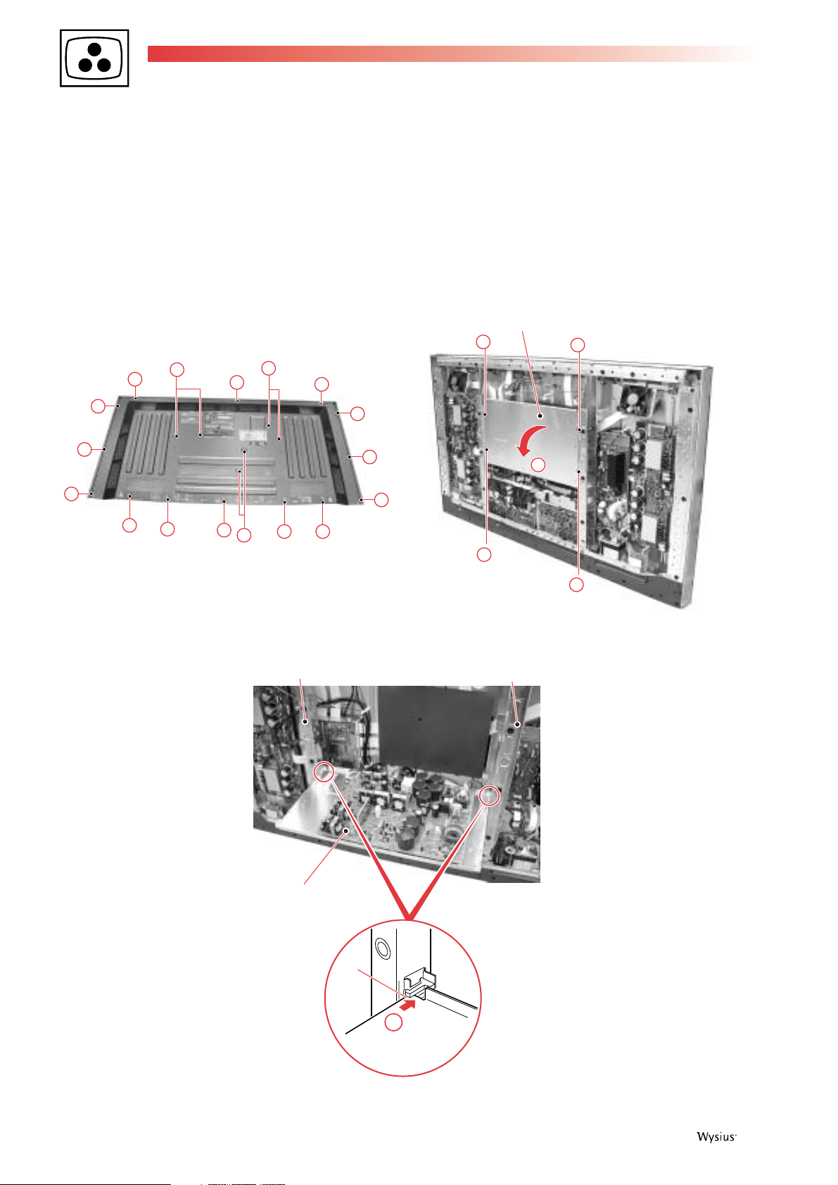
DISASSEMBLING THE MODULES
SW Power Supply Module
1 Remove the Rear Case (50M). (Screws x 20) fig. 1
2 Remove the four screws. fig. 2
3 Remove the SW Power Supply Module. fig. 2
4 Insert the SW Power Supply Module into the slits of Sub Frame L and R. fig. 3
1
1
1
1
1
1
1
1
1
1
1
1
1
1
1
1
1
SW Power Supply
Module
3
2
2
2
2
Sub Frame L
Slit
SW Power Supply
Module
Sub Frame R
4
SW Power Supply
Module
fig. 1
fig. 2
fig. 3
Page 7

First issue 09 / 03 7
DIGITAL VIDEO Assembly
1 Remove the Rear Case (50M). (Screws x 20) fig. 1
2 Remove the SW Power Supply Module. (Connectors, Screws x 4) fig. 2 and fig. 3
3 Remove the 11 screws. fig. 4
4 Remove the one screw. fig. 5
5 Remove the Terminal Panel M. fig. 5
6 Remove the SLOT TMM SERVICE Assembly. fig. 6
7 Remove the four screws. fig. 6
8 Remove the one screw to remove the switch. fig. 6
9 Remove the connectors and binders, and remove the RGB Base with PCB Assembly. fig. 6
10 Remove the DIGITAL VIDEO Assy. (Connectors, circuit board spacers x 6) fig. 7
3
3
3
3
3
3
3
Terminal panel M
4
5
RGB Assy
SLOT TMM SERVICE Assy
RGB base
7
7
8
7
7
6
9
10
DIGITAL VIDEO Assy
fig. 4
fig. 5
fig. 6
fig. 7
Page 8
8 First issue 09 /03
Y DRIVE Assembly
1 Remove the three screws. fig. 8
2 Loosen the Rivet. fig. 8
3 Remove the Lead Cover. fig. 8
4 Pull out the Flexible Cable. fig. 8
5 Detach the lower part of the Front Case 50 so that it can swing open hinged at the top. fig. 9
6 Remove the Front Case 50. fig. 9
7 Remove the Rear Case (50M). (Screws x 20) fig. 1
8 Remove the Y DRIVE Assy. (Connectors, Screws x 8) fig. 10
X DRIVE Assembly
1 Remove the Rear Case (50M). (Screws x 20) fig. 1
2 Remove the X DRIVE Assy. (Connectors, Screws x 8) fig. 11
2
3
Turn the Rivet, taking care not to push
on it, because pushing on it may set
the Rivet to its original position.
Remove the Lead Cover together
with the Rivet when the Rivet is fully
loosened.
Rivet
1
Front Case 50
Lead Cover
Lead Cover
SIDE KEY
Assy
44
5
6
Front Case 50
Aluminum
Materials
The hook of the Front Case 50 is
fixed with the Rear Case (50M) and
the aluminum material, as shown in
the illustration.
Rear Case
(50M)
8
8
8
8
Y DRIVE Assy
8
2
2
X DRIVE Assy
2
2
fig. 8
fig. 9
fig. 10
fig. 11
Page 9
First issue 09 / 03 9
BOARD LOCATION
DIGITAL VIDEO
Assy
BRIDGE B
Assy
ADR CONNECT D
Assy
CLAMP C
Assy
FRONT KEY
TMM Assy
SP OUT R
Assy
SP OUT L
Assy
CONTROL TMM
Assy
KEY
CONNECTOR
Assy
IR RCA Assy
CLAMP D
Assy
CLAMP B
Assy
TMM AUDIO
Assy
X CONNECTOR (A)
X CONNECTOR (B)
Assy
MX LED
Assy
X DRIVE
Assy
SLOT TMM SERVICE
Assy
ADR CONNECT A
Assy
Y DRIVE
Assy
SCAN (A)
Assy
SENSOR
Assy
BRIDGE A
Assy
SCAN (B)
Assy
ADR CONNECT B
Assy
ADR RESONANCE
Assy
SUB ADDRESS A
Assy
SUB ADDRESS B
Assy
ADR RESONANCE
Assy
ADR CONNECT C
Assy
ADR CONNECT D
Assy
CLAMP A
Assy
ADR CONNECT C
Assy
I/O TMM
Assy
RGB Assy
SLOT CONNECTOR
Assy
SW POWER SUPPLY
Module
BRIDGE C
Assy
BRIDGE D
Assy
ADR CONNECT B
Assy
ADR CONNECT A
Assy
Assy
Page 10
10 First issue 09 /03
DIAGNOSTIC
LED
Normal status
Error Status
This is an easy self-diagnostic function by Light Emitting Diode. When PDP does not operate, it shows a reason.
However, it is the simple version. It may not be perfect though regrettable.
Blink of GREEN Light Emitting Diode.
(Ex.: IIC communication NG of MODULE microcomputer. )
Blink of RED Light Emitting Diode
LED STATUS COMMENTS
REDThis indicator is red during standby mode
GREEN This indicator turns to green when the unit is in the FEB mode.
ORANGE This indicator turns to green when the unit is in the STAND-ALONE mode.
Normal Status
Slowly flashes GREEN Power-Management function is operating.
The number of times of blink The reason of a SHUTDOWN
1Communication NG with PANEL microcomputer
2 IIC communication NG of MODULE microcomputer
3Dew condensation NG
4 High temperature NG
5
FAN NG
FAN UNIT PD or Connection fault of the cable to FAN Assembly
6Communication NG with MODULE microcomputer
7Communication NG with WIDE microcomputer
8 IIC communication NG of MAIN microcomputer
9Connection fault of the cable to AUDIO Assembly
It is mainly various poor communications. It is possible to carry out power on again
Green lighting 200ms
The light is not switched on 3s
Blank 100ms Green lighting 200ms
The number of times of blink
The chief reason of a power down
1 Y-DRIVE NG
2
X-DC/DC CONVERTOR NG
Y-DC/DC CONVERTOR NG
3
4 X-DRIVE NG
5POWER SUPPLY NG
6
ADDRESS NG
7ADDRESS RESONANCE NG
8
DC/DC CONVERTOR (DIGITAL) NG
If you switch on a power on again, you once have to shut the main power supply.
Page 11
First issue 09 / 03 11
(Ex.: 1st -> Y-DC/DC CONVERTOR, 2nd -> Y-DRIVE)
Update status
This is in the special state about update of a firmware.
HDCP PROTECTION
Red lighting
200ms
Blank 3s
Blank 1s
Blank
100ms
Red lighting
200ms
Red lighting
200ms
1st 2nd
Slowly flashes
GREEN and RED
Quickly flashes
GREEN and RED
Updating standby or updating end of the Main microcomputer
Or updating end of the Main microcomputer
Main microcomputer is under update.
GREEN When updating data other than the Main microcomputer, it will be in this state
LED STATUS COMMENTS
Normal Status
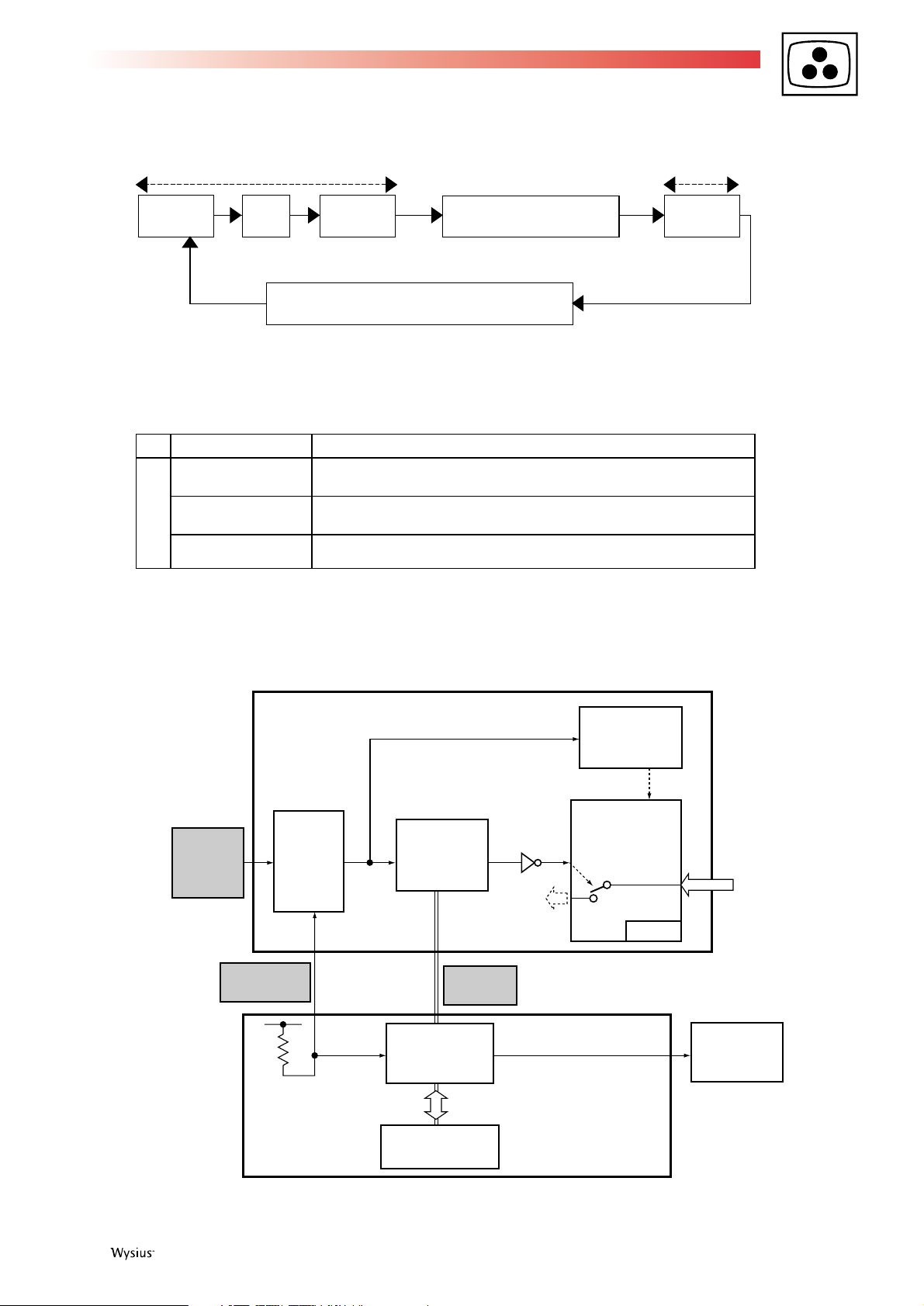
The detection block of abnormalities
POWER SUPPLY
REGULATOR
SHARP PQ3DZ13
TMDS Rx
Si907B
LOGIC
Circuit
TC74VHC02
MAIN
microcomputer
Detect A.
Rear Case
Open detect
Detect B.
SLOT ST2
Detect C.
PORT I/O SW1
OUTPUT ENABLE
POWER SUPPLY
Module
The history of a LOCK
mechanism of operation
E2PROM (Main)
PORT I/O
EXPANDER
CXA
HDCP key
POWER CONTROL
H : ACTIVE
SW3 S W1
VIDEO
SIGNAL
DVI
TMDS
3.3V
I2C
OUTPUT ENABLE
Page 12

12 First issue 09 /03
Detection in protection mode
The structure of three detections was prepared.
a. Opening of a Rear case is detected by mechanical switch.
b. Simple logic via a connector.
c. It is necessary to control IC by I2C from MAIN microcomputer.
Detection of B and C is for not operating SLOT independently.
Protection mode
When operation of abnormalities is detected, the MAIN microcomputer memorizes a history to E2PROM (MAIN). And it will change to
protection mode.
Light Emitting Diode blinks as follows at the time of protection mode.
Even if you are going to supply AC again, it goes into protection mode again by the history memorized by E2PROM.
Release in protection mode
A procedure is shown below.
1. Pushing INPUT of BODY-KEY is continued 5 seconds or more.
2. Light Emitting Diode changes to lighting of the red that shows a standby state from blink in protection mode.
3. You have to push the following keys in order within 5 seconds from red lighting.
VOL - -> INPUT -> VOL+ -> POWER ON
CAUTION:
PDP will return to protection mode again, when release is impossible within 5 seconds and a mistake is made in pushing body-key.
Red 200 ms
Blank 1100 ms
Blank 100 ms Green 200 ms
Page 13

First issue 09 / 03 13
BLOCK DIAGRAM
GENERAL BLOCK DIAGRAM
DC-DC CONVERTER
MODULE
IC1401 (IC31R)
SUB-FIELD CONV.
for RIGHT with FIELD MEM.
IC1191
FLASH
ROM
IC1207
MODULE
UCOM
V+5V_STB
V+3V_D
V+3V_D
V+3V_IC V+2V_IC
IC1301 (IC31L)
SUB-FIELD CONV.
for LEFT with FIELD MEM.
V+3V_IC V+2V_IC
V+3V_IC
X1801
V+3V_D
+12V
V+5V_STB
+12V
V+5V_D
V+3V_D
V+2V_D
V+3V_D
V+2V_D
V+5V_STB
CLK GEN
TXD0/RXD0
RE SR_UP
TXD/RXD
BA2:9
BB2:9
GA2:9
GB2:9
RA2:9
RB2:9
BIT0:3
ADLCLK UR
ADLCLK_UL
ADL LE UR
ADL_LE_UL
ADL_LE_DL
RELAY
XDRV_SIG
YDRV_SIG
SCAN_SIG
D10D11D15
D7
D18
D6
D2
D14
D4
D3
D13
D17
D8
D12
D1
D9
D16
IIC
LED_SIG
IC1703
XY DRV SEQUENCE
PATTERN GEN.
IC6501
BUFFER IC
CLK/LE
DRIVERICDRIVER
IC
DRIVERICDRIVER
IC
DRIVERICDRIVER
IC
DRIVERICDRIVER
IC
DRIVERICDRIVER
IC
IC6601
BUFFER IC
CLK/LE
DRIVERICDRIVER
IC
DRIVERICDRIVER
IC
DRIVERICDRIVER
IC
DRIVERICDRIVER
IC
DRIVERICDRIVER
IC
VADR2 VADR2
BGA1
CLAMP
VADR2
CLA1
CLAMP
AA1 AB1
VADR2
SAB1
ADR_CON
SAB3
SAB2
+60V
IC6901
BUFFER IC
CLK/LE
DRIVERICDRIVER
IC
DRIVERICDRIVER
IC
DRIVERICDRIVER
IC
DRIVERICDRIVER
IC
DRIVERICDRIVER
IC
IC6801
BUFFER IC
CLK/LE
DRIVERICDRIVER
IC
DRIVERICDRIVER
IC
DRIVERICDRIVER
IC
DRIVERICDRIVER
IC
DRIVERICDRIVER
IC
DRIVER
IC
Q6706 to Q6711
VADR_GEN
VADR2
K1
VADR2
VADR2
BGC1
CLAMP
VADR2
CLC1
CLAMP
IC6201
ADD
SEL_PULSE
IC6202
ADD
SEL_PULSE
IC6203
ADD
SEL_PULSE
IC6204
ADD
SEL_PULSE
IC6205
ADD
SEL_PULSE
IC6206
ADD
SEL_PULSE
VCC_VH
IC5V
VCC_VH
IC5V
VCC_VH
IC5V
VCC_VH
IC5V
VCC_VH
IC5V
VCC_VH
IC5V
SCAN
IC6001
ADD
SEL_PULSE
IC6002
ADD
SEL_PULSE
IC6003
ADD
SEL_PULSE
IC6004
ADD
SEL_PULSE
IC6005
ADD
SEL_PULSE
IC6006
ADD
SEL_PULSE
VCC_VH
IC5V
VCC_VH
IC5V
VCC_VH
IC5V
VCC_VH
IC5V
VCC_VH
IC5V
VCC_VH
IC5V
PSUS
SCAN
LOGIC
BLOCK
+RESET Block
IC2206
Pulse Module
OFFSET
BLOCK
Photo Coupler
BLOCK
Y-SUS
MASK
BLOCK
IC2214
Pulse Module
Y2
Y-SUS
MASK
BLOCK
Y6
Y1
Y3
Y4
Y5
DC/DC
CONV
BLOCK
+5V
VSUS
+5V VSUS+15V
VCP
VCP
+15V
V_IC5V
SOFT-D
BLOCK
+15V
V_OFSVC_VF+
PSUS
PSUS
Scan Signal
Drive
Signal
VCC_V
H
VCC_VH
V_IC5V
V_IC5V
VCC_VH
V_IC5V
V_OFS
VC_VF-
VC_VF-
VC_VF+
Drive
Signal
+5V VSUS+15V
Co2
Co1
+13.5V
+6.5V
+15V
+12V
VADR
-9V
Cs101
Cs102
Css104
Css
Q125
Switching
Q127
Switching
BA2:9
BB2:9
GA2:9
GB2:9
RA2:9
RB2:9
SD RAM
16M
SD RAM
16M
IC5301(IC30)
IC5102(IC101)
SD RAM
16M
SD RAM
16M
3State Buffer
232C
DRIVER
+3V,+5V,-5V,+9V
+3V,+2V
STB+5V
PC
AUDIO SIGNAL
REG
T1
T2
T4
T3
T5
T6
13.5V,6.5V,-9V
12V,9V, 5V,3V
Plug&Play
E2PROM
9V, 5V,
3V
12V,13.5V,-9V,
6.5V,STB5V
12V,
STB5V
12V,13.5V,
-9V,6.5V
STB5V
N1 DET
C1
R2
R3
R4
AC1
AD1
L OUT
C3
SPR1
KL2
KL1
RE1
SW1
TE1
DIGITAL ASSY
Y DRIVE ASSY
SCAN B ASSY
(LOWER)
SCAN A ASSY
(UPPER)
THERMAL SENSOR ASSY
ADDRESS CONNECT B ASSY
ADDRESS CONNECT A ASSY
ADR RESONANCE ASSY
RGB ASSY
K2
ADDRESS CONNECT D ASSY ADDRESS CONNECT C ASSY
CLAMP C ASSY
CLAMP A
ASSY
BRIDGE C ASSY
BRIDGE A ASSY
CONTROL ASSY
SP OUT R
ASSY
IR TMM
ASSY
KEY CONNECTOR ASSY
FRONT KEY
TMM ASSY
PSUS
I/O ASSY
TRAP SW
IC1101
PANEL UCOM
ADL _LE_DR
ADLCLK_DR
ADLCLK_DL
TEMP
KL_D0:2
KL_U0:2
EXTERNAL
CONTROL
IC6801
BUFFER IC
CLK/LE
DRIVERICDRIVER
IC
DRIVERICDRIVER
IC
DRIVERICDRIVER
IC
DRIVERICDRIVER
IC
DRIVERICDRIVER
IC
IC6901
BUFFER IC
CLK/LE
DRIVERICDRIVER
IC
DRIVERICDRIVER
IC
DRIVERICDRIVER
IC
DRIVERICDRIVER
IC
DRIVERICDRIVER
IC
VADR2
+60V
SAA1 SAA2
ADR_CON
SAA3
K1
VADR2
VADR2
BGB1
CLAMP
VADR2
CLB1
CLAMP
AC1
AD1
Q6706 to Q6711
VADR_GEN
IC6601
BUFFER IC
CLK/LE
DRIVER
IC
DRIVERICDRIVER
IC
DRIVERICDRIVER
IC
DRIVERICDRIVER
IC
DRIVERICDRIVER
IC
IC6501
BUFFER IC
CLK/LE
DRIVERICDRIVER
IC
DRIVERICDRIVER
IC
DRIVERICDRIVER
IC
DRIVERICDRIVER
IC
DRIVERICDRIVER
IC
VADR2
VADR2
VADR2
BGD1
CLAMP
VADR2
CLD1
CLAMP
+RESET
Pulse
Block
DC/DC
CONV
BLOCK
+5V
Drive
Signal
LOGIC
BLOCK
IC3200
Pulse
Module
X_SUS
MASK
IC3201
Pulse
Module
X_SUS
MASK
+15V
+5V
V_SUS
+15V
+5V
V_SUS
X 1
X 2
X 3
X 4
P_SUS
P_SUS
Drive
Signal
VCP
VCP
v_RN
+15V
v_RN
Co3
Co4
Co5
Co6
VSUS
STB5V
Cs103 Cs104
Cs105
Cs106
LIVE
NEUTRAL
RL101
POWER RELAY
RC101
PRIMARY
SECONDARY
Q128
Q131
M107
Switching
Cl117
Switching
VSUS_CONT
IC5601
WIDE UCOM
IC5505
MAIN UCOM
IC5001(IC102)
IC4803
PLD for SYNC
FLASH
ROM
S3
S1 S2
+11V
+15V,+5VSTB
A1
A_Mute2
R_Audio
L_Audio
+5VSTB
A3
R_OUT
L_OUT
IC8601
POWER AMP
A6
FAN_D
A7
FAN MUTE
IC8701
REGULATOR
+5V_AD/RGB
A5
AUDIO_NG
TEMP3
FAN_NG
+15V
STB+5V
STB+5V
R6
V1
E2PROM
EXPANDER
DVI
REG
+7V,-8V
+3V, +5V, -5V
I2C-BUS
R9
R1
R8
I2C-BUS
AB1
AA1
L OUT
CLAMP
CN901
K3
SPL1
L1
POWER SUPPLY MODULE
SUB ADDRESS A ASSY
ADR RESONANCE ASSY
ADDRESS CONNECT C ASSY
ADDRESS CONNECT D ASSY
TMM AUDIO ASSY
VIDEO SLOT TMM ASSY
SLOT CONNECTOR
ASSY
V MID CLAMP Block
X DRIVE ASSY
X CONNECTOR
A ASSY
X CONNECTOR
B ASSY
SUB ADDRESS B
ASSY
SP OUT L
ASSY
MX LED ASSY
K3
ADDRESS CONNECT B ASSY
ADDRESS CONNECT A ASSY
CLAMP D ASSY
CLAMP B ASSY
BRIDGE D ASSY
BRIDGE B
ASSY
STB+5V
12V,5V
CLAMP
AUDIO
Plug&Play
E2PROM
2-1 SEL
IC8602
REGULATOR
+11V+15V
FAN
LPF IC
V2
PANEL LINK
RECIEVER
GAIN AMP
IC4402
MATRIX
IC4603
A/D PLL AMP
6M LPF
SW POWER SUPPLY
Block
+5V_AD/RGB
K2
Page 14

14 First issue 09 / 03
RGB BLOCK DIAGRAM
13.5V
V+12V V+12V
IC4004
6.5V
-9V
IC4110
(24LCS21A)
Plug&Play
ROM
(TC74VHC541)
TTL
Conv.
INPUT1
Input DET.
IN1DET
WP_SW
Time
Circuit
IC4108
(BA7657F)
RGB
2-1 SW
STB+5V
INPUT1
Component
/RGB
INPUT2
Component
/RGB
Terminator
SW
Audio
Input
Mute
A_MUTE1
EXT_INT
VOL
IC4103
(TC4052BF)
EXT/INT
SEL
IC4104
(TA7630P)
Pre-Amp.
IC4103
(TC4052BF)
FIX/VAL
SEL
Audio
Output
Terminator
SW
INPUT1
Monitor
Out
V-5V V-5V
IC4001
FIX_VAR
A_MUTE2
AUDIO_NG
STB+5V
V+9V V+9V
IC4002
V+5V V+5V
IC4003
V+3.3V V+3.3V AD
IC4005
V+3.3V V+3.3V PLD
IC4006
Audio Amp.
Analog RGB HV / YPbPr
Digital RGB
6M LPF
GeonSYNC(1)
GeonSYNC(2)
2-1
SEL
SYNC SEP
Circuit
EXT_INT
CBLK_MAT
CBLK_LPF
CLP_MAT
CLP_AMP
CLP_AMP
HOLD
IC4402
(CXA2101AQ)
MATRIX ~35M
(3-1 Select)
IC4603
(CXA3516R)
A/D PLL AMP
(2-1 Select)
IC5001
(???????)
IC102
IC5102
(PE5066ACK)
IC101
(LCX125)
CLK SEL
SD RAM
16M
SD RAM
16M
SCP-IN
(31)
HOLD(106)
G/YOUT(2)
B/CbOUT(1)
R_CrOUT(3)
SYNCIN(111/112)
CLPIN(113)
XUNLOCK
(104)
1/2CLK
(101)
DIVOUT
(103)
SDA(56)
SCL(55)
ACL AMP
ACL
I/O ASSY
(LCX541)
2-1
Selector
Buffer
Clamp
SW
DIVOUT(32)
HD_SEP(106)
VD_SEP(107)
CLP_SEP(99)
HPOL(98)
VPOL(97)
HSTATE(96)
VSTATE(93)
CLP_SW1(91)
CLP_SW2(92)
HD_30(72)
HD_PLL(27)
VD_AD(8)
HD_RGB(41)
VD_RGB(42)
HD_PLK2(117)
HD_PLD(119)
VD_PLD(118)
CLP1(5)
CLP_AMP(28)
CLP_MAT(111)
CBLK_MAT(110)
CBLK_LPF(109)
HDLD_PLL(31)
CLP2(6)
HBLKT(7)
VBLKT(8)
VD_PLK2(116)
-HS(100)
+HS(101)
+VS(102)
IPKILL(68)
CS(67)
FILM(70)
HWR(66)
RD(65)
RES(62)
UD[8:15]
UA[0:20]
YI[0:7]
CLP1(278)
CLP2(279)
HBLK1(280)
VBLK1(282)
VD_AD(53)
HD_AD(52)
PBI[0:7]
PR[0:7]
YI[0:7]
PBI[0:7]
PR[0:7]
YP[0:15]
PBP[0:15]
PRP[0:15]
RA_IP[0:7]
GA_IP[0:7]
BA_IP[0:7]
FDET(60)
VACT(61)
WAIT(62)
EMG_IP(67)
CS(66)
HWR(64)
RD(65)
RES(56)
YP[0:15]
PBP[0:15]
PRP[0:15]
HI(57)
VI(58)
FI(64)
HI(168)
VI(167)
FI(166)
HP(55)
VP(56)
HP(170)
VP(169)
CLK(3)
RAO[0:7]RBO[0:7]
GAO[0:7]GBO[0:7]
BAO[0:7]BBO[0:7]
VCLK(132)
DEO(99)
HDO(98)
VDO(97)
CLK(236)
IC4803
(EPM3256ATC144-10)
PLD for SYNC
V+3VD
DC/DC
Converter
IC31
(1/2)
IC31
(2/2)
V+2VD
SD RAM
16M
SD RAM
16M
IC5301
(PD6357B)
IC30
IC5602
(MEM29L800TA-90PFIN)
Flash ROM
100MHz
X'tal
VD Shift
HWR_DLAY
IC5502
(24LC64(I)SN
EEP ROM
THERMO
SENSOR
FAN KEY LED RS-232C REM
Main UCOM
Write Connector
Wide UCOM Write Connector
(PS9248N)
RST IC
IC5504, IC5509
(74HCT00)
SYNC SEL
TC7W126FU
TC7W126FU
Module UCOM
(LM50C1M3)
Thermo
Sensor 2
(M5223)
OP AMP
IC5501
(TC74WHTC541AFT)
3.3V 5V Converter
IC5503
(TC74WHTC541AFT)
5V 3.3V Converter
RST IC
AND
DIGITAL VIDEO
ASSY
RGB ASSY
IC5601
(HD64F2328VF)
Wide UCOM
IC5505
(M3062FGAFP)
Main UCOM
DPMS(7)
H_SYNC(5)
H_SYNC(6)
AUDIO_NC(42)
(E)SDA(82)
(E)SCL(81)
EEPRST(83)
TEMP(94)
FAN_NG(48)
FAN(3)
KEY1_SCAN(20)
LED_G(37)
LED_R(38)
CNVSS(9)
BUS(34)
RXD1(32)
TXD1(31)
RST(12)
CB_MUTE
(50)
REM(18)
REQ_MD(19)
POWER(53)
PNL_MUTE(60)
WE_MD(72)
RXD0(36)
TXD0(35)
TEMP2(95)
BUSY30(55)
RESET(61)
WAIT_FLASH(102)
A13_FLASH(70)
CS_FLASH(69)
RY/BY(102)
WACT_FRCT(32)
HD_W(117)
VD_W(34,73)
DE_W(33,72)
H(119)
VI(31)
FI(118)
CS_30(66)
IC_RST(126)
RDB(91)
HWRS(92)
SGLB_AD(79)
HWR_30
(88)
D_CLK(63)
D_RXD(61)
WU_CE(29)
FEW_CE(60)
MD2(125)
EXT_RXD(62)
EXT_TXD(60)
REQ_WU(71)
D_BUSY(64)
DLK_PLL(105)
PLL_OE(33)
TXD_WU(97)
SCK_WU(101)
RST2(75)
IN5DET(49)
BUSY(54)
REQ_WU(74)
WE_WU(71)
RST_WU(70)
MD2(69)
FWE(68)
WU_CE(47)
OSD_CE
(45)
DIN_SEL
(66)
ACL_SW(58)
SDA(30)
SCL(29)
SIGRST(88)
FR_SEL(51)
PLD_CE(90)
TXD(1)
CLK(2)
H_POL(79)
V_POL(80)
SYNC_ST(85)
RGB_SEL(52)
IN1DET(40)
WP_SW(21)
VOL(4)
EXT_INT(76)
FIX_VAR(84)
A_MUTE1(77)
A_MUTE2(78)
IN3DET(36)
IN4DET(37)
SDIN_SEL(67)
SLOT_ST(93)
SLOT_ST2(22)
UA [0 : 20]
UD [0 : 15]
ULK_PLL(30)
HD_U(140)
VD_U(139)
CLK(125)
FR_SEL(134)
PLD_CE(137)
SCK(128)
TXD(138)
H_POL_U(132)
V_POL_U(131)
SYNC_ST(136)
MCLKI(242)
HIS(300)
CLKI(286)
DEI(296)
HDI(297)
VDI(299)
OSD_RXD(21)
OSD_CLK(22)
OSD_CE(23)
HWRB(301)
RDB(302)
RESETB(303)
CS4B(1)
OSD_V(49)
MCLKO(152)
CLK2A(247)
RA[0:9]RB[0:9]
GA[0:9]GB[0:9]
BA[0:9]BB[0:9]
OSDH(62)
CLKOUT(88)
DEO(92)
HDO(91)
VDO(90)
RAI[0:7]RBI[0:7]
GAI[0:7]GBI[0:7]
BAI[0:7]BBI[0:7]
(LT1399CS)
3CH
Video
Amp.
2-1
SEL
2-1
SEL
(LCX541)
Line Buffer
6M
LPF
SECAM
FLT
Audio
Input A
Audio
Input B
DVI
Y/C
VIDEOINVIDEO
OUT
(TFP201H)
TMDS RECEIVER
Slot
State
6M LPF
3L Y/C
Chroma Decode (4-1 Select)
EEPROM
3D Y/C&CNR
6M LPF
SD RAM
Expan.
DBR
3D_RST
I2C BUS
DVI_PS
VY_SBL
IN4DET IN3DET
Page 15

First issue 09 / 03 15
DIGITAL VIDEO BLOCK DIAGRAM
IC5301
(PD6357)
IC30
Line
Buffer
IC1191
Flash ROM
IC1301 (IC31 L)
(PD6358)
DRAM
IC1401 (IC31 R)
(PD6358)
DRAM
IC1703 (IC23)
(PE5064)
IC1101
(HD64F2328VF)
Panel Microcomputer
CN1201
3.3V 5.0V5.0V 3.3VReset IC
Reset IC
THERMAL
SENSOR
Assy
SW POWER SUPPLY Module
OR
EEP
ROM
DC/DC
Converter
Block
5V
OR
AND
AND
IC1207
(M30624FGAFP)
Module Microcomputer
IC5505
(M30624FGAGP)
Main
Microcomputer
Address Data
Address Data
ADR CONNECT A - D
Assy (Left section)
ADR CONNECT A - D
Assy (Right section)
Y DRIVE Assy
X DRIVE Assy
RESONANCE
Assy
5V
5V
PC_VIDEO
ADR_K_EMG
STOPB
3.3V
3.3V
12V
ADR K PD U
ADR PD
APD MUTE
EXD TXD
RST2
RST PU
EXD RXD
RESET
RESET
RXD
BUSY
REQ_PU
ADR K PD D
DEW DET
RELAY
TEMP1
STB5V
STB5V
STB5V
3.3V
2.5V
3.3V
3.3V
3.3V
VD
HD
VD 31
APLR
STB5V
2.5V
IIC BUS
RGB 2 phase 10 bit
VD
HD
DE
CLK
Address BUS
Data BUS
Control Signal
RXDO
REM
PM_ST
PN_MUTE
MAX_PLS1
DITHER
MOD_SW
POWER
MAX_PLS2
TXDO
REQ_MD TXDO
WE_PN
RXDO
EXT_RXD
EXT_TXD
Reflesh-rate
Det.
AC_OFF
PD_TRIGGER
DCC_PD
Panel W/B ADJ.
Hour/Pulse meter
pn
Address
Resonance
Control
Sustain
Control
RGB ASSY DIGITAL VIDEO ASSY
DIG. ADR. PD
Page 16

16 First issue 09 /03
X DRIVE BLOCK DIAGRAM
23
21
5
7
9
11
13
15
17
19
PN_MUTE
XNR-U
XSUS-B
XSUS-U
XSUS-D
XSUS-G
XSUS-MSK
XCP-MSK
XNR-D1
XNR-D2
CN3001
X2
1
2
3
4
8
11
CN3101
X1
XNR_U
XNR_U
2
4
5
3
6
6
5
2
3
4
9
IC3004
TC74ACT540FT
IC3008
TC74ACT541FT
18
17
14
14
15
18
17
16
16
15
1
5
2
3
4
6
8
9
7
10
IC3008
PE1012A
20
23
22
21
19
17
16
18
15
2
3
4
5
7
8
6
9
IC3001
TC74ACT541FT
IC3102
HCPL-M611
IC3101
TC74ACT541FT
IC3200
STK795-470
Pulse Module
IC3201
STK795-470
Pulse Module
T3701
VRN D-D CONV.
XCP-MSK
XSUS-MSK
VCP
PLD
SUSOUT A
37-40
29,30
K3105
PSUS
K3107
IC3103,IC3104
TND301S
Q3103,
Q3107
Q3104,
Q3109
Q3105,
Q3124
Q3106,
Q3125
SUSOUT B
37-40
29,30
K3106
IC3106,IC3107
TND301S
Q3110,
Q3114
Q3111,
Q3115
Q3112,
Q3126
Q3113,
Q3127
To
X CONNECTOR
ASSY
IC3110
TND301S
IC3113
TND301S
charge pump
circuit
From DIGITAL VIDEO ASSY
Photo
coupler
2-9 11-18
+15V
DGND
XDRIVE_PD
XDC_DC_PD
VSUS
SUSGND
SUSGND
SUSGND
P.D.
DET.
18
17
16
15
13
12
14
11
14
16
18
20
14
16
18
20
VSUS 225V
VRN UVP
VRN OVP
Q3116
Q3120
Q3122
Q3128
XNR-D1
XNR-D2
VRN-300V
X DRIVE
Page 17

First issue 08 / 03 17
Y DRIVE BLOCK DIAGRAM
CLR
CLK
OC1
OC2-1
LE
AB
SI1
SI2
Photo Coupler
Photo Coupler
Photo Coupler
Photo Coupler
Photo Coupler
Photo Coupler
Photo Coupler
Photo Coupler
VH D-D CONV.
Pulse Module
(STK795-470)
IC2206
YSUS-MSK
OC2-2
PN_MUTE
YPR-U1
YPR-U2
YSUS-B
YSUS-U
YSUS-D
YOFS
YSUS-G
YCP-MSK
YSUS-MSK
YSOFT-D
DEW_DET
Y2
IC2005
TC74ACT541FT
IC2007
TC74ACT540FT
IC2004
YPR-U1
TC74ACT541FT
Pulse Module
(STK795-470)
IC2214
14
16
18
20
14
16
18
20
IC2202
HCPL-M611
IC2006
PE1013
IC2005
TC74ACT541FT
Dew DET.
circuit
Photo Coupler
OC2-2
Y3
Y5
Photo Coupler
SUS muteDET.
circuit
charge pump
circuit
Photo Coupler
VOFS D-D
CONV.
D. GND
+13.5V
SUSGND
D. GND
IC5V, VF
D-D CONV.
IC5V UVP
VOFS UVP
VOFS OVP
VH UVP
VH OVP
VOFS
VF-
IC5V
VF+
VH
YSOFT-D
YOFS
YCP-MSK
VH
VH
IC5V
+13.5V
-9V
IC2208
HCPL-M611
IC2001
TC74ACT541FT
Q2102
IC2504
TC74ACT540FT
IC2506
TC74ACT540FT
IC2503
TC74ACT540FT
IC2516
HCPL-M611
IC2501,IC2502,
IC2505,IC2510,
IC2512,IC2513,
IC2514,IC2525,
HCPL-M611
P.D.
DET.
Vsus
27
25
30
31
40
42
43
45
33
24
19
21
9
10
12
18
13
16
15
22
46
2
+15V
1
3
4
5
6
7
10
11
13
14
CN2501CN2502
To SCAN ASSY
(Lower)
To SCAN ASSY
(Upper)
-9V
YDRIVE_PD
YDC_DC_PD
VOFS_ADJ
VSUS
VSUS
SUSGND
SUSGND
YPR-U2
PSUS
SUSOUT A
VCP
TO
Y CONNECTOR
ASS'Y
SUSOUT B
37-40
37-40
29,30
29,30
IC2201
TC74ACT541FT
K2212
K2203
K2220
PSUS
IC2212
TND301S
Q2219
Q2218
IC2213
TND301S
2-9
11-18
Q2215
Q2216
Q2217
Q2226
IC2217
TND301S
Q2227
Q2220
Q2221
Q2228
Q2232
Q2233
IC2216
TND301S
YPR-U1
YPR-U2
VSUS
SUSGND
Q2210
Q2211
Q2212
Q2204
Q2205
IC2203
TND301S
IC2204
TND301S
IC2210
TND301S
Vsus
15V
5V
Vsus
15V
5V
X DRIVE
Page 18

First issue 08 / 03 18
AUDIO BLOCK DIAGRAM
TMM AUDIO ASS'Y
FAN DRIVE BLOCK
RCA AUDIO BLOCK
+15V
A1
R_AUDIO
GND
A_MUTE2
STBY
GND
L_AUDIO
+5VSTB
+5VSTB
A3
L+
GND
GND
R+
TEMP3
IC8601
POWER AMP
A6
FAN_P
FAN_D
A7
FAN_P
FAN_D
+15V
Vin Vout
Vc Vadj
FAN_Mute
( < 3.4V )
IC8701
REGULATOR
+5V_AD/RGB
A5
AUDIO_NG
TEMP3
FAN_N
FAN
+5V_AD/RGB
+5V_AD/RGB
NOR
(5.5V - 12.35V)
(3.06V - 1.66V)
IC8602
REGULATOR
+15V
Vin
+5V_AD/RGB
11V
R-
L-
+5VSTB
OP-AMP(Buf)
Page 19

19 First issue 08 /03
SUB ADDRESS DIAGRAM
+60V
ADRGND
CN8801
R8801 - R8805 Q8801
V MID SW
ADRK EMG1
Q8803, Q8831 Q8805, Q8806
+12V
DGND
ADR-B ADR EMG 1 Block
ADR-U
12V
ADR-D
ADRK. PD
CN8802
IC8801 IC8801 D8804
(DC+AC) (-AC) 5V
SW
ADR-D
(DC) CLK
ADR-U
ADR-B
+12V
IC8802 IC8802 IC8803
DGND
VADR
ADRGND
CLR
ADROUT
CN8803
IC8804
Current - Voltage
Convert Block
Over Current DET. Block
ADR Output
Resistance Load Block
P.D. Output Block
BUFF Block
Inversion
Block
Additional
Block
Conparator
(EMG : ON)
Flip / Flop
+5V REG
H : EMG1 OFF
L : EMG1 ON
H : V MID CLAMP OFF
L : V MID CLAMP ON
Conparator
(EMG : OFF)
SUB ADDRESS ASSEMBLY
Page 20

First issue 09 / 03 20
ADR RESONNANCE BLOCK DIAGRAM
+60V
+60V
+60V
+60V
CN6702
IC6704 C6703 - C6708
12V
Address Resonance Output Block
ADROUT
ADRGND
ADR B
VADR
C6720 Q6706
DGND
Q6707
+12V
IC6701 Q6701, Q6704 ADR U
ADR-B
C6721 Q6708
ADR-U
Q6709
ADR-D
SW
CN6701
ADR OUT
L6704
IC6702 Q6702, Q6705
VADR
V MID
ADR D
ADRGND
C6722 Q6710
DGND
Q6711
SW
CN6703
DGND
IC6703 Q6703, Q6712 V MID
C6716
C6718
ADRGND
ICP-S1, 0
ADR-B
Pre-Drive
ADR-U
Pre-Drive
ADR-U
Drive
ADR-D
Pre-Drive
ADR-D
Drive
ADR-B
Drive
SAFETY PART :
For continued protection against risk of fire,
replace by original part only
ADR RESONNANCE
ADDRESS CONNECTORS BLOCK DIAGRAM
ADR OUT
ADR PD
Q6502, Q6503
IC6501
CN6501
Buffer
BRIDGE ASSY
OPEN PD
HZ
LBLK
HBLK
LE
CLK
Address Module
(TCP)
Address Module
(TCP)
Address Module
(TCP)
Address Module
(TCP)
Address Module
(TCP)
DATA_R
DATA_G
DATA_B
DATA_R
DATA_G
DATA_B
DATA_R
DATA_G
DATA_B
DATA_R
DATA_G
DATA_B
DATA_R
DATA_G
DATA_B
DATA_R
DATA_G
DATA_B
DATA_R
DATA_G
DATA_B
DATA_R
DATA_G
DATA_B
DATA_R
DATA_G
DATA_B
DATA_R
DATA_G
DATA_B
HZ
LBLK
HBLK
LE
CLK
ADDRESS CONNECT.
Page 21

First issue 08 / 03 21
SIGNAL PATH
VIDEO AND SYNCHRONISATION
INPUT Input Signal Signal Route
VIDEO Signal
(480i)
VIDEO Signal
(except 480i)
PC Signal
3/4
VIDEO Signal
(NTSC)
5
VIDEO Signal
(DVI)
INPUT1
INPUT2
INPUT3
INPUT4
INPUT5
Analog Video Signal
Digital Video Signal
1/2
IC4108
BA7657F
IC4403
6M LPF
IC4402
CXA2101AQ
IC4603
CXA3516R
IC5001
PE5067A-K
IC5301
PD6357B
IC4108
BA7657F
IC4402
CXA2101AQ
IC4603
CXA3516R
IC5001
PE5067A-K
IC5301
PD6357B
IC4108
BA7657F
IC4603
CXA3516R
IC5001
PE5067A-K
IC5301
PD6357B
IC7102
UPD64082GF
IC7202
TB1274AF
IC7301
BA7657F
IC4603
CXA3516R
IC5001
PE5067A-K
IC5301
PD6357B
IC7305
SM5301AS
IC7302
M61303FP
IC7301
BA7657F
IC4603
CXA3516R
IC5001
PE5067A-K
IC5301
PD6357B
IC7507
SiI907BCQ52
IC7001
NJM2234
IC7001
NJM2234
IC7507
SiI907BCQ52
IC4108
BA7657F
IC7305
SM5301AS
IC7302
M61303FP
IC7301
BA7657F
IC7102
UPD64082GF
IC7202
TB1274AF
IC4403
6M LPF
IC4402
CXA2101AQ
IC4603
CXA3516R
IC5001
PE5067A-K
IC5301
PD6357B
Total Figure
Page 22

22 First issue 08 /03
VIDEO SLOT
ANALOG OUTPUT
(YCBR/RGB)
IN5DET
AUDIO
OUTPUT
I2C BUS
R-Y
WP SW B-Y
DVI SEL
V/Y SEL
3D RST
Reg cont
INPUT 5
DVI TERMINAL
For
Adjustment
EEPROM
3-1SELECT
2-1
SELECT
Chroma Decode
For EDID
EEPROM
LOGIC
CONV
LPF IC
SM5301AS
CN
SHELD
DET
REG
EXPANDER
CBR ADJ
3cH Gain AMP
M61303
SYNC
CONV
2-1SELECT
BA7657
3D Y/C
(SA:B8/B9)
VOLT CONV
DVI-HDCP
Receiver
SII907
Independent Detection
DE
DAC_P
CL AMP
PROT
LPFSEL (DAC)
Rear Case opening detection
Rear Case opening detection
Page 23

23 First issue 09 /03
ADJUSTMENTS
Adjusting Mode
SERVICE MODE
In this mode, picture-quality adjustments more accurate than those made on the normal user menu and various functions for
alleviating phosphor burn can be performed.
In order to use this mode, you should make PDP the stand-alone. (Or it recommends removing a communication cable with FEB.)
And PDP is made standby (OFF). (Light Emitting Diode must be red lighting.)
The following operations are made into turn in order to go into this menu:
1. It pushes “VOLUME UP” of BODY key first.
2. Next, it pushes “VOLUME DOWN” of Body key.
3. Finally it pushes “POWER ON” of BODY key.
It is necessary to perform these operations quickly. All operations need to carry out within 3 seconds.
If it puts into service mode, a display will come out to the upper left, “SERVICE MODE”(SERVICE MENU).
Operation of a service menu can be performed by the remote control that outputs the Thomson code. And the body key can operate
it also.
To select category (Picture, Screen and etc.), press LEFT or RIGHT key.
Moving a cursor with UP or DOWN key will highlight items (CONTRAST, BRIGHTNESS and etc.). To chose an item, press OK key.
When operating it by the body key, it is the same as menu operation in PC mode at the time of FEB connection.
To escape from a service menu display, press EXIT or MENU key.
Notes:
A service menu does not escape from the mode, even if a signal is lost. (Action differs from the menu for users.) In this case, only
OPTION can be operated.
Again, when a signal is inputted, it is the PICTURE MENU.
Power-Standby mode
Normal Operation mode
: Indicates each mode.
SERVICE MODE
FACTORY MODE
: Indicates a key operation on the remote control unit or the operation panel of the unit.
: Indicates an operation performed with an RS-232C command.
POWER
POWER
Within 3 seconds
MENU
MENU
<FAN>
<FAY> <AJY>
MENU
<AJN>
ADJUSTMENT MODE
Page 24

First issue 09 / 03 24
PICTURE
Picture Item
A sub menu is displayed when the following item is chosen.
In a sub menu, change of an item is possible by UP or DOWN key.
These adjustments are required for each input (INPUT1 to INPUT5) and signals.
Picture Default
Selecting “DEFAULT” by LEFT, RIGHT or OK key press display following menu
If a highlight is moved to "YES", the quality of image is reset in shipping condition. It is memorized by "O.K."
Adjustment range INPUT Item
MIN
MAX
The center value
of shipment *1
CONTRAST 0 255 128
BRIGHT. 0 255 128
H.ENHANCE 0 15 0
PC
V.ENHANCE
0
15
0
CONTRAST 0 255 128
BRIGHT. 0 255 128
COLOR 0 255 128
TINT 0 255 128
H.SHARP 0 15 8
DVI
V.SHARP 0 15
8
*1 It is a value peculiar to a product which has variation by adjustment.
Page 25

25 First issue 09 /03
WHITE BALANCE (WHITE BAL.)
White Balance Item
A sub menu is displayed when the following item is chosen.
*1 It is a value peculiar to a product that has variation by adjustment.
Picture Default
Selecting “DEFAULT” by LEFT, RIGHT or OK key press display following menu
If a highlight is moved to "YES", the quality of image is reset in shipping condition. It is memorized by "O.K."
SCREEN
Screen Item
Adjustment rangeItem
MIN
MAX
The center value
of shipment *1
R HIGH 0 255 255
G HIGH 0 255 255
B HIGH 0 255 255
R LOW 0 255 128
G LOW 0 255 128
B LOW 0 255 128
Page 26

First issue 09 / 03 26
Screen Default
Selecting “DEFAULT” by LEFT, RIGHT or OK key press display following menu
If a highlight is moved to "YES", the quality of image is reset in shipping condition. It is memorized by "O.K."
OPTION
It is moved highlight by UP or DOWN key press. O.K. can change each item after selection by UP and DOWN.
Baud Rate
This item is a baud rate setup of RS-232C. RS-232C is used for factory adjustment. Furthermore, it is used also for upgrade. It is
reference. A baud rate is changed whenever it pushes O.K.
->4800BPS->9600BPS->19200BPS->38400BPS->1200BPS->2400BPS->4800BPS->
Notes: Default is 4800BPS. Don't change this setup.
Full Mask
It is the mode in which a signal is generated inside PDP. It is white, red, green and blue. It changes by O.K. It may be useful to relief
of printing of a screen.
-> OFF -> WHITE -> RED -> GREEN -> BLUE-> OFF ->
Notes: This mode is maintained even if it escapes from service mode. Default is OFF
Adjustment rangeSignal Item
MIN
MAX
Default value
H.POSITION 0 255 128
V.POSITION 0 255 128
CLOCK 0 255 128
PHASE 0 63 32
PC
V.SIZE 0 127 0
DVI V.SIZE 0 127 0
Page 27

27 First issue 09 /03
Side Mask
It is brightness adjustment of a non-drawing part. It is at the time of the screen size “DOT BY DOT” and “4:3”. It can be adjusted
independently, R, G, B.
The default of a side mask differs from others.
When DEFAULT is a highlight, shortly after pushing O.K., it returns to a shipment value. And a value is changed and it returns to a
service menu.
Mask Control
If this mode is turned ON, a non-drawing portion will move. It is at the time of the screen size “DOT BY DOT” and “4:3”. Moreover,
whenever it turns on a power supply, a position moves. It is a kind in printing mitigation mode. It is usually ON.
Orbiter Mode
It is the mode that moves a little display position of a screen with progress of time. It carries out movement of 1 dot at intervals of
about 8 minutes. It is in a horizontal and vertical direction. Since there is fear of a nonsense claim, it is usually OFF.
Inverse Mode
It is the mode that reverses an image. In other words, it is negative & positive reversal. An effect may be in the emergency measure
of printing. Default is OFF.
Fan Control
It is the mode that changes control of FAN.
Adjustment rangeItem
MIN
MAX
Default value
R(ed).LEVEL 0 255 80
G(reen).LEVEL 0 255 80
B(lue).LEVEL 0 255 80
MODE An outline of operation
AUTO
The mode which controls FAN depending on the temperature sensor
inside PDP
MAX
It is not dependent on the sensor inside PDP.
This mode operates FAN at the maximum.
Usually, this mode is not used.
A default is AUTO.
Page 28

First issue 09 / 03 28
Hour Meter
The time when the total operated is counted.
This item counts the drive time of a panel.
The unit of drive time is 1 hour.
It can display for a maximum of 99999 hours.
At the time of factory shipments, it is 0H.
Version
The version of a firmware is displayed.
It is the following for details:
AAA: The version of a MAIN microcomputer
->The microcomputer that mainly controls a user interface
BBB: The version of a WIDE microcomputer
->The microcomputer that mainly controls scale conversion and I/P conversion of an image
CCC: The version of a WIDE flash memory
->The font data for OSD is mainly stored.
DDD: The version of a MODULE microcomputer
->The control microcomputer of a PDP module.
EEE: The version of a PANEL microcomputer
->The microcomputer for control of a panel.
FFF: The version of a PANEL flash memory
->Control sequence data of the PDP panel
Each item is expressed with a number and an easy sign. The part of this model with peculiar MAIN microcomputer and WIDE FLASH
memory.
FACTORY MODE
In this mode, adjustments necessary after changing assemblies can be made.
This mode is operated with RS-232C commands sent from the connected PC. To enter this mode, transmit the "FAY" RS-232C
command in Normal Operation mode.
To return to Normal Operation mode, transmit the "FAN" RS-232C command or press the MENU key on the remote control unit.
RS232C
Specification
Connector D-sub 9 pins
1
6 9
5
Pin No. Signal
1
NC (not connected)
2
TxD (Transmit Data)
3
RxD (Receive Data)
4
NC (not connected)
5
GND (CTS)
6
(Not connected)
7
NC (not connected)
8
V+(RTS)
9
NC (not connected)
Page 29

29 First issue 09 /03
Baud Rate
9600 bps (standard) (Switchable to 1200, 2400, 9600, 19200, 38400 bps)
Data Format
Start: 1-bit
Data: 8-bit
Parity: ODD
Stop: 1-bit
*Therefore, PC and PDP are connected with a straight cable.
Protocol
From computer to plasma display:
(1) When transmitting commands individually
STX (02 hex)+ ID (2 Byte)+ COMMAND (3 Byte)+ ETX (03 hex)
(2) When transmitting commands in batches (up to max. 3 commands).... (NOTE)
STX (02 hex)+ ID (2 Byte)+ COMMAND (3 Byte) +COMMAND (3 Byte) +COMMAND (3 Byte)+ ETX (03 hex)
(3) When transmitting direct numeric commands
STX (02 hex) ID (2 Byte) COMMAND (3 Byte) ARGUMENT (3 Byte) ETX (03 hex)
Note:
COMMAND 3 Bytes (ASCII)
ARGUMENT 3 Bytes (ASCII)
ID 2 bytes: It is ignored in this model. However, 2 bytes of character are required.
What has required waiting time is between commands.
POF -> PON: 6 second
IN1 ~ IN5: 3 second
Etc.
List of RS-232C commands
When a command is received, there is action, such as being displayed. These commands have some which operate by input video
signal limitation.
*Mask color becomes effective at POWEROFF/ON.
- RS-232C adjustment validity:
Shows availability in RS-232C adjustment (service) mode. The AJY command is needed when using these commands.
- Normal validity:
Shows availability in normal operating mode. Valid commands can be used even if they do not follow the sending of the AJY
command.
- Factory adjustment validity:
Shows availability in Factory adjustment mode. As for this mode, it will be used only at the time of exchange of a circuit
board, and a fatal condition. The FAY command is needed when using these commands. Especially factory adjustment mode
should use it carefully. If usage is mistaken, trouble will appear in a product
- Numerical direct validity:
Shows commands that, if transmitted followed by 3-digit numbers, can directly set the adjustment value.
- Up/Down validity:
Shows whether or not a command, if transmitted followed by Upn/DWn (with n a number from 0 to 9), can or cannot increase
the adjusted value by that number alone.
X or Y: Valid blank_: Invalid
NOTE: X = Not put into last memory
Page 30

First issue 09 / 03 30
Command
Name
Full
Name
RS-232C
adjustment
validity
Factory
adjustment
validity
Normal
validity
Numerical
direct
validity
Up/Down
validity
Function
AB0 ABL MODE0 Y
AB1 ABL MODE1 Y
AB2 ABL MODE2 Y
AB3 ABL MODE3 Y
AJNADJUST (SERVICE) NO
ADJUST (SERVICE) YES
X
Terminates RS-232C adjustment (service) mode
Terminates FACTORY mode
Initiates RS-232C adjustment (service) mode
Initiates FACTORY mode
AJY X
AMN AUDIO MUTE NO X X X
Turns audio mute OFF
AMY AUDIO MUTE YES X X X Turns audio mute ON
BBY VIDEO RGB YES Y Y Sets input setting to VIDEO SIGNAL:RGB
BHI BLUE HIGH LIGHT Y Y Y Y Adjusts BLUE HIGH-LIGHT
BLW BLUE LOW LIGHT Y Y Y Y Adjusts BLUE LOW-LIGHT
BRT BRIGHTNESS Y Y Y Y Adjusts brightness
BSL B SIDE MASK LEVEL Y Y Y Y Adjusts BLUE SIDE MASK LEVEL.
CFR Adjusts clock frequency Y Y Y Y Adjusts clock frequency
CL1 CLAMP MODE1 Y Y Sets clamp position to AUTO
CL2 CLAMP MODE2
YY
Sets clamp position to LOCKED
CNT CONTRAST Y Y Y Y Adjusts contrast
COLCOLOUR Y Y Y Y Adjusts colour
CP1 VIDEO COMPONENT1 Y Y
CP2 VIDEO COMPONENT2 Y Y
Sets signal format to COMPONENT2
Sets signal format to COMPONENT1
CPH CLOCK PHASE Y Y Y Y Adjusts clock phase
DSP DISPLAY X X
Displays current input signal information
DW0 DOWN 10 Y Y Y
Reduces adjustment value by 10
DWn DOWN n Y Y Y
Reduces adjustment value by n
Reduces adjustment value to minimum
DWF DOWN FULL Y Y Y
FAN X
FAY X
FCA FAN CONTROL AUTO Y Y
Puts control of fan’s rotation on AUTO
FCM FAN CONTROL MAX Y Y
Puts control of fan’s rotation on MAX
FMB FULL MASK BLUE Y
Turns full mask blue on
FMG FULL MASK GREEN Y
Turns full mask green on
FMN FULL MASK NO Y
Releases full mask
FMR FULL MASK RED Y
Turns full mask red on
FMY FULL MASK YES Y
Turns full mask white on
FRP FRESH POSITION Y Y
Initializes position adjustment data
FST FINAL SET UP (Y)
Various setups are made into a shipment default
FXO FIX OUTPUT Y Y
Fixes sound output (<-> VRO)
GHI G HIGH Y Y Y Y
Adjusts GREEN HIGH-LIGHT
GLW G LOW Y Y Y Y
Adjusts GREEN LOW-LIGHT
GPS GET POSITION DATA X X X
Outputs position data as TxD
GSL G SIDE MASK LEVEL Y Y Y Y
Adjusts GREEN SIDE MASK LEVEL
GS1 FIRMWARE INFORMATION X X
PDP information, versions of firmware
GSO GET STATUS OPTION X X X
Outputs OPTION-related data as TxD
Outputs SET UP-related data as TxD
GSS GET STATUS SET UP X X X
GWB GET WHITE BALANCE X X X
Outputs image quality and white balance
adjustment data as TxD
HCN HIGH CONTRAST NO Y Y
Turns high-contrast setting OFF
Turns high-contrast setting ON
HCY HIGH CONTRAST YES Y Y
HMD HOUR METER DISP. X X
Displays hour meter
HPS HORIZONTAL POSITION Y Y Y Y
Adjusts horizontal position
IN1 INPUT1 Y Y Y
Selects PC
IN2 INPUT2 Y Y Y
Selects DVI
I
H
G
F
D
C
B
A
Page 31

31 First issue 09 /03
MCN
Mask Control No
YY
Releases automatic mask position control setting
MCY
Mask Control Yes
YY
Applies automatic mask position control setting
MTN
Video Mute No
XXX
Turns video mute OFF.
MTY
Video Mute Yes
XXX
Turns video mute ON.
M
M00
Mask Mode Off
Y
M01
Mask Pattern 1(lamp)
Y
M02
(Color Bar)
Y
M03
(Slanting Line)
Y
M04
(W/B Measurement)
Y
M05
(W/B Ajustment)
Y
M06
(W/B Peak Measurement)
Y
M07
(Peak Measurement)
Y
M08
(Reserved)
Y
M09
(Block1)
Y
M10
(Block2)
Y
M11
(Reserved)
Y
M12
(Reserved)
Y
M13
(Reserved)
Y
M14
(Reserved)
(Reserved)
(Reserved)
Y
M51
(Full Mask White)
Y
M52
(Full Mask Cyan274)
Y
M53
(Full Mask Magenta1023)
(Full Mask Magenta98)
(Full Mask Beige)
(Full Mask Beige43)
Y
M54 Y
M55
(Full Mask Cyan1023)
Y
M56
(Full Mask Light Purple)
(Full Mask Light Purple43)
(Full Mask Azure)
(Full Mask Azure1_43)
(Full Mask Yellow)
(Full Mask Blue916)
(Full Mask Azure2_43)
(Full Mask Red)
(Full Mask Green)
(Full Mask Blue)
Y
M57 Y
M58 Y
M59 Y
M60 Y
M61
(Full Mask Black)
Y
The contents of a pattern may change without
a preliminary announcement. It is based on a
production process
M62
(Full Mask Red779)
(Full Mask Red620)
Y
M63
(Full Mask Cyan 218)
Y
M64
(Full Mask Cyan444)
Y
M65 Y
M66
Y
M67 Y
M68 Y
M69 Y
M70 Y
M71 Y
M72 Y
M73 Y
M74 Y
NRH
Digital Nr High
YY
Sets DIGITAL NR to HIGH
NRL
Digital Nr Low
YY
Sets DIGITAL NR to LOW.
NRM
Digital Nr Middle
YY
Sets DIGITAL NR to MIDDLE.
N
NRN
Digital Nr Off
YY
Turns DIGITAL NR OFF
OFY
Offset Mode Yes
X
Initiates OFFSET (FACTORY) mode
OMN
Orbiter Mode No
YY
Turns orbiter mode OFF
Turns orbiter mode YES
OMY
Orbiter Mode Yes
YY
O
Command
Name
Full
Name
RS-232C
adjustment
validity
Normal
validity
Numerical
direct
validity
Up/Down
validity
FunctionFactory
adjustment
validity
Page 32

First issue 09 / 03 32
Command
Name
Full
Name
RS-232C
adjustment
validity
Normal
validity
Numerical
direct
validity
Up/Down
validity
FunctionFactory
adjustment
validity
PBH Panel Blue High Y Y Y
Adjusts BLUE HIGH-LIGHT
Adjusts GREEN HIGH-LIGHT
Adjusts RED HIGH-LIGHT
Adjusts RED LOW-LIGHT
Adjusts GREEN LOW-LIGHT
Adjusts BLUE LOW-LIGHT
PBL Panel Blue Low Y Y Y
PCY Pc RGB Yes Y Y
Sets input setting to 4.3 (SETTING:VGA or XGA)
Sets input setting to wide (SETTING:
WVGA or WXGA)
PGH Panel Green High Y Y Y
PGL Panel Green Low Y Y Y
PLN Bright Enhance Off Y Y
Turn center-brightness enhancement function OFF
Turn center-brightness enhancement function ON
PLY Bright Enhance On Y Y
POF Power Off Y Y Y
Turns power OFF
PON Power On Y
Turns power ON. ONLY stand-by
PRH Panel Red High Y Y Y
PRL Panel Red Low Y Y Y
PS1 Power Save Mode1 Y Y
Sets AUTO POWER OFF to ON.
PS2 Power Save Mode2 Y Y
Turns power management setting ON
PSN Power Save Off Y Y
Turns AUTO POWER OFF/power management
setting OFF
PT0 Panel Color Temp. Y
PT1 Panel Color Temp. Y
PT2 Panel Color Temp Y
PT3 Panel Color Temp Y
PUH Purecinema Hq Y Y
Sets FILM MODE to H.QUALITY (high quality)
PUN Purecinema Off Y Y
Turns FILM MODE OFF
Turns FILM MODE STANDARD
PUS
PWY
Purecinema Standard Y Y
P
Pc Wide Yes Y Y
RFY Reference Yes X
Initiates REFERENCE (FACTORY) mode
RHI R High Y Y Y Y
Adjusts RED HIGH-LIGHT
Adjusts RED LOW-LIGHT
RLW R Low Y Y Y Y
R
RSLR Side Mask Level Y Y Y Y
Adjusts RED SIDE MASK LEVEL
SHP H.sharp Y Y Y Y
Adjusts H.SHARP/H.ENHANCE
SHV V.sharp Y Y Y Y
Adjusts V.SHARP/V.ENHANCE
SM0 Screen Mode 0 Y Y Y
Sets screen size to DOT BY DOT
SM1 Screen Mode 1 Y Y Y
Sets screen size to 4:3
SM2 Screen Mode 2 Y Y Y
Sets screen size to FULL
SM3 Screen Mode 3 Y Y Y
Sets screen size to ZOOM/PARTIAL
SM5 Screen Mode 5 Y Y Y
Sets screen size to WIDE
S
STD Standard W/b Y
Initializes image quality and white balance
adjustment data
TTNT Tint Y Y Y Y
Adjusts TINT
UP0 Up 10 Y Y Y
Increases adjustment value by 10.
UPn Up n Y Y Y
Increases adjustment value by n.
U
UPF Up Full Y Y Y
Maximizes adjustment value.
VOL Volume Y Y Y Y Y
Adjusts audio volume
VPS Vertical Position Y Y Y Y
Adjusts vertical position
Adjusts vertical size
VRO Variable Output Y Y
Sets audio-out to variable output
V
VSI Vertical Size Y Y Y Y
YCM 3d Y/c Motion Y Y
Sets 3D Y/C to MOTION.
Y
YCS 3d Y/c Still Y Y
Sets 3D Y/C to still.
Page 33

33 First issue 09 /03
GET commands
What are GET commands?
- They are commands used for TXD output of adjustment data and the like from the plasma display’s built-in microcomputer
to a personal computer.
- Adjustment data, etc., is output in ASCII code.
NOTE: Command names are given inside brackets < >.
- Data output format
NOTE: STX (02hex) Data Data ···· Data ETX (03hex)
<GPS> (GET POSITION DATA) – SCREEN adjustment data will be output as follows.
<GWB> (GET W/B DATA) – PICTURE and WHITE BALANCE adjustment data will be output as follows.
Order Data Size Remarks
1 H.POSITION 3byte
2 V.POSITION 3byte
3 CLOCK 3byte (NOTE)
4 PHASE 3byte (NOTE)
5 V.SIZE 3byte
(NOTE) If the current input signal is a video signal or digital RGB signal, the
adjustment data will be output as dummy data.
Order Data Size Remarks
1
2
3
4
5
Dummy data 3byte
CONTRAST 3byte
Dummy data 3byte
BRIGHT
3byte
Dummy data 3byte (NOTE)
6
COLOR 3byte
7
Dummy data 3byte (NOTE)
8
TINT 3byte
9
Dummy data 3byte
10
R HIGH 3byte
11
Dummy data 3byte
12
G HIGH 3byte
13
Dummy data 3byte
14
B HIGH
3byte
15
Dummy data 3byte
16
R LOW
3byte
17
Dummy data 3byte
18
G LOW 3byte
19
Dummy data 3byte
20
B LOW
3byte
21
H.ENHANCE (H.SHARP) 3byte
22
V.ENHANCE (V.SHARP) 3byte
(NOTE) If the current input signal is from a personal computer, the
adjustment data will be output as dummy data.
Page 34

First issue 09 / 03 34
<GSS> (GET STATUS SET UP) Set data for SET UP will be output as follows.
Order Data Size RemarksOutput
1
2
3
4
5
1byte
2byte
2byte
2byte
2byte
(NOTE)
6
1byte
7
2byte
8
1byte
9
3byte
10
11
3byte
12
1byte
13
1byte
14
15
3byte
16
1byte
17
1byte
18
3byte
19
1byte
3byte
1byte
COLOR TEMP 1: COLOR TEMP1
2: COLOR TEMP2
3: COLOR TEMP3
4: COLOR TEMP4
5: COLOR TEMP5 (NOTE)
DIGITAL NR 0: OFF, 1: LOW
2: MIDDLE, 3: HIGH (NOTE)
HIGH CONTRAST 0: OFF, 1: ON
FILM MODE Same as RS-232C command
Same as RS-232C command
(NOTE)
(REFER TO PURECINEMA)
COLOUR SYSTEM NTS
CLAMP POSITION 1: AUTO, 2: LOCKED (NOTE)
3D Y/C MODE M: MOTION
S: STILL (NOTE)
SETTING/VIDEO SIGNAL
N/A 0
N/A 0
HDTV MODE H80 1080I
N/ADon’t care
Input functions INx
Screen size 0: DOT-BY-DOT
1: 4:3
2: FULL
3: ZOOM
5: WIDE
N/A 60
N/A 60
N/A 60
N/A 60
N/A 60
(NOTE) For set data unrelated to the current input function, input signal and settings, dummy data will be output.
Page 35

35 First issue 09 /03
<GSO> (GET STATUS OPTION) Set data for OPTION will be output as follows.
<GS1> (GET STATUS 1) Set data for FIRMWARE will be output as follows.
Order Data Size RemarksOutput
1
2
3
4
5
3byte
3byte
5byte
1byte
6
1byte
7
8
3byte
9
3byte
10
11
3byte
12
3byte
13
1byte
14
15
1byte
16
1byte
17
1byte
1byte
1byte
12byte
1byte
Same as RS-232C command
N/A
N/A
N/A
N/A
N/A
N/A
N/A
PWN
1
FULL MASK
R SIDE MASK LEVEL Adjustment value
Adjustment value
Adjustment value
G SIDE MASK LEVEL
B SIDE MASK LEVEL
MASK CONTROL 1byte 0: Fixed, 1: Shifts
ORBITER MODE 1byte 0: OFF, 1: ON
INVERSE MODE 0: OFF, 1: ON
1
N
FAN CONTROL A: AUTO
M: MAX
NO CARE
DUMMY
TEMPERATURE
HOUR METER
0
Order Data Size Output
1
2
3
4
5
3byte
4byte
3byte
3byte
3byte
6 5byte
7 7byte
8 4byte
9 3byte
10 3byte
11 3byte
PDP INFORMATION MX5 (ASCII)
MODULE MICROCOMPUTER ID NO
MAIN MICROCOMPUTER ID NO
MODULE MICROCOMPUTER VERSION
MAIN MICROCOMPUTER VERSION
5691 or F691
3 figures (ASCII)
3 figures (ASCII)
3 figures (ASCII)
3 figures (ASCII)
3 figures (ASCII)
3 figures (ASCII)PANEL MICROCOMPUTER VERSION
PANEL FLASH VERSION
HOURMETER
N/A
RCA5 (ASCII)
WIDE MICROCOMPUTER
WIDE FLASH VERSION
Page 36

First issue 09 / 03 36
ADJUSTMENT REQUIRED WHEN THE SET IS REPLACED
RGB Assembly
Colour balance adjustment
DIGITAL VIDEO Assembly
1. Adjustment is unnecessary when only the DIGITAL VIDEO Assembly is replaced.
2. When the RGB Assembly is replaced at the same time as this assembly, remove the IC1204 (24LC04(1) SN-TBB) from
the old PC board of the DIGITAL VIDEO Assembly and attach it to the new PC board.
SERVICE PANEL Assembly
1. VSUS Adjustment
All of service panels have a panel identification label (VSUS data, VOFS data). Please just input this V-SUS data on the
label to "V-SUS" on service factory mode.
2. VOFS Adjustment
Please just input the V-OFS data on the label to "V-OFFSET" on service factory mode.
3. Panel white balance adjustment
Y DRIVE Assembly
Panel white balance adjustment
X DRIVE Assembly
Panel white balance adjustment
Other Assembly
(VIDEO SLOT Assembly, SW POWER SUPPLY Module, etc.)
No adjustment required.
DIGITAL VIDEO
Assembly
X DRIVE
Assembly
SLOT TMM SEVICE Assembly
Y DRIVE
Assembly
RGB Assembly
SW POWER SUPPLY
Module
Page 37

37 First issue 09 /03
ADJUSTMENTS
V-SUS adjustment
1. Turn on the unit.
2. Enter Factory mode.
FAY
3. Set the V-SUS value to that indicated on the Panel Identification label.
RFY
VSU (Value indicated on the Panel Identification label)
4. Check the V-SUS adjustment value.
GAJ: To read the V-SUS value from the output data
5. Finish making adjustments.
FST
FAN
6. Turn off the unit.
V-OFS adjustment
1. Turn on the unit.
2. Enter Factory mode.
FAY
3. Set the V-OFFSET (V-OFS) value to that indicated on the Panel Identification label.
RFY
VOF (Value indicated on the Panel Identification label)
4. Check the V-OFS adjustment value.
GAJ: To read the V-OFS value from the output data
5. Finish making adjustments.
FST
FAN
6. Turn off the unit.
Panel-White-Balance Adjustment
Input signal
Use the MASK 04 signal of the PDP.
Adjustment parameters
PANEL R HIGH/PANEL G HIGH/PANEL B HIGH
PANEL R LOW/PANEL G LOW/PANEL B LOW
Adjustment method
1. Turn on the unit.
2. Adjust the following parameters:
FAY
DIN
M04 the Mask window for adjustment is displayed.
F60
PT1
AB2
GPW Check the parameters before adjustment.
PRHxxx
PGHxxx
PBHxxx
PRLxxx
PBLxxx
PGLxxx
GPW Check the parameters before adjustment.
F50
PT2
AB3
GPW Check the parameters before adjustment.
Adjust the parameters so that the
values of the left and right windows
become those shown in the table below.
(xxx : 0 to 255)
Page 38

First issue 09 / 03 38
PRHxxx
PGHxxx
PBHxxx
PRLxxx
PBLxxx
PGLxxx
GPW Check that each parameter is properly set.
3. Turn off the unit.
Reference : Adjustment values when using the Minolta color-difference meter (CA-100)
Colour-Balance Adjustment
Check the human skin tones on a still image. If the color is unnatural, adjust as follows:
Input signal
Video signal permitting check of human skin tones
Adjustment parameters
COLOR/TINT
Adjustment method
1. Turn on the unit.
2. Adjust the following parameters:
Input the 525i signal to either INPUT 1 or INPUT 2.
FAY
DIN
INx (x = Connector number of INPUT to which the signal is input)
GWB Check the parameters before adjustment.
COLxxx
TNTxxx
GWB Check that each parameter is properly set.
Input the HDTV signal (750p@60 Hz or 1125I@ 60 Hz) to either INPUT 1 or INPUT 2.
INx (x = Connector number of INPUT to which the signal is input)
GWB Check the parameters before adjustment.
COLxxx)
TNTxxx
GWB Check that each parameter is properly set.
Input the NTSC signal to either INPUT 3 or INPUT 4.
INx (x = Connector number of INPUT to which the signal is input)
GWB Check the parameters before adjustment.
COLxxx
TNTxxx
GWB Check that each parameter is properly set.
FST
FAN
3. Turn off the unit.
Adjust the parameters so that the
values of the left and right windows
become those shown in the table below.
(xxx : 0 to 255)
Adjust so that the skin tones look natural. (xxx : 0 to 255)
Adjust so that the skin tones look natural. (xxx : 0 to 255)
Adjust so that the skin tones look natural. (xxx : 0 to 255)
MASK Left Side MASK Right Side
x 295 292
y 306 298
Page 39

The description and characteristics given here are of informative significance only, and non committal. To keep up the high quality of our products, we reserve the right to
make any changes or improvement without previous notice. • Les descriptions et caractéristiques figurant sur ce document sont données à titre d'information et non
d'engagement. En effet, soucieux de la qualité de nos produits, nous nous réservons le droit d'effectuer, sans préavis, toute modification ou amélioration. • Die
Beschreibungen und Daten in dieser Anleitung dienen nur zur Information und sind nicht bindend. Um die Qualität unserer Produkte ständig zu verbessern, behalten wir uns
das Recht auf Änderungen vor. • Le descrizioni e le caratteristiche date su questo documento sono fornite a semplice titolo informativo e senza impegno. Ci riserviamo il
diritto di eseguire, senza preavviso, qualsiasi modifica o miglioramento. • Las descripciones y características que figuran en este documento se dan a título de información y
no de compromiso. En efecto, en bien de la calidad de nuestros productos, nos reservamos el derecho de efectuar, sin previo aviso, cualquier modificación o mejora.
Thomson multimedia Sales Europe - S.A. au capital de 30 000 000 - Siège : 46, quai Alphonse Le Gallo 92100 Boulogne France - RCS Nanterre B 322 019 464
Thomson multimedia
Sales France
46, quai Alphonse Le Gallo
92648 Boulogne cedex
Tel. : 01 41 86 60 00
Minitel : 3616 ou 3623 TCEDS
Internet : http://www.thomson.fr
Thomson multimedia
Sales UK Limited
30 Tower View
Kings Hill, West Malling
Kent ME19 4NQ (England)
Tel. : 44 (0) 173 252 0920
Thomson multimedia
Sales Italy S.p.A.
Via Leonardo da Vinci,43
20090 Trezzano sul naviglio (Milano)
Tel. : (02) 48 414 111
Thomson multimedia
Scandinavia AB
Florettgatan 29 C
S-25467 Helsingborg (Sweden)
Tel. : 042 25 75 00
Thomson multimedia
Switzerland
Seewenweg 5
CH-4153 Reinach
Tel. : (61) 716 96 60
Thomson
Consumer Electronics Poland
ul.Gen.L. Okulickiego 7/9
05-500 Piaseczno (Varsovie)
Tel. : (22) 757 10 80
Thomson multimedia
Hungary KFT
Lajos u. 78. II.em.
H-1036 Budapest
Tel. : 00 36 14 5334/80
Thomson multimedia
Czech s.r.o.
ul. Dopravaku - dum Genius 1
Dolni Chabry
CZ - 18400 Prague 8
Tel. : (2) 688 67 70
Thomson multimedia
Sales Germany GmbH & Co oHG
Karl-Wiechert-Allee 74
30625 Hannover
Thomson multimedia
Sales Spain
Avenida Isla Graciosa, 1
Edificio Áncora
Parque Empresarial La Marina
28700 San Sebastián de los Reyes (Madrid)
Tel. : (91) 384 14 19
Thomson multimedia
Sales Portugal
Avenida da Boavista, 3521
4106 Porto
Tel. : (2) 26 18 76 41
This technical documentation is for use by maintenance technicians only
Documentation technique exclusivement destinée aux professionnels de la maintenance
Diese Angaben und Hinweise sind ausschließlich für den Service des Fachhändlers bestimmt
Documentazione tecnica destinata esclusivamente ai tecnici dell'assistenza
Documentación técnica destinada exclusivamente a los profesionales de mantenimiento
 Loading...