

Page 1
SERVICE MANUAL
DOCUMENTATION TECHNIQUE
TECHNISCHE DOKUMENTATION
DOCUMENTAZIONE TECNICA
DOCUMENTACION TECNICA
No copying, translation, modification on other use authorized. All rights reserved worldwide. • Tous droits de reproduction, de traduction, d'adaptation et d'exécution réservés pour tous les pays. • Sämtliche Urheberrechte an diesen Texten und Zeichnungen stehen uns zu. Nachdrucke,
Vervielfältigungen - auch auszugsweise - nur mit unserer vorherigen Zustimmung zulässig. Alle Rechte vorbehalten. • I diritti di riproduzione, di traduzione, e esecuzione sono riservati per tutti i paesi. • Derechos de reproduccion, de traduccion, de adaptacion y de ejecucion reservados para todos los paises.
WARNING : Before servicing this chassis please read the safety recommendations.
ATTENTION : Avant toute intervention sur ce châssis, lire les recommandations de sécurité.
ACHTUNG : Vor jedem Eingriff auf diesem Chassis, die Sicherheitsvorschriften lesen.
ATTENZIONE : Prima di intervenire sullo chassis, leggere le norme di sicurezza.
IMPORTANTE : Antes de cualquier intervención, leer las recomendaciones de seguridad.
- 1004
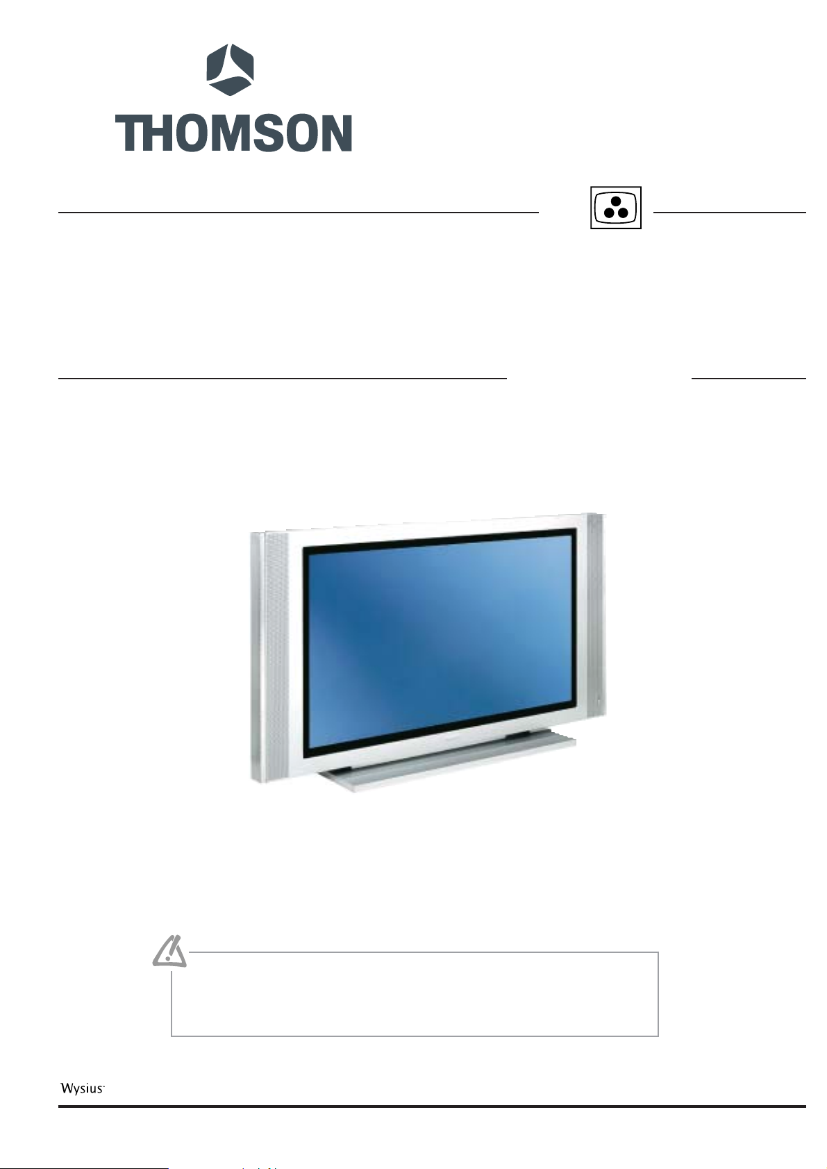
42WM03ST
42WM04ST
TV
Plasma
Page 2
Indicates critical safety components, and identical components should be used for replacement. Only then can the
operational safety be garanteed.
Le remplacement des éléments de sécurité (repérés avec le symbole ) par des composants non homologués selon la
Norme CEI 65 entraine la non-conformité de l'appareil. Dans ce cas, la responsabilité du fabricant n'est plus engagée.
Wenn Sicherheitsteile (mit dem Symbol gekennzeichnet) nicht durch Original - Ersatzteile ersetzt werden, erlischt die
Haftung des Herstellers.
La sostituzione dei componenti di sicurezza (evidenziati con il segno ) con componenti non omologati secondo la
norma CEI 65 comporta la non conformitá dell'apparecchio. In tal caso è "esclusa la responsabilità " del costruttore.
La sustitución de elementos de seguridad (marcados con el simbolo ) por componentes no homologados segun la
norma CEI 65, provoca la no conformidad del aparato. En ese caso, el fabricante cesa de ser responsable.
MEASUREMENT CONDITIONS - CONDITIONS DE MESURES - MESSBEDINGUNGEN
CONDIZIONI DI MISURA - CONDICIONES DE MEDIDAS
RICEVITORE :
In UHF, livello d'entrata 1 mV, monoscopio barre :
- PAL, norma G. bianco 100%.
Via SCART, livello d'entrata 1 Vpp, monoscopio barre :
Colore, Contrasto, Luminositá media, Suono minimo.
Programma selezionato PR 01.
Tensioni continue rilevate rispetto alla massa con un voltmetro digitale.
RECEIVER :
On UHF,input level : 1 mV, bar test pattern :
- PAL, I standard, 100% white.
Via the scart socket, input level : 1 Vpp, bar test pattern :
Colour, contrast and brightness at mid-position, sound at minimum.
Programme selected : PR 01.
DC voltages measured between the point and earth using a digital
voltmeter.
EMPFÄNGER :
Bei UHF Eingangspegel 1 mV, Farbbalken :
- PAL, Norm G, Weiss 100%.
Über die Scartbuchse : Eingangspegel 1 Vss, Farbbalken :
Farbe, Kontrast, Helligkeit in der Mitte des Bereichs, Ton auf Minimum.
Zugeordnetes Programm PR 01.
Gleichspannungen mit einem digitalen Voltmeter zur Masse gemessen.
RECEPTEUR :
En UHF, niveau d'entrée 1 mV mire de barres
- SECAM, Norm L, Blanc 100%.
Par la prise Péritélévision, niveau d'entrée 1 Vcc, mire de barres .
Couleur, contraste, lumière à mi-course, son minimum.
Programme affecté PR 01.
Tensions continues relevées par rapport à la masse avec un
voltmètre numérique.
RECEPTOR :
En UHF, nivel de entrada 1 mV, mira de barras :
- PAL, norma G, blanco 100%.
Por la toma Peritelevision, nivel de entrada 1 Vpp mira de barra.
Color, Contraste, luz a mitad de carrera, Sonido minimo.
Programa afectado PR 01.
Tensiones continuas marcadas en relacion a la masa con un voltimetro digital.
Do not disconnect modules when they are energized!
Repairs on power supply section are to be carried out only with isolating transformer.
Ne pas retirer les modules lorsqu' ils sont sous tension. N'effectuer les travaux de maintenance sur la partie reliée
au secteur (Switch Mode) qu'au travers d'un transformateur d'isolement.
Module nicht bei eingeschaltetem Gerät entfernen!
Servicearbeiten am Netzteil nur unter Verwendung eines Regeltrenntrafos durchführen.
Non scollegare le piastre quando sono alimentate!
Per le riparazioni sulla sezione alimentatore, utilizzare un trasformatore isolatore.
No desconectar los módulos cuando están activados. Las reparaciones en la sección de alimentación de energía
deben ser ejecutadas solamente con un transformador de separación.
Page 3

First issue 10 / 04 3
Page
SAFETY PRECAUTIONS . . . . . . . . . . . . . . . . . . . . . . . . . . . . . . . . . . . . . . . . . . . . . . . . . . . . . . . . . . 4
DISASSEMBLY
Removing the leg tube assembly . . . . . . . . . . . . . . . . . . . . . . . . . . . . . . . . . . . . . . . . . . . . . . . . .6
Removing the rear cover . . . . . . . . . . . . . . . . . . . . . . . . . . . . . . . . . . . . . . . . . . . . . . . . . . . . . . . . 7
Removing the filter . . . . . . . . . . . . . . . . . . . . . . . . . . . . . . . . . . . . . . . . . . . . . . . . . . . . . . . . . . . . . 8
TROUBLESHOOTING
No power . . . . . . . . . . . . . . . . . . . . . . . . . . . . . . . . . . . . . . . . . . . . . . . . . . . . . . . . . . . . . . . . . . .10
No picture . . . . . . . . . . . . . . . . . . . . . . . . . . . . . . . . . . . . . . . . . . . . . . . . . . . . . . . . . . . . . . . . . . . 11
Vertical line fail . . . . . . . . . . . . . . . . . . . . . . . . . . . . . . . . . . . . . . . . . . . . . . . . . . . . . . . . . . . . . . 12
Horizontal line fail . . . . . . . . . . . . . . . . . . . . . . . . . . . . . . . . . . . . . . . . . . . . . . . . . . . . . . . . . . . . 13
No command . . . . . . . . . . . . . . . . . . . . . . . . . . . . . . . . . . . . . . . . . . . . . . . . . . . . . . . . . . . . . . . . 14
ADJUSTMENTS
Power (PLG-421) . . . . . . . . . . . . . . . . . . . . . . . . . . . . . . . . . . . . . . . . . . . . . . . . . . . . . . . . . . . . . 15
Power (DGK-420W) . . . . . . . . . . . . . . . . . . . . . . . . . . . . . . . . . . . . . . . . . . . . . . . . . . . . . . . . . . . 16
Color temperature in DVI mode . . . . . . . . . . . . . . . . . . . . . . . . . . . . . . . . . . . . . . . . . . . . . . . . . .16
Color temperature in RGB mode . . . . . . . . . . . . . . . . . . . . . . . . . . . . . . . . . . . . . . . . . . . . . . . . . 18
SPECIFICATIONS . . . . . . . . . . . . . . . . . . . . . . . . . . . . . . . . . . . . . . . . . . . . . . . . . . . . . . . . . . . . . . . 20
APPENDIX A . . . . . . . . . . . . . . . . . . . . . . . . . . . . . . . . . . . . . . . . . . . . . . . . . . . . . . . . . . . . . . . . . . . .24
WIRING DIAGRAM . . . . . . . . . . . . . . . . . . . . . . . . . . . . . . . . . . . . . . . . . . . . . . . . . . . . . . . . . . . . . . .26
BLOCK DIAGRAM . . . . . . . . . . . . . . . . . . . . . . . . . . . . . . . . . . . . . . . . . . . . . . . . . . . . . . . . . . . . . . .27
SCHEMATIC DIAGRAMS
Tuner . . . . . . . . . . . . . . . . . . . . . . . . . . . . . . . . . . . . . . . . . . . . . . . . . . . . . . . . . . . . . . . . . . 28 - 32
Main . . . . . . . . . . . . . . . . . . . . . . . . . . . . . . . . . . . . . . . . . . . . . . . . . . . . . . . . . . . . . . . . . . 33 - 51
SPECIAL MODE . . . . . . . . . . . . . . . . . . . . . . . . . . . . . . . . . . . . . . . . . . . . . . . . . . . . . . . . . . . . . 52 - 53
EXPLODED VIEW . . . . . . . . . . . . . . . . . . . . . . . . . . . . . . . . . . . . . . . . . . . . . . . . . . . . . . . . . . . . . . . 54
CONTENTS
Page 4
4 First issue 10 /04
IMPORTANT SAFETY PRECAUTIONS
1. Before returning an instrument to the customer, always make a safety check of the entire instrument, including the
following items, but not limited to them.
a. Be sure that no built-in protective devices are defective and/or have been defeated during servicing. (1) Protective
shields are provided on this chassis to protect both the technician and the customer. Correctly replace all missing
protective shields, including any removed for servicing convenience. (2) When reinstalling the chassis and/or other
assembly in the cabinet, be sure to put back in place all protective devices, including, but not limited to, non-metallic
control knobs, insulating fishpapers, adjustment and compartment covers/shields, and isolation resistor/capacitor
networks. Do not operate this instrument or permit it to be operated without all protective devices correctly
installed and functioning.
b. Be sure that there are no cabinet openings through which an adult or child might be able to insert their fingers and
contact a hazardous voltage. Such opening include, but are not limited to (1) spacing between the picture tube and
the cabinet mask, (2) excessively wide cabinet ventilation slots, and (3) an improperly fitted and/or incorrectly
secured cabinet back cover.
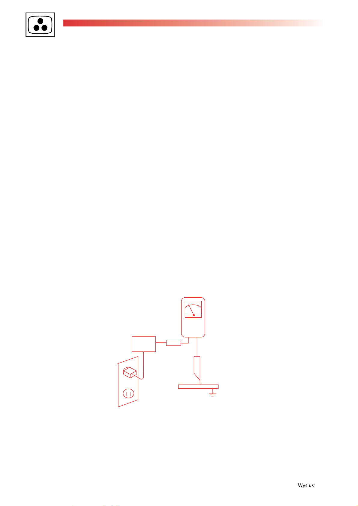
c. Leakage Current Hot Check: With the instrument completely reassembled, plug the AC line cord directly into a 230V
AC outlet. (Do not use an isolation transformer during this test.) Use a leakage current tester or a metering system.
With the instrument AC, first switch ON and then OFF. Measure from a known earth ground (metal waterpipe,
conduit, etc.) to all exposed metal parts of the instrument (antennas, handle bracket, metal cabinet, screwheads,
metallic overlays, control shafts, etc.), especially any exposed metal parts that offer an electrical return path to the
chassis. Any current measured must not exceed 3.5 mA. Reverse the instrument power cord plug in the outlet and
repeat test. ANY MEASUREMENTS NOT WITHIN THE LIMITS SPECIFIED HEREIN INDICATE A POTENTIAL
SHOCK HAZARD THAT MUST BE ELIMINATED BEFORE RETURNING THE INSTRUMENT TO THE
CUSTOMER.
2. Read and comply with all caution and safety-related notes on or inside the Monitor cabinet, on the Projection Monitor
chassis or on the picture tube.
+-
Test all exposed
metal surfaces
3. Wire cord
Also test with
plug reversed
(using AC adapter
plug as required)
Device
under
test
Earth ground
Leakage
current
tester
AC Leakage test
(Reading
should not
be above
3.5 mA)
Page 5

First issue 10 / 04 5
3. Design Alteration Warning: Do not alter or add to the mechanical or electrical design of this unit. Design alterations and
additions, including, but not limited to, circuit modifications and the addition of the items such as auxiliary audio and/or
video output connections might alter the safety characteristics of this Projection Monitor and create a hazard to the user.
Any design alterations or additions will void the manufacturer's warranty and will make you, the service, responsible for
personal injury or property damage resulting therefrom.
4. Hot Chassis Warning:
a. Some Monitor chassis are electrically connected directly to one conductor of the AC power cord and may be safely
serviced without an isolation transformer only if the AC power plug is inserted so that the chassis is connected to the
ground side of the AC power source. To confirm that the AC power plug is inserted correctly, with an AC voltmeter
measure between the chassis and a known earth ground. If a voltage reading in excess of 1.0V is obtained, remove
and reinsert the AC power plug in opposite polarity and again measure the voltage potential between the chassis
and a known earth ground.
b. Some Monitor chassis normally have 85V AC (RMS.), between chassis and earth ground regardless of the AC plug
polarity. These chassis can be safely serviced only with an isolation transformer inserted in the power line between
the receiver and the AC power source, for both personnel and test equipment protection.
c. Some Projection Monitor chassis have a secondary ground system in addition to the main chassis ground. This
secondary ground system is not isolated from the AC power line. Insulating material that must not be defeated or
altered electrically separates the two ground systems.
5. Observe original lead dress. Take extra care to assure correct lead dress in the following areas:
a. near sharp edges,
b. near thermally hot parts (be sure that leads and components do not touch thermally hot parts),
c. the AC supply,
d. high voltage,
e. antenna wiring. Always inspect in all areas for pinched, out-of-place, or frayed wiring. Do not change spacing
between components and between components and the printed-circuit board. Check AC powers cord for damage.
6. Components, parts, and/or wiring that appear to have overheated or are otherwise damaged should be replaced with
components, parts, or wiring that meet original specifications. Additionally, determine the cause of overheating and/or
damage and, if necessary, take corrective action to remove any potential safety hazard.
7. PRODUCT SAFETY NOTICE: Many Monitor electrical and mechanical parts have special safety-related characteristics
some of which are often not evident from visual inspection, nor can the protection they give necessarily be obtained by
replacing them with components rated for higher voltage, wattage, etc. Parts that have special safety characteristics are
identified in this service data by shading with a mark on schematics. Use of a substitute replacement part that does not
have the same safety characteristics as the recommended replacement part in this service data parts list might create
shock, fire, and/or other hazards.
Page 6
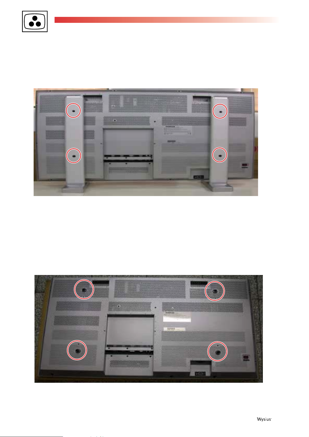
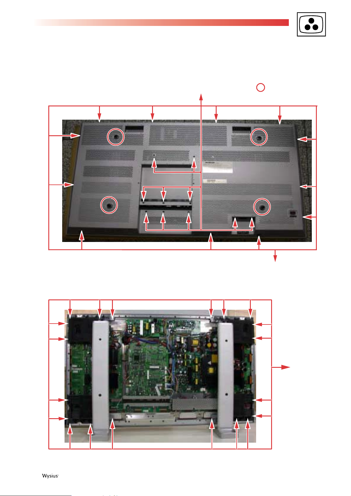
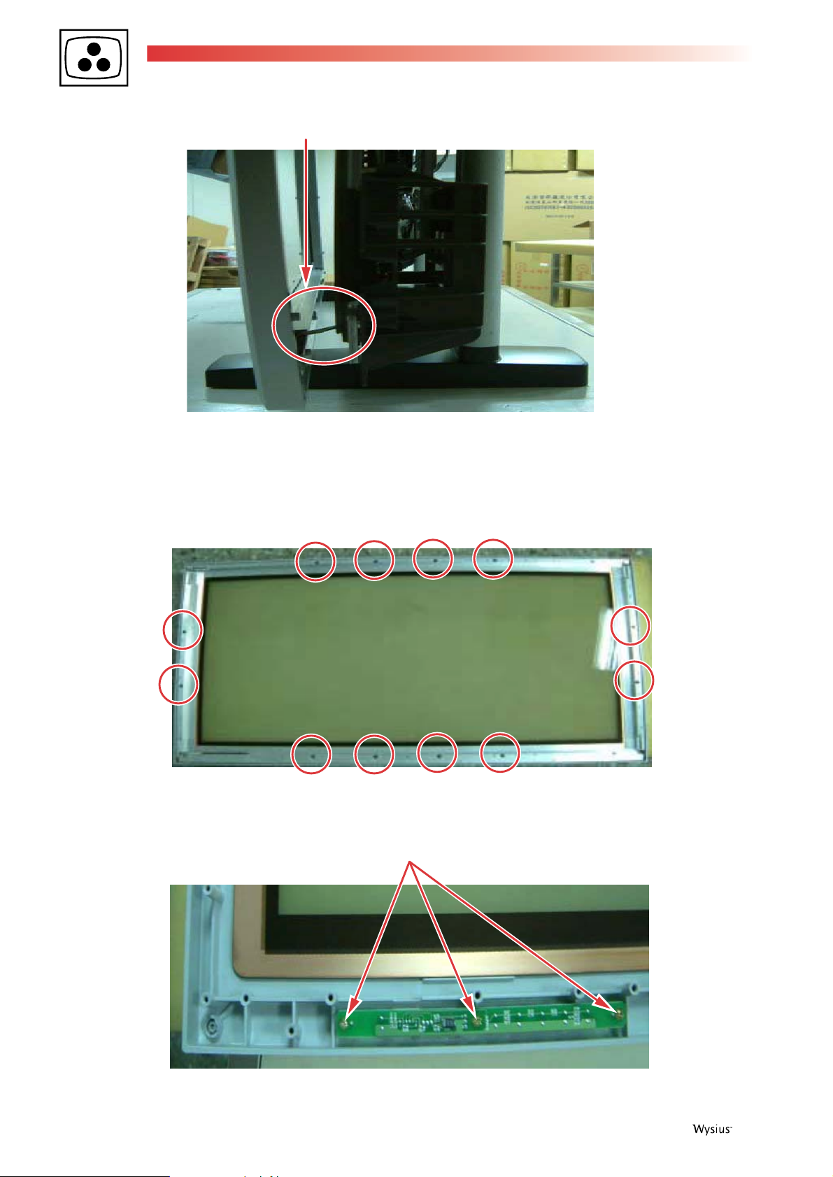
1. Removing the Leg Tube Assembly
Unscrew 4 screws from "Leg Tube Assembly." (Specification of screw driver is 15± 2kg), see fig.1
Push the "Leg Tube Assembly." downward to unlock and pull it away from unit, then unscrew 4 screws from rear cover.
(Specification of screw -driver is 15± 2 kg),
6 First issue 10 /04
Fig. 1
Fig. 2
HOW TO EXCHANGE THE MASK & PANEL PROCEDURE
Page 7
First issue 10 / 04 7
2. Removing the rear cover
Unscrew 12 screws from rear cover, see red arrow (Specification of screw driver is 15± 2 kg)
Unscrew 8 screws from rear cover, and unscrew 2 screws from AC power socket, see red arrow (Specification of screw driver
is 9± 1 kg)
Unscrew 4 screws from rear cover, see red circle (Specification of screw driver is 15± 2 kg)
3. Removing the screws from panel:
Unscrew 20 pieces of screw from panel site (Specification of screw driver is 15± 2 kg)
10 screws
12 screws
4 screws
Fig. 3
20 screws
Fig. 4
Page 8
8 First issue 10 /04
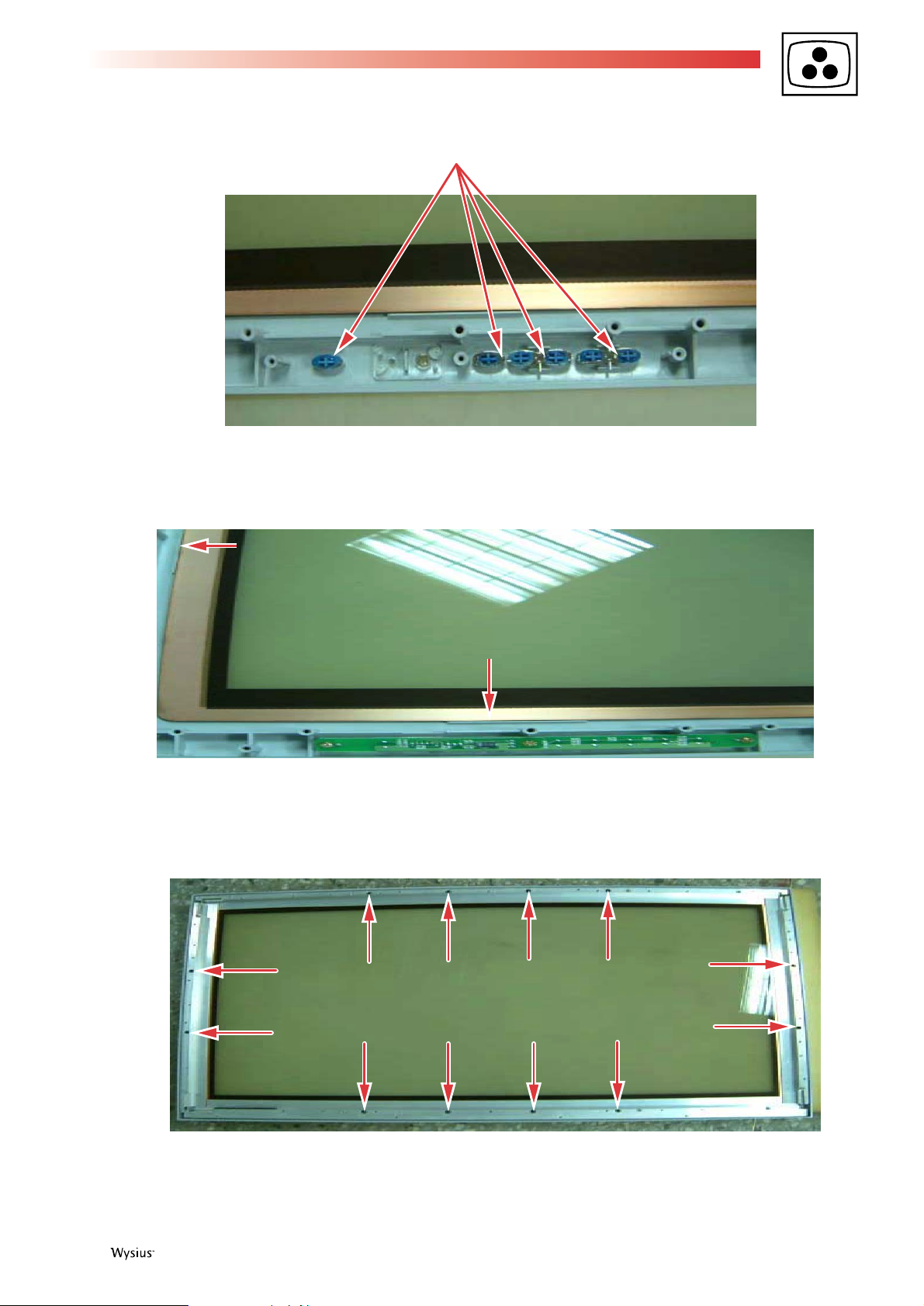
4. Removing the Mask and the J5 cable from PCB
5. Removing the filter
Unscrew 10 screws from mask (Specification of screw driver is 15± 2 kg), then remove four angles that hold the PDP filter. (Be
careful: Please do not bump or scrape when handling the PDP filter.)
Before putting panel back clean PDP filter make sure it's free from dust.
Unscrew 3 screws and remove control board
3 screws
Fig. 6
Fig. 7
J5
Fig. 5
Page 9
First issue 10 / 04 9
Remove the Control buttons from old Mask and reinstall them on the new Mask.
Please to aim at red arrow to guide and there is have a channel when you put down glass back to new mask
Assemble 4 irons back to mask. Be careful: When you lock up 4 irons that screws should be to lock up on "SL&G" point.
6. Proceed in reverse order to re-assemble
Control buttons
Fig. 8
Fig. 9
Top side
Top bottom
Fig. 10
Page 10
10 First issue 10 /04
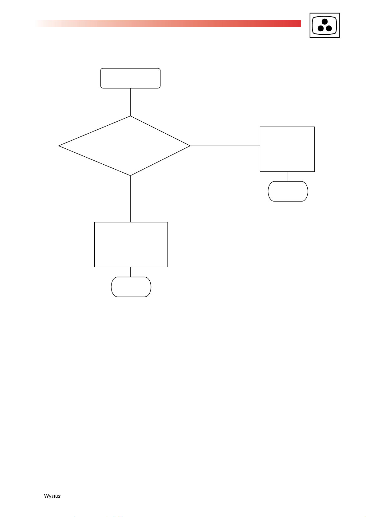
TROUBLESHOOTING
No power
Switch the
power on
Check "Power Switch" module
Not correct
Correct
Replace
"Power Switch"
module
Replace
"Main Power"
module
End
End
Page 11
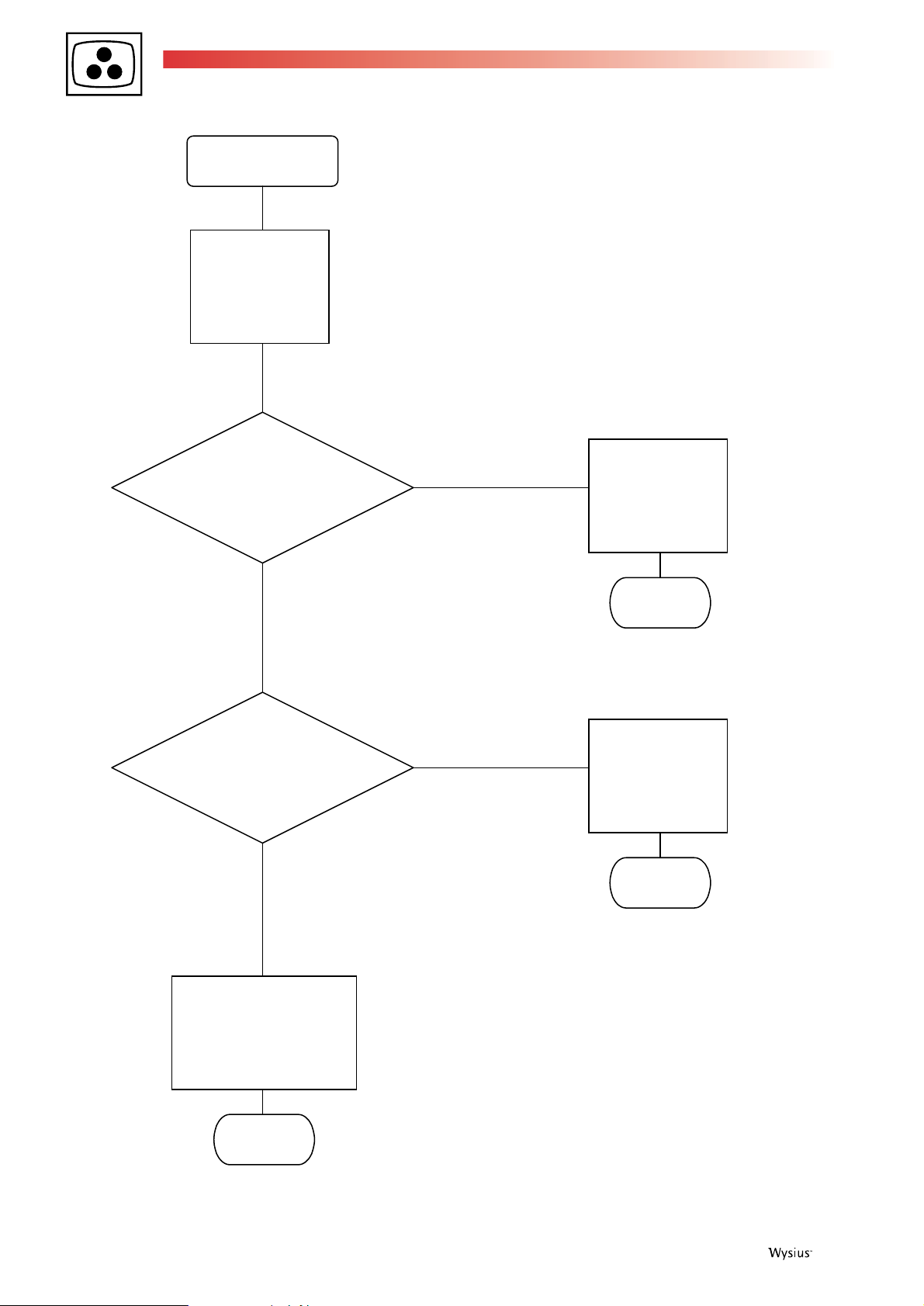
First issue 10 / 04 11
No picture
Check Image board
Not correct
Correct
Replace
Image board
Replace
PDP module
End
End
Page 12
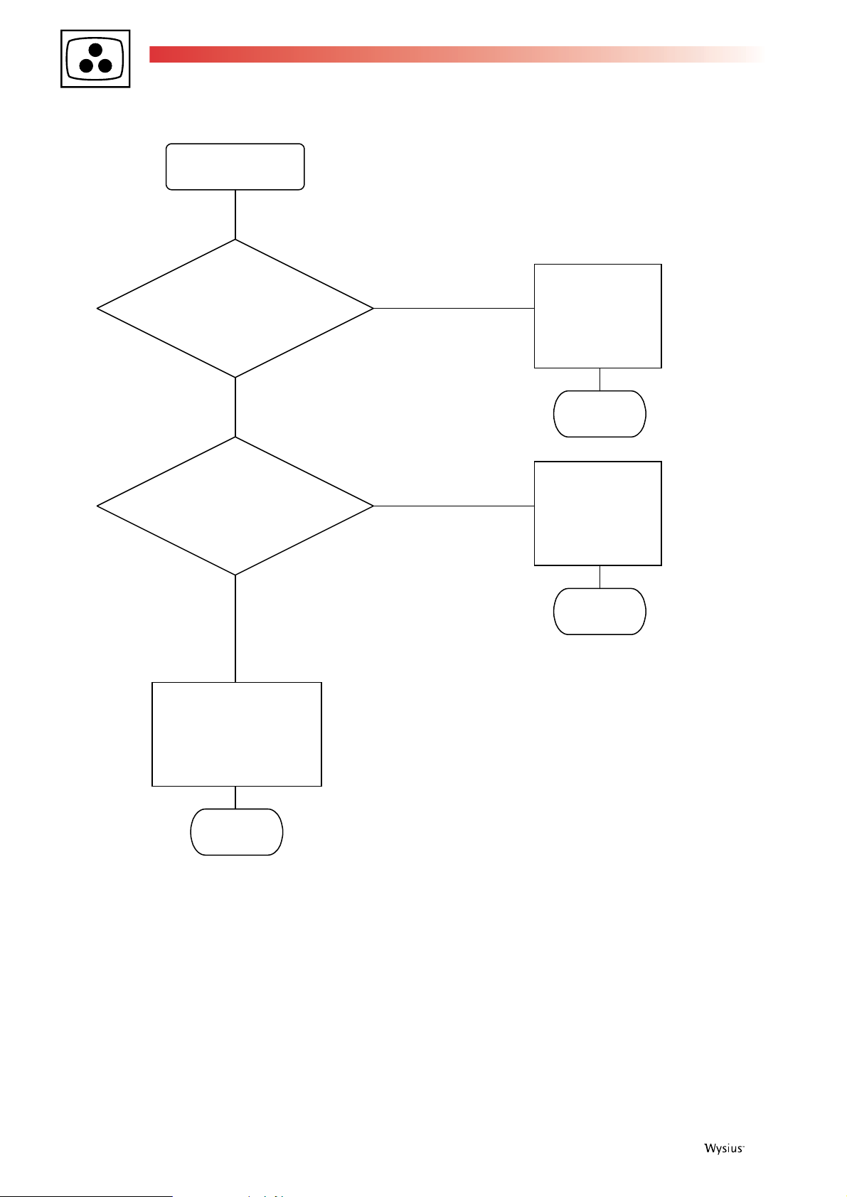
12 First issue 10 /04
Vertical line fail
Check XR Board
Check Logic Board
Not correct
Correct
Not correct
Correct
Replace
XR
Board
Replace
Logic
Board
Replace
PDP module
End
End
End
Page 13
First issue 10 / 04 13
Horizontal line fail
Check Y-SUS Board
Check Y DRV-Top
Not correct
Correct
Not correct
Correct
Replace
Y-SUS
Board
Replace
Y DRV-Top
Replace
PDP module
End
Check Z-SUS Board
Not correct
Correct
Replace
Z-SUS
Board
End
End
Check Y DRV-Bottom
Not correct
Correct
Replace Y
DRV-Bottom
End
End
Page 14
14 First issue 10 /04
No command
Switch the
power on
Check remote control
Check Front Button
Control Board
Not correct
Correct
Not correct
Correct
Replace the
battery or the
remote control
Replace
Front Button
Control Board
Replace Image
Board
End
End
End
Page 15
First issue 10 / 04 15
ADJUSTMENTS
PANEL voltage adjustment
1.1 Origin Power (PLG-421)
1. POWER ON
2. Signal Source: No (black screen).
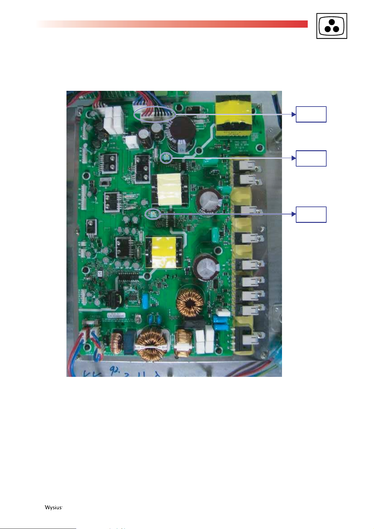
3. Connect Digital Voltage Meter (-) to Panel GND. Connect Digital Voltage Meter (+) to Plug CN806 Pin#10 and adjust the VA
(Variable Resistor RV204) value to the VA value recorded on the Panel Voltage Label ±0.5VDC (VA ± 0.5VDC= value adjusted).
4. Connect Digital Voltage Meter (-) to Panel GND. Connect Digital Voltage Meter (+) to Plug CN806 Pin#1 and adjust the VS
(Variable Resistor RV203) value to the VS value recorded on the Panel Voltage Label ±0.5VDC (VS ± 0.5VDC= value adjusted).
Remark: The Panel Voltage Label is located at the upper- right corner of the panel.
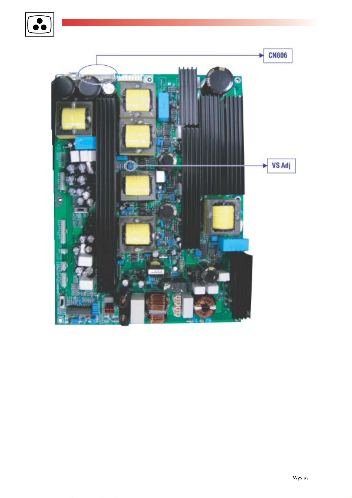
CN806
RV203
RV204
Page 16
16 First issue 10 /04
1.2 Dae Gil Power (DGK-420W)
1. POWER ON
2. Signal Source: No (black screen).
3. Connect Digital Voltage Meter (-) to Panel GND. Connect Digital Voltage Meter (+) to Plug CN806 Pin#10 and adjust the VA
(Variable Resistor) value to the VA value recorded on the Panel Voltage Label ± 0.5VDC (VA ± 0.5VDC= value adjusted).
4. Connect Digital Voltage Meter (-) to Panel GND. Connect Digital Voltage Meter (+) to Plug CN806 Pin#1 and adjust the VS
(Variable Resistor) value to the VS value recorded on the Panel Voltage Label ± 0.5VDC (VS ± 0.5VDC= value adjusted).
Remark: The Panel Voltage Label is located at the upper-right corner of the panel.
Color Temperature Adjustment
1.1 Color Temperature setting in DVI Mode
1. Turn on PDP set and warm up for over 30 minutes.
Page 17
First issue 10 / 04 17
2. Turn on Color Analyzer CA-100 and reset CA-100.
3. Switch PDP input signal source to DVI mode.
4. Set up Video Pattern Generator (Astro, Model= VG-828H).
Timing set = 640 x 480 @ 60Hz;
Video = Panel Link (the DVI output mode)
Connect PDP DVI input connector with Astro to receive DVI signal.
5. Dark level and bright level center block definition:
A. Dark level center block definition:
[WINDOW]
Mode %
Format 1 Window
Flicker None
Size H/V 28.5/34.0 (%)
Analog R/G/B 25/25/25 (10 IRE white output pattern)
B. Bright level center block definition:
[WINDOW]
Mode %
Format 1 Window
Flicker None
Size H/V 28.5/34.0 (%)
Analog R/G/B 153/153/153 (60 IRE white output pattern)
6. There are 4 different modes (DVI / RGB / AV / YPBPR) color temperature setting; there are 3 different color temperatures
(7180K, 8680K and 10180K) in each mode. Each color temperature needs to adjust dark
level, bright level, and R, G, B.
The OSD menu for color temperature factory setting can be viewed by following the ”Factory Setting Procedure”.
Factory Setting Procedure:
A. Press (Zoom -) key for over 5 seconds and release.
B. Press (Zoom+) key for over 5 seconds and release.
C. Press ”ok” key.
D. Factory setting OSD menu shows up. The values shown up on the OSD menu are the factory default setting values.
The factory default setting values differ from each PDP panel module. The color temperature factory setting OSD menus
are as the following:
*Note: When adjusting the color temperature, please note
what is the input source and what input the PDP is, the input
source and the PDP input mode should be the same.
7. Put the color analyzer CA-100 in the center of the screen.
A. 7180K
DV I -CT : 718 0
K
[x : 3 0 8 y : 2 9 8]
GA IN B IAS
RG B RG B
xx xx xx xx xx xx
xx xx
B. 8680K
DV I -CT : 868 0
o
K
[x : 2 8 8 y : 3 0 1]
GA IN B IAS
RG B RG B
xx xx xx xx xx xx
xx xx
C. 10180K
DV I -CT :10180
o
K
[x : 2 7 0 y : 2 9 2]
GA IN B IAS
RG B RG B
xx xx xx xx xx xx
xx xx
(GAIN Gamma) (BIAS Gamma)
Page 18

18 First issue 10 /04
1.2 Adjusting procedure
1. Receive Astro VG-828H DVI dark level center block signal (14 IRE), follow the ”Factory Setting Procedure” to go into
factory setting mode and you will see the 7180K color temperature setting OSD menu.
2. 7180K dark level center block adjustment procedure:
A. Press (Zoom -) or (Zoom+) key in remote control to select G-BIAS, and adjust Y=0.4 FL±0.1FL
B. Press(Zoom -) or (Zoom+) key in remote control to select R-BIAS, and adjust x=308±15FL
C. Press (Zoom -) or (Zoom+) key in remote control to select B-BIAS, and adjust y=298±15FL
D. Adjust R/G/B-BIAS, make sure the final value x=308±15FL, y=298±15FL, Y=0.4FL±0.1FL
3. 7180K bright level center block adjustment procedure:
(Please set Astro VG-828H DVI bright level center block signal to 60 IRE)
A. Press (Zoom -) or (Zoom+) key in remote control to select G-GAIN, and adjust Y=40±2FL
B. Press (Zoom -) or (Zoom+) key in remote control to select R-GAIN, and adjust x=308±15FL
C. Press (Zoom -) or (Zoom+) key in remote control to select B-GAIN, and adjust y=298±15F
D. Adjust R/G/B-GAIN, make sure the final value x=308±15FL, y=298±15FL, Y=40±2FL.
E. Press (Zoom+) key in remote control to select GAIN Gamma, and then press (Zoom -) or (Zoom+) key to adjust to Y=40
F. Press (Zoom+) key in remote control to select BIAS Gamma, and then press (Zoom -) or (Zoom+) key to adjust to Y=0.4
4. When you want to go ahead for next color temperature setting, double check the Gamma values, make sure GAIN
Gamma and BIAS Gamma values are correct, and then press the ”ok” key in remote control. For each color temperature
setting, please repeat the procedure (1)-(3). Only x and y value will change in different color temperature mode (in 8680K,
x=288, y=301; in 10180K, x=270, y=292) and Y values are all the same in each color temperature mode (dark level Y=0.4,
bright level Y=40).
2.1 Color Temperature setting in RGB Mode
1. Turn on Color Analyzer CA-100 and reset CA-100.
2. Switch PDP input signal source to RGB mode.
3. Set up Video Pattern Generator (Astro, Model= VG-828H).
Timing set = 640 x 480 @ 60Hz;
Video = Analog (the RGB output mode)
Connect PDP RGB input connector with Astro to receive RGB signal.
4. Dark level and bright level center block definition:
A. Dark level center block definition:
[WINDOW]
Mode %
Format 1 Window
Flicker None
Size H/V 28.5/34.0 (%)
Analog R/G/B 25/25/25 (10 IRE white output pattern)
B. Bright level center block definition:
[WINDOW]
Mode %
Format 1 Window
Flicker None
Size H/V 28.5/34.0 (%)
Analog R/G/B 153/153/153 (60 IRE white output pattern)
5. There are 4 different modes (DVI / RGB / AV / YPBPR) need color temperature setting; there are 3 different color
temperatures (7180K, 8680K and 10180K) in each mode. Each color temperature needs to adjust dark level, bright level,
and R, G, B. The OSD menu for color temperature factory setting can be viewed by following the ”Factory Setting Procedure”.
Page 19

First issue 10 / 04 19
Factory Setting Procedure:
A. Press (Zoom -) key for over 5 seconds and release.
B. Press (Zoom+) key for over 5 seconds and release.
C. Press ”ok” key.
D. Factory setting OSD menu shows up.
The values showed up on the OSD menu are the factory default setting values. The factory default setting values differ from
each PDP panel module. The color temperature factory setting OSD menus are as the following:
*Note: GAIN Gamma and BIAS Gamma have no function
under RGB mode.
*Note: When adjusting the color temperature, please note
what is the input source and what input the PDP is, the
input source and the PDP input mode should be the same.
6. Put the color analyzer CA-100 in the center of the screen.
2.2 Adjusting procedure:
1. Receive Astro VG-828H RGB dark level center block signal (14 IRE), follow the ”Factory Setting Procedure” to go into
factory setting mode and you will see the 7180K color temperature setting OSD menu.
2. 7180K dark level center block adjustment procedure:
A. Press (Zoom -) or (Zoom+) key in remote control to select G-BIAS, and adjust Y=0.5 FL±0.1FL
B. Press (Zoom -) or (Zoom+) key in remote control to select R-BIAS, and adjust x=308±15FL
C. Press (Zoom -) or (Zoom+) key in remote control to select B-BIAS, and adjust y=298±15FL
D. Adjust R/G/B-BIAS, make sure the final value x=308±15FL, y=298±15FL, Y=0.5FL±0.1FL
3. 7180K bright level center block adjustment procedure:
(Please set Astro VG-828H RGB bright level center block signal to 60 IRE)
A. Press (Zoom -) or (Zoom+) key in remote control to select G-GAIN, and adjust Y=40±2FL
B. Press (Zoom -) or (Zoom+) key in remote control to select R-GAIN, and adjust x=308±15FL
C. Press (Zoom -) or (Zoom+) key in remote control to select B-GAIN, and adjust y=298±15F
D. Adjust R/G/B-GAIN, make sure the final value x=308±15FL, y=298±15FL, Y=40±2FL.
4. When you want to go ahead for next color temperature setting, double check the Gamma values, make sure GAIN Gamma
and BIAS Gamma values are correct, and then press the ”ok” key in remote control. For each color temperature setting,
please repeat the procedure (1)-(3). Only x and y value will change in different color temperature mode (in 8680K, x=288,
y=301; in 10180K, x=270, y=292) and Y values are all the same in each color temperature mode (dark level Y=0. 5, bright
level Y=40).
3.1 Color Temperature setting in AV Mode
1. Turn on Color Analyzer CA-100 and reset CA-100.
A. 7180K
o
RGB -CT : 7 1 8 0
[x : 3 08 y :298]
GA IN B IAS
RG B RG B
xx xx Xx xx xx xx
K
xx xx
B. 8680K
RGB -CT : 8 6 8 0
[x : 2 88 y :301]
GA IN B IAS
RG B R
Xx xx Xx xx xx xx
xx xx
K
RGB-CT: 1
[x : 2 70 y :
GA IN B
RG B RGB
xx xx xx x xx xx
xx xx
0180
:292]
IAS
GB
o
(GAIN Gamma) (BIAS Gamma)
C. 10180K
o
K
Page 20

20 First issue 10 /04
2. Switch PDP input signal source to AV mode.
3. Set up Video Pattern Generator (Astro, Model= VG-828H).
Timing set = 640 x 480 @ 60Hz;
Video = Analog (the AV output mode)
Connect PDP AV input connector with Astro to receive AV signal.
4. Dark level and bright level center block definition:
A. Dark level center block definition:
[WINDOW]
Mode %
Format 1 Window
Flicker None
Size H/V 28.5/34.0 (%)
Analog R/G/B 25/25/25 (10 IRE white output pattern)
B. Bright level center block definition:
[WINDOW]
Mode %
Format 1 Window
Flicker None
Size H/V 28.5/34.0 (%)
Analog R/G/B 153/153/153 (60 IRE white output pattern)
5. There are 4 different modes (DVI / RGB / AV / YPBPR) need color temperature setting; there are 3 different color
temperatures (7180K, 8680K and 10180K) in each mode. Each color temperature needs to adjust dark level, bright level,
and R, G, B. The OSD menu for color temperature factory setting can be viewed by following the ”Factory Setting Procedure”.
Factory Setting Procedure:
A. Press (Zoom -) key for over 5 seconds and release.
B. Press (Zoom+) key for over 5 seconds and release.
C. Press ”ok” key.
D. Factory setting OSD menu shows up.
The values showed up on the OSD menu are the factory default setting values. The factory default setting values differ from
each PDP panel module.
6. Put the color analyzer CA-100 in the center of the screen.
3.2 Adjusting procedure:
1. Receive Astro VG-828H AV dark level center block signal (14 IRE), follow the ”Factory Setting Procedure” to go into
factory setting mode and you will see the 7180K color temperature setting OSD menu.
2. 7180K dark level center block adjustment procedure:
A. Press (Zoom -) or (Zoom+) key in remote control to select G-BIAS, and adjust Y=1.0 FL±0.1FL
B. Press (Zoom -) or (Zoom+) key in remote control to select R-BIAS, and adjust x=308±15FL
C. Press (Zoom -) or (Zoom+) key in remote control to select B-BIAS, and adjust y=298±15FL
D. Adjust R/G/B-BIAS, make sure the final value x=308±15FL, y=298±15FL, Y=1.0FL±0.1FL
3. 7180K bright level center block adjustment procedure:
(Please set Astro VG-828H RGB bright level center block signal to 60 IRE)
A. Press (Zoom -) or (Zoom+) key in remote control to select G-GAIN, and adjust Y=40±2FL
B. Press (Zoom -) or (Zoom+) key in remote control to select R-GAIN, and adjust x=308±15FL
C. Press (Zoom -) or (Zoom+) key in remote control to select B-GAIN, and adjust y=298±15F
D. Adjust R/G/B-GAIN, make sure the final value x=308±15FL, y=298±15FL, Y=40±2FL.
4. When you want to go ahead for next color temperature setting, double check the Gamma values, make sure GAIN Gamma
Page 21

First issue 10 / 04 21
and BIAS Gamma values are correct, and then press the ”ok” key in remote control. For each color temperature setting,
please repeat the procedure (1)-(3). Only x and y value will change in different color temperature mode (in 8680K, x=288,
y=301; in 10180K, x=270, y=292) and Y values are all the same in each color temperature mode (dark level Y=1.0, bright
level Y=40).
4 .1 Color Temperature setting in YPBPR Mode
1. Turn on Color Analyzer CA-100 and reset CA-100.
2. Switch PDP input signal source to YPBPR mode.
3. Set up Video Pattern Generator (Astro, Model= VG-828H).
Timing set = 640 x 480 @ 60Hz;
Video = Analog (the YPBPR output mode)
Connect PDP YPBPR input connector with Astro to receive YPBPR signal.
4. Dark level and bright level center block definition:
A. Dark level center block definition:
[WINDOW]
Mode %
Format 1 Window
Flicker None
Size H/V 28.5/34.0 (%)
Analog R/G/B 25/25/25 (10 IRE white output pattern)
B. Bright level center block definition:
[WINDOW]
Mode %
Format 1 Window
Flicker None
Size H/V 28.5/34.0 (%)
Analog R/G/B 153/153/153 (60 IRE white output pattern)
5. There are 4 different modes (DVI / RGB / AV / YPBPR) need color temperature setting; there are 3 different color
temperatures (7180K, 8680K and 10180K) in each mode. Each color temperature needs to adjust dark level, bright level,
and R, G, B. The OSD menu for color temperature factory setting can be viewed by following the ”Factory Setting Procedure”.
Factory Setting Procedure:
A. Press (Zoom -) key for over 5 seconds and release.
B. Press (Zoom+) key for over 5 seconds and release.
C. Press ”ok” key.
D. Factory setting OSD menu shows up.
The values showed up on the OSD menu are the factory default setting values. The factory default setting values differ from
each PDP panel module.
6. Put the color analyzer CA-100 in the center of the screen.
4.2 Adjusting procedure:
1. Receive Astro VG-828H YPBPR dark level center block signal (14 IRE), follow the ”Factory Setting Procedure” to go into
factory setting mode and you will see the 7180K color temperature setting OSD menu.
2. 7180K dark level center block adjustment procedure:
A. Press (Zoom -) or (Zoom+) key in remote control to select G-BIAS, and adjust Y=1.1 FL±0.1FL
B. Press (Zoom -) or (Zoom+) key in remote control to select R-BIAS, and adjust x=308±15FL
C. Press (Zoom -) or (Zoom+) key in remote control to select B-BIAS, and adjust y=298±15FL
D. Adjust R/G/B-BIAS, make sure the final value x=308±15FL, y=298±15FL, Y=1.1 FL±0.1FL
Page 22

22 First issue 10 /04
3. 7180K bright level center block adjustment procedure:
(Please set Astro VG-828H RGB bright level center block signal to 60 IRE)
A. Press (Zoom -) or (Zoom+) key in remote control to select G-GAIN, and adjust Y=41±2FL
B. Press (Zoom -) or (Zoom+) key in remote control to select R-GAIN, and adjust x=308±15FL
C. Press (Zoom -) or (Zoom+) key in remote control to select B-GAIN, and adjust y=298±15F
D. Adjust R/G/B-GAIN, make sure the final value x=308±15FL, y=298±15FL, Y=41±2FL.
4. When you want to go ahead for next color temperature setting, double check the Gamma values, make sure GAIN Gamma
and BIAS Gamma values are correct, and then press the ”ok” key in remote control. For each color temperature setting,
please repeat the procedure (1)-(3). Only x and y value will change in different color temperature mode (in 8680K, x=288,
y=301; in 10180K, x=270, y=292) and Y values are all the same in each color temperature mode (dark level Y=1.1, bright
level Y=41).
SPECIFICATIONS
Pin assignments
D-SUB Connector
DVI-Connector
1
15
9
15
824
610
11 15
Pin Pin PinSignal Signal Signal
Pin Pin PinSignal Signal Signal
1
2
3
4
5
RED
GREEN
BLUE
GND
GND
RED GND
GREEN GND
BLUE GND
NC
GND
GND
SDA
H_SYNC
V_SYNC
SCL
6
7
8
9
10
11
12
13
14
15
1
2
3
4
5
6
7
8
TMDS Data 2-
TMDS Data 2+
TMDS Data
2/4Shield
TMDS Data 4-
TMDS Data 4+
DDC Clock
DDC Data
NC
TMDS Data 0-
TMDS Data 0+
TMDS Data
0/5 Shield
TMDS Data 5-
TMDS Data 5+
TMDS Clock
Shield
TMDS Clock+
TMDS Clock-
TMDS Data 1-
TMDS Data 1+
TMDS Data
1/3 Shield
TMDS Data 3-
TMDS Data 3+
+5V Power
GND (for +5V)
Hot Plug
Detect
9
10
11
12
13
14
15
16
17
18
19
20
21
22
23
24
Page 23

First issue 10 / 04 23
Mode list for RGB / DVI
Note: 1. * : DVI is not supported.
2. Mode 24 to 26 are for use with Apple Macintosh computers.
Y/PB/PR for component
Refresh Horizontal Vertical Vertical Horizontal
Mode No Resolution Rate Frequency Frequency Sync Sync Dot rate
Polarity Polarity
(Hz) (K Hz) (Hz) (TTL) (TTL) (MHz)
1 640(VGA)x480 60 31.5 59.94 - - 25.175
2 640(VGA)x480 72 37.9 72.81 - - 31.500
3 640(VGA)x480 75 37.5 75 - - 31.500
4 640(VGA)x480 85 43.3 85.01 - - 36.000
5 800(SVGA)x600 56 35.1 56.25 + + 36.000
6 800(SVGA)x600 60 37.9 60.317 + + 40.000
7 800(SVGA)x600 72 48.1 72.19 + + 50.000
8 800(SVGA)x600 75 46.9 75 + + 49.500
9 800(SVGA)x600 85 53.7 85.06 + + 56.250
10 1024(XGA)x768 60 48.4 60.01 - - 65.000
11 1024(XGA)x768 70 56.5 70.07 - - 75.000
12 1024(XGA)x768 75 60.0 75.03 + + 78.750
13 1024(XGA)x768 85 68.7 84.99 + + 94.500
14 1280(SXGA)x1024 60 63.98 60.02 + + 108.00
15* 1280(SXGA)x1024 75 79.98 75.03 + + 135.00
16* 1280(SXGA)x1024 85 91.15 85.02 + + 157.50
18 720(DOS)x400 70 31.46 70.08 + - 28.320
19 640(VGA)x480 50 31.5 50 - - 25.175
20* 1280(HDTV)x720P 60 45.15 60 - - 74.250
21* 1920(HDTV)x1080I 60(I) 33.75 60 - - 74.250
22 640(VGA)x350 70 31.50 70 - + 25.175
23 852(WGA)x480 60 31.413 59.835 - - 30.00
24 640x480 67 35.00 66.67 - - 30.240
25 832 x 624 75 49.73 74.55 - - 57.283
26 1152 x 870 75 68.68 75.06 - - 100.000
Mode No Resolution Refresh Rate
1 640x480P 60 Hz
2 1920x1080I 60 Hz
3 1280x720P 60 Hz
4 720x576P 50 Hz
5 1920x1080I 50 Hz
6 1280x720P 50 Hz
Page 24

24 First issue 10 /04
APPENDIX A : Preset Timing Chart
Item Description:
A Total time
B Active display area including borders
C Active display area excluding borders
D Left/Top border
E Right/bottom border
F Blanking time
G Front porch
H Sync -width
I Back porch
Mode No 1 2 3 4 5 6 7 8 9
Resolution
&
Refresh Rate
Pixel clock 25.175 31.5 31.5 36 36 40 50 49.5 56.25 MHz
Horizontal visible 640 640 640 640 800 800 800 800 800 Dots
Horizontal total 800 832 840 832 1024 1056 1040 1056 1048 Dots
Horizontal front porch 16 24 16 56 24 40 56 16 32 Dots
Horizontal sync 96 40 64 56 72 128 120 80 64 Dots
Horizontal back porch 48 128 120 80 128 88 64 160 152 Dots
Horiz blanking time 160 192 200 192 224 256 240 256 248 Dots
Vertical visible 480 480 480 480 600 600 600 600 600 Lines
Vertical total 525 520 500 509 625 628 666 625 631 Lines
Vertical front porch 10 9 1 1 1 1 37 1 1 Lines
Vertical sync 2 3 3 3 2 4 6 3 3 Lines
Vertical back porch 33 28 16 25 22 23 23 21 27 Lines
Vertical blanking time 45 40 20 29 25 28 66 25 31 Lines
Horizontal frequency 31.469 37.861 37.5 43.269 35.156 37.879 48.077 46.875 53.674 kHz
Vertical frequency 59.94 72.809 75 85.008 56.25 60.317 72.188 75 85.061 Hz
Vertical sync polarity - - - - + + + + + TTL
Horiz sync polarity - - - - + + + + + TTL
640
480
60
640
480
72
640
480
75
640
480
85
800
600
56
800
600
60
800
600
72
800
600
75
800
600
85
Hz
Page 25

First issue 10 / 04 25
Mode No 10 11 12 13 14 15 16 18 19
Resolution
&
Refresh Rate
1024
768
60
1024
768
70
1024
768
75
1024
768
85
1280
1024
60
1280
1024
75
1280
1024
85
720
400
70
640
480
50 Hz
Pixel clock 65 75 78.75 94.5 108 135 157.5 28.320 25.175 MHz
Horizontal visible 1024 1024 1024 1024 1280 1280 1280 720 640 Dots
Horizontal total 1344 1328 1312 1376 1688 1688 1728 900 800 Dots
Horizontal front porch 24 24 16 48 48 16 64 18 16 Dots
Horizontal sync 136 136 96 96 112 144 160 108 96 Dots
Horizontal back porch 160 144 176 208 248 248 224 54 48 Dots
Horiz blanking time 320 304 288 352 408 408 448 180 160 Dots
Vertical visible 768 768 768 768 1024 1024 1024 400 480 Lines
Vertical total 806 806 800 808 1066 1066 1072 449 629 Lines
Vertical front porch 3 3 1 1 1 1 1 12 62 Lines
Vertical sync 6 6 3 3 3 3 3 2 2 Lines
Vertical back porch 29 29 28 36 38 38 44 35 85 Lines
Vertical blanking time 38 38 32 40 42 42 48 49 149 Lines
Horizontal frequency 48.364 56.476 60.023 68.677 63.981 79.976 91.146 31.469 31.469 kHz
Vertical frequency 60.004 70.069 75.029 84.997 60.020 75.025 85.024 70.087 50.030 Hz
Vertical sync polarity - - + + + + + + - TTL
Horiz sync polarity - - + + + + + - - TTL
Mode No 20 21 22 23 24 25 26
Resolution
&
Refresh Rate
1280
720P
60
1920
1080I
60I
640
350
70
852
480
60
640
480
67
832
624
75
1152
870
75
Hz
Pixel clock 74.250 74.25 25.175 30 30.24 57.283 100.000 MHz
Horizontal visible 1280 1920 640 852 640 832 1152 Dots
Horizontal total 1650 2200 800 955 864 1152 1456 Dots
Horizontal front porch 110 88 16 19 64 32 32 Dots
Horizontal sync 40 44 96 48 64 64 128 Dots
Horizontal back porch 220 148 48 36 96 224 144 Dots
Horiz blanking time 370 280 160 103 224 320 304 Dots
Vertical visible 720 540 350 480 480 624 870 Lines
Vertical total 750 562.5 449 525 525 667 915 Lines
Vertical front porch 5 3 37 10 3 1 3 Lines
Vertical sync 5 5 2 2 3 3 3 Lines
Vertical back porch 20 15 60 33 39 39 39 Lines
Vertical blanking time 30 23 99 45 45 43 45 Lines
Horizontal frequency 45.000 33.750 31.469 31.414 35.000 49.725 68.681 kHz
Vertical frequency 60 60 70.087 59.835 66.667 74.55 75.062 Hz
Vertical sync polarity - - - - - - - TTL
Horiz sync polarity - - + - - - - TTL
Page 26

First issue 06 / 04 26
WIRING DIAGRAM
PDP Module
AV Module
Board(with
Tuner)
Assy
JP2
Front
Button
Control
Board
Assy
JP1
JA3
Y DRV_TOP
Y DRV_BOTTOM
Y-SUS
Audio
Amplifier
Board Ass'y
(TMDS)
J1
JP4
JP5
J15
(9V)
J25
(5V)
JA2
JA1
Image Board
Ass'y
J14
(5V,SB DET)
J21
(24V,9V)
J28
(RLYON VSON)
J12
(Audio Signal)
J11
(Audio DC,Supply)
(Key)
CN803
CN802/CN809
Main Power
CN801
J5
AC_IN
CN02
CN03
Z-SUS
P21
Logic Board
AC Filter
Power
SW
AC IN
XR BOARD
Page 27

27 First issue 10 / 04
BLOCK DIAGRAM
TUNER
SCART
S-VIDEO
Connecter
Component
Connecter
TU1
Tuner Board Signal Block Diagram
COMPOSITE(AV)
TDA9181
Comb filter
ICT6
TV_CVBS
FB
R
G
B
Philips
UOC
ICT5
Y
C
CVBSO
R
G
B
VDRA
HOUT
for SUB-picture
74HC4053
ICT11
Monostable
Multivibrator
74HC4538
Monostable
Multivibrator
Y1
PB1_CB1
PR1_CR1
74HC211
ICT8
ICT9
R
G
B
H
V
S-VIDEO
TV_CVBS
COMPOSITE(AV)
TA1287P
RGB TO
YUV
ICT7
(48 Pin) (48 Pin)
Y2
CB2
CR2
JPT1
(48 Pin)
JPT1
(48 Pin)
JP4JPT1
S-VIDEO
TV_CVBS
COMPOSITE(AV)
IC3
CON1
CON2
CON3
JP4
(48 Pin)
Y2
CB2
CR2
JP4
(48 Pin)
Y1
PB1_CB1
PR1_CR1
MAIN Board Signal Block Diagram
Y
AV
IC1
MULTIPLEX
SWITCH
MULTIPLEX
SWITCH
IC7
CON1
CON2
CON3
IC3
IC7
C
VIDEO
Y
C
L
TA8551CH
SWITCH
LH
COMP.UOC
SDRAM
U48,49
6630/6730
MAIN Video
YCBCR
YCBCR
(480P720P1080I)
CON1
CON2 Trident
CON3
H
UOCCOMP.
Processor
6630/6730
SUB Video
Porcessor
YPBPR
L
COMP.
I/P
U45
U46
SDRAM
U50,51
MULTIPLEX
HIC2
Color Space
YP BPR(DOUBLE SCAN)
SWITCH
IC2
TA1276
Conveter
U43
RGB I/P
Connector
MULTIPLEX
SWITCH
U34
R,G,B
CPU
U4
RGB O/P
Connector
Converter
AD
U29
SIL161 DVI
U32
SDRAM
U25,26,27
SCALE IC
C711/C713
U23
Clock
Generator
9161A(PLL)
LVDS
TRANSMITTER
P
A
N
E
L
RS232
Connector
DVI IN
Page 28

First issue 10 / 04 28
TUNER BOARD SCHEMATIC DIAGRAM: TUNER & MSP
P9V
TU1
FQ1216MEIH3
ANT IN
VIDEO
5V IF
SOUND_IN _LP[2]
SOUND_IN _RP[2]
T
CT191
0.1uF
25V
Z
S2_LP[2]
S2_RP[2]
+
CT8
+
100uF
16V
CT17
0.01uF
50V
CT51
100uF
16V
PLT3
AF
+
RT47
0
1/16W
CT60
5PF
50V
D
CT67
5PF
50V
D
SB5V_CPU
CT188
0.1uF
25V
Z
D
SC L2P[3,5]
SDA2P[3,5]
CT58
33PF
50V
NCNC5V
1234567
CT18
100PF
50V
RT27
100
1/16W
CT36
1000PF
50V
RT42
1K
1/16W
T
ICT13
LD1117S
3
VIN
CT189
+
47uF
16V
T
RT40
15K
1/16W
RT44
3.3K
1/16W
SDA2P[3,5]
1
SCL
GND
SDAAS-
T
RT28
100
1/16W
RT41
1.5K
1/16W
QT9
2SC2412KBQ
RT46
330
1/16W
VOUT
-
8
RT13
0
1/16W
CT19
100PF
50V
QT8
2SC2412KBQ
2
RT209
124
1/16W
F
RT210
205
1/16W
F
SC L2P[3,5]
SIF
NC
NC
11
109121314
SIF
CT7
0.01uF
50V
LT1
330uH
CT37
0.1uF
16V
CT54
56PF
+
CT190
47uF
16V
50V
10uH
SB2V5
RT45
1K
1/16W
A
CT16
100uF
16V
CT52
0.1uF
16V
T
CT6
10uF
50V
+
CT4
10uF
50V
XT1
18.432MHz
T
RT56
100
1/16W
RT162
560
1/16W
+
FBT3
200 Ω
RT35
3.3K
1/16W
CT57
56PF
50V
CT2
56PF
50V
D_CTLP[5]
RT54
1/16W
RT5
470
1/16W
QT1
2SA1037KQ
TPT1
RT29
3.3K
1/16W
RT31
3.3K
1/16W
RT33
3.3K
1/16W
RT51
1M
1/16W
0
P9V
RT160
TV P[3,5]
RT37
100
1/16W
RT12
1K
1/16W
LT2
10uH
P
CT26
100PF
50V
CT30
T
100PF
50V
CT34
T
100PF
50V
CT47
0.1uF
16V
T
T
65
66
67
68
69
70
71
72
73
74
75
76
77
78
79
80
RT55
AVSUP
AVSUP
ANA_IN1+
ANA_IN-
ANA_IN2+
TESTEN
XTAL_IN
XTAL_OUT
TP
AUD_CL_OUT
NC
NC
D_CTR_I/O_1
D_CTR_I/O_0
ADR_SEL
STBYQ
100
1/16W
22
1/16W
CT157
+
10uF
RT9
6.8K
1/16W
RT14
8.2K
1/16W
CT28
0.47uF16V
CT32
0.47uF
16V
CT42
0.1uF
16V
NC
MONO_IN
50V
VREFTOP
QT15
2SC2412KBQ
RT161
1K
1/16W
CT22
T
100PF
50V
T
CT39
+
10uF
50V
6463626160595857565554535251504948474645444342
NC
NC
AVSS
AVSS
QT2
2SC2412KBQ
RT15
330
1/16W
RT20
390
1/16W
CT20
0.47uF
16V
CT24
0.47uF
16V
SC1_IN_L
SC1_IN_R
ASG
CT180
0.1uF
16V
RT24
10
1/16W
SC2_IN_R
ASG
SC2_IN_L
CT9
3.3uF
50V
+ CT11
100uF
16V
SC3_IN_L
SC3_IN_R
+
ASG
CT25
0.47uF
16V
SC4_IN_R
RT202
68
1/16W
VIDEO IN
1
RT16
220K
1/16W
CT21
0.47uF
16V
CT33
0.47uF
CT43
0.1uF
SC4_IN_L
2
CT12
0.01uF
50V
0.47uF
16V
NC
H.D. OUT
3
CT23
100PF
50V
CT29
16V
16V
AGNDC
ICT1 LA7213
GND
4
CT13
10uF
50V
100PF
+
AHVSS
AHVSS
ICT3
MSP3450G
NC
I2C_CL
I2C_DA
I2S_CL
I2S_WS
I2S_DA_OUT
I2S_DA_IN1
ADR_DA
ADR_WS
ADR_CL
DVSUP
DVSUP
DVSUP
DVSS
DVSS
DVSS
123456789
101112131415161718192021222324
CT77
0.1uF
CT78
100uF
PLT4
10uH
I2S_DA_IN2NCNCNCRESETQNCNC
T
CT76
470PF
50V
16V
+
16V
CT79
0.1uF
16V
FBT4
200 Ω
RT57
1/16W
100
SCART_OUT_CVBS P[2]
V.D. OUT
VCC
5
RT19
2.2K
1/16W
+
T
CT27
T
50V
CT40
3.3uF
50V
41
NC
NC
CAPL_M
AHVSUP
CAPL_A
SC1_OUT_L
SC1_OUT_R
VREF1
SC2_OUT_L
SC2_OUT_R
NC
NC
DACM_SUB
NC
DACM_L
DACM_R
VREF2
DACA_L
DACA_R
RESETQP[5]
T
40
39
38
37
36
35
34
33
32
31
30
29
28
27
26
25
CT31
100PF
50V
A
CT10
0.1uF
16V
RT22
47K
1/16W
CT35
T
100PF
50V
CT41
16V
100uF
+
CT44
0.1uF
16V
T
CT48
470PF
50V
+
CT55
+
10uF
RT49 100 1/16W
RT50 100 1/16W
CT70
1000PF
50V
CT73
1000PF
CT74
1000PF
50V
CT75
1000PF
50V
DT1
RLS4148
RT23
47K
1/16W
RT30
3.3K
1/16W
RT32
3.3K
1/16W
RT34
3.3K
1/16W
CT53
10uF
RT6
22K
1/16W
RT36
3.3K
1/16W
50V
50V
50V
RT7
4.7K
1/16W
QT6
2SC2412KBQ
+
A
RT43 100 1/16W
RT48 100 1/16W
T
RT52
330
1/16W
RT53
330
1/16W
YUV_R P[2]
YUV_L P[2]
DVI_R P[2]
DVI_L P[2]
ICT10
NJM2930L08
1
VOUT
CT38
10uF
50V
CT62
100PF
50V
CT3
0.47uF 16V
CT5
0.47uF 16V
RT17
15K
1/16W
DT2
RLS4148
A
CT63
100PF
T
50V
CT71
0.47uF 16V
CT72
0.47uF
16V
2
GND
T
VIN
CT64
100PF
50V
CT14
1uF
10V
Z
RT207
62K
1/16W
DT7
RLS4148
RT8
4.7K
1/16W
QT3
2SC2412KBQ
3
+
CT49
100uF
16V
A
CT65
T
100PF
50V
CT15
1uF
10V
Z
RT39
5.6
3W
CT192
47uF
16V
RT208
15K
1/16W
V
CT56
2.2uF
CT59
2.2uF
CT61
2.2uF
CT66
2.2uF
V
RT21
10K
1/16W
RT25
100K
1/16W
A
+
+
+
+
+
CT45
+
100uF
16V
50V
50V
50V
50V
RT10
4.7K
1/16W
ZDT1
UDZ3.0B
QT4
2SC2412KBQ
ICT14
ILC6383
8
Vout
7
GND
6
LBO
LBI/SD
5
ICT2
NJM7805FA
1
VIN
A
SOUND_OUT_L P[2]
SOUND_OUT_R P[2]
AUX_OUT_L P[2]
AUX_OUT_R P[2]
DACM_L P[5]
DACM_R P[5]
MTS GND
Lx
Vin
SELVFB
GND
2
RT26
15K
1/16W
LT12
15uH
1
P
2
3
4
RT206
10K
1/16W
V
P9V P[4,5]
3
VOUT
A
RT11
1.8K
1/16W
QT5
2SC2412KBQ
CT46
+
100uF
16V
RT18
100
1/16W
5V_MTS1 P[3,4]
DT8
RLS4148
9V G ND
SD P[5]
SB2V5
Page 29

29 First issue 10 / 04
TUNER BOARD SCHEMATIC DIAGRAM: SOURCE INPUT
SCART_L
SCART_R
DVI_L
DVI_R
JT1A
M1076-1--- A
1
2
JT1B
M1076-1--- A
3
2
JT2D
P1159-1-4-C
6
5
JT2B
P1159-1-4-C
3
2
FBT6
120 Ω
FBT7
120 Ω
FBT8
120 Ω
FBT9
120 Ω
CT80
1000PF
50V
CT85
1000PF
50V
CT89
1000PF
50V
CT91
1000PF
50V
RT204
47K
1/16W
RT205
47K
1/16W
RT71
47K
1/16W
RT76
47K
1/16W
AUX_OUT_L P[1]
AUX_OUT_R
P[1]
DVI_L P[1]
DVI_R P[1]
P[1]
SOUND_IN_RP[1]
SOUND_IN_L
P[3,5]
COMPOSITEP[3,5]
SCART_CTLP[3,5]
SCART_FB
CT81
470PF
T
50V
CT84
470PF
T
50V
CVBS 0~0.4V
RGB 1~3V
CT92
47PF
50V
RT60
47K
1/16W
RT62
47K
1/16W
CT168
0.1uF
16V
C0805
T
RT61
1K
1/16W
RT65
1K
1/16W
RT75
0
1/16W
R0603
T
RT67
4.7K
1/16W
CT88
47PF
50V
RT73
100
1/16W
T
T
FB2
120 Ω
CT166
220PF
50V
CT167
220PF
50V
RT78
N/75
1/16W
FB3
120 Ω
RT66
6.8K
1/16W
RT70
75
1/16W
ZDT5
UDZ6.8B
SOT1
CS1630-1----
2
4
6
8
10
12
14
16
18
20
R I/P
AGND
L I/P
Video
status
NC
NC
RGB
return
RGB
status
SYNC
return
AV/S/SYNC
R O/P
L O/P
B-GND
G-GND
R-GND
shield
SOUND_OUT_R P[1]
FB4
120 Ω
1
3
5
FB5
120 Ω
CT82
1000PF
50V
CT83
1000PF
50V
RT58
220
1/16W
RT59
220
1/16W
T
T
CT169
470PF
50V
CT170
470PF
50V
RT97
47K
1/16W
RT104
47K
1/16W
SOUND_OUT_L P[1]
SCART_RGB_B P[3]
7
B
9
11
G
13
15
R
17
NC
19
NC
21
RT64
75
1/16W
RT69
75
1/16W
RT74
75
1/16W
ZDT2
UDZ6.8B
ZDT3
UDZ6.8B
ZDT4
UDZ6.8B
RT63
100
1/16W
R0603
RT68
100
1/16W
R0603
RT72
100
1/16W
R0603
CT86
47PF
50V
CT87
47PF
50V
CT90
47PF
50V
T
SCART_RGB_G P[3]
T
SCART_RGB_R P[3]
T
SCART_OUT_CVBS P[1]
RT77
ZDT11
UDZ6.8B
75
1/16W
YUV_L
YUV_R
SVIDEO_L
SVIDEO_R
JT2C
P1159-1-4-C
4
5
JT2A
P1159-1-4-C
1
2
JT3D
P1159-1-4-C
6
5
JT3B
P1159-1-4-C
3
2
FBT10
120 Ω
FBT11
120 Ω
FBT12
120 Ω
FBT13
120 Ω
CT93
1000PF
50V
CT95
1000PF
50V
CT97
1000PF
50V
CT98
1000PF
50V
RT79
47K
1/16W
RT82
47K
1/16W
RT85
47K
1/16W
RT86
47K
1/16W
YUV_L P[1]
YUV_R P[1]
S2_L P[1]
S2_R P[1]
PB 1/CB1
PR1/CR1
Y1
ST1B
P1177-1---A
7
8
JT3A
P1159-1-4-C
1
2
JT3C
P1159-1-4-C
4
5
FET7
RFILN1020-1---A
1
FET10
RFILN1020-1---A
1
FET13
RFILN1020-1---A
1
FET6
6
3
1
RFILN1020-1---A
1
FET9
RFILN1020-1---A
1
3
RT80
2
2
N/75
1/16W
3
RT83
N/75
1/16W
ZDT6
UDZ5.1B
ZDT8
UDZ5.1B
S2_C P[3,5]
S2_Y P[3,5]
3
CT94
T
2
2
2
100PF
50V
3
CT96
100PF
T
50V
3
CT99
100PF
T
50V
RT81
N/75
1/16W
RT84
N/75
1/16W
RT87
N/75
1/16W
ZDT7
UDZ6.8B
ZDT9
UDZ6.8B
ZDT10
UDZ6.8B
Y1 P[5]
PB1_CB1 P[5]
PR1_CR1 P[5]
4
2
ST1A
P1177-1---A
5
Page 30

First issue 10 / 04 30
TUNER BOARD SCHEMATIC DIAGRAM: UOC
LT6
10uH
3V3P[5]
LT8
10uH
3V3P[5]
CT102
+
100uF
16V
100 1/16W
100 1/16W
RT91
3.3K
1/16W
RT93
3.3K
1/16W
RT94
15K
1/16W
CT101
0.022uF
50V
SDA
SCL
RT90
3.3K
1/16W
5V_MTS1
RT2
10K
1/16W
TPT3
SYS1
SYS2
INPSEU
RT103 100 1/16W
LINK_OUTP[5]
SCART_CTLP[2,5]
CT105
+
10uF
50V
RT101
RT99
RT96
RT95 100 1/16W
RT98 100 1/16W
RT100 100 1/16W
RT193 0 1/16W
RT137 0 1/16W
RT195 0 1/16W
3V3P[5]
ICT4
AT24C16P27
4 5
VSS SDA
3
A2
A1
A0
TPT8
SCL2P[1,5]
SDA2P[1,5]
TPT9
3V3P[5]
CT100
10uF
50V
SCL
TEST
VCC
5V_MTS1
+
2
1
LT5
10uH
P
RT88
6
RT89
7
8
RT92
3.3K
1/16W
LINK _INP[5]
RT200
1K
CT175
0.1uF
16V
CVBSO
IFIN1
470 1/16W
470 1/16W
N/1K
N/100
T
1/16W
WHSTR
IFIN2
1/16W
1/16W
1/16W
RT201
1K
1/16W
C
GND
CVBS3/Y
QSSO/AMOUTAUDEEM
IREF
VSC
AGCOUT
TPT4
TPT5
SCART_RGB_B P[2]
SCART_RGB_G P[2]
SCART_RGB_R P[2]
SCART_FB P[2,5]
CT138
0.22uF
16V
41
GND
CVBS2
CVBS1
IFVO/SVO
QSSO
SIFAGC
PLLIF
EHTO
DECSDEM
FBISO
HOUT
AUDIO3
AUDIO2
AVL/REF0/SNDIF
SNDPLL
GND2
SIFIN1
SIFIN2
VP1
COMPOSIT E P[2,5]
CT197
T
220PF
50V
40
39
38
37
36
35
34
33
CT195
32
220PF
50V
RT123 100 1/16W
31
30
RT124
29
RT1
28
27
26
25
T
T
CT129
0.1uF
16V
RT121
390
1/16W
CT196
220PF
50V
CT198
220PF
50V
T
CT117
+
4.7uF
50V
CT174
0.22uF
16V
CT130
0.022uF
50V
100 1/16W
3.3K 1/16W
CT136
T
15PF
50V
TV P[1,5]
LT9
10uH
CT131
+
100uF
16V
TPT6
P9V
DT4
RLS4148
Hflyback P[4]
Hdrive P[4]
5V_MTS1 P[1,4]
CT133
1000PF
50V
CT135
0.22uF
16V
CT137
0.1uF
16V
RT125
100K
1/16W
RT126
47K
1/16W
CT140
0.1uF
16V
P
P
P
ICT6
TDA9181T
RT134
N/0
1/16W
T
RT140
N/0
1/16W
T
RT146
N/0
1/16W
T
INPSEL
Y/CVBS2
DGND
VDDD
VCCA
FSCSELFSC
CT182
68PF
50V
CT193
68PF
50V
CT201
68PF
50V
CIN
SC
LT14
15uH
P
LT16
15uH
P
LT18
15uH
P
1
2
3
4
5
6
7
89
CT132
0.1uF
16V
T
+
CT165
0.1uF
16V
T
CT134
0.1uF
16V
CT160
0.1uF
16V
CT172
10uF
50V
CT183
33PF
50V
CT194
33PF
50V
T
CT202
33PF
50V
INPSEU
CT159
0.1uF
16V
+
CT139
10uF
50V
Hflyback
RT139
470
1/16W
RT138
470
1/16W
RT159
470
1/16W
S2_C P[2,5]
S2_Y P[2,5]
LT10
10uH
P
P
LT11
10uH
BOUT P[4]
GOUT P[4]
ROUT P[4]
5V_MTS1
LT13
15uH
CT181
T
33PF
50V
LT15
15uH
CT187
T
33PF
50V
LT17
15uH
CT200
T
33PF
50V
5V_MTS1
RT122
12K
1/16W
16
COUT
15
OUTSEL
14
Y/CVBSOUT
13
AGND
12
Y/CVBS1
SYS1
SYS2
CT141
T
33PF
50V
11
10
QT11
2SC2412KBQ
SYS1
SYS2
RT110 470
RT111
RT112
RT113
G2/BIN
GND3
RT115
CT123 0.022uF 50V
CT126 0.022uF 50V
CT128 0.022uF 50V
RT120 100 1/16W
CT199 220PF 50V
IFVO2
R2/BIN
INSSW2
DECBG
AVL/EWD
VDRB
AUDOUT/AMOUT
VDRA
P
P
CT179
N/100uF
16V
CT112
100uF
16V
CT104
0.022uF
50V
100 1/16W
1/16W
100
1/16W
0
CT171
0.1uF
16V
RT105 100 1/16W
TPT7
CT103
33PF
50V
T
T
CT107
33PF
50V
65
66
67
68
69
70
71
72
73
74
75
76
77
78
79
80
CT108
0.022uF
50V
CT111
0.022uF
50V
XT2
12MHz
6463626160595857565554535251504948474645444342
BO
GO
RESET
VDDP
P1.0/INT1
P1.1/T0
P1.2/INT0
P1.3/T1
P1.6/SCL
P1.7/SDA
P2.0/TPWM
P2.1/PWM0
P2.2/PWM1
P2.3/PWM2
P2.4/PWM3
P2.5/PWM4
SYNC_FILTER
P3.0/ADC0
XTALIN
XTALOUT
P3.1/ADC1
P3.2/ADC2
123456789
Bnd0
VDDC
OSCGND
P3.3/ADC3
VSSC/P
VPE
P0.5
VDDA
P0.6/CVBSTD
RO
BLKIN
BCLIN
B2/UIN
ICT5
TDA9561H
VSSA
SECPLL
VP2
DECDIG
PH2LF
PH1LF
101112131415161718192021222324
+
+
CT109 0.22uF 16V
P9V
DT3
RLS4148
1AP[4]
CT158
0.01uF
50V
5V_MTS1
LT7
10uH
RT109
3.3K
1/16W
QT10
2SC2412KBQ
RT118
N/22K
1/16W
+
RT116
22K
1/16W
CT113
100uF
16V
T
CT121
220PF
50V
CT114
0.22uF
16V
CT122
1000PF
50V
CT115 2200PF 50V
+
CT116 1uF 50V
CT118 4700PF 50V
CT119 0.022uF 50V
CT120
+
2.2uF
50V
RT119
2.2K
1/16W
RT117
100
1/16W
CT110 0.22uF 16V
RT108
1/16W
18K
RT114
2.2K
1/16W
CT124
1000PF
50V
CT125
1000PF
50V
RT163
39K
1/16W
CT127
0.1uF
16V
RT197
N/0 1/16W
TP17
Page 31

31 First issue 10 / 04
TUNER BOARD SCHEMATIC DIAGRAM: SYNCHRONISATION & RGB TO YUV
BOUTP[3]
ROUTP[3]
GOUTP[3]
RT3
620
1/16W
P[3]
P[3]
P[1,3]
CT176
+
2.2uF
50V
Hflyback
Hdrive
5V_MTS1
RT132
3.3K
1/16W
12
13
2
1
5
3
1Y0
1Y1
2Y0
2Y1
3Y0
3Y1
S1
11
16
VCC
ICT11
74HC4053DT
S2
S3
10
9
RT4
8.2K
1/16W
CT177
+
47uF
16V
DT5
RLS4148
VEE
GND
T
CT201
68PF
50V
P9V P[1,5]
LT20
15uH
P
T
CT202
33PF
50V
RT170
470
1/16W
CT142
+
T
CT153
N/180PF
50V
15
2CTC
1RCTC
2
RT154
1M
1/16W
47uF
16V
RT129
2.2K
1/16W
T
RT127
10K
1/16W
CT184
CT185
22PF
22PF
50V
50V
T
T
CT186
T
VCC
1A
15
1RCEXT
1B
2
22PF
50V
RT148
39K
1/16W
+
+
+
CT149
1uF
50V
CT150
1uF
50V
CT151
1uF
50V
14
3
RT131
5.1K
1/16W
CT152
T
220PF
50V
1CEXT
74HC221D
1RD
13
ICT8
4
1Q
1Q
RT136
15K
1/16W
T
14
1Z
15
2Z
4
3Z
6
E_
7
8
CT178
0.1uF
16V
16
1
CT146
12PF
50V
12
2Q
2Q
5
RT152
10K
1/16W
CT144
0.1uF
16V
RT145
10K
1/16W
11
6
CT145
0.1uF
16V
CT147
0.1uF
16V
CT148
0.1uF
16V
2RD
2CEXT
CT154
220PF
50V
1
2
3
4
5
6
7
8
RT149
1K
1/16W
10
2B
1Q
7
T
RT153
27K
1/16W
TA1287P
V IN
Y IN
U IN
CP IN
GND
R IN
G IN
B IN
9
GND 2A
8
ICT7
Matrix
U OUT
Y OUT
V OUT
VCC
YS3
YS2
YS1
16
15
14
13
12
11
10
9
16
VCC
1CTC
1
CT155
270PF
50V
14
2RCTC
1RD
3
RT150
N/100K
1/16W
RT107
N/150K
1/16W
RT141
1/16W
CT143
0.1uF
16V
13
2RD
ICT9
74HC4538D
1A1
4
2.7K
220
220
RT130
RT133
220
RT135
12
5
1/16W
1/16W
1/16W
2A1
1A0
T
CT173
100PF
50V
CB2 P[5]
Y2 P[5]
CR2 P[5]
RT147
N/0
1/16W
QT7
2SC2412KBQ
RT148
N/1K
1/16W
RT142
N/0
1/16W
RT143
N/0
1/16W
GND 2Q
8 9
RT151
N/1K
1/16W
10
11
2Q
2A0
1Q
1Q
6
7
RT167
470
1/16W
RT155
1K
1/16W
RT144
10K
1/16W
LT19
15uH
P
CT203
T
33PF
50V
1AP[3]
Page 32

First issue 10 / 04 32
TUNER BOARD SCHEMATIC DIAGRAM: CONNECTIONS
P9VP[1,4]
(LINK O/P)
(LINK I/P)
CTL1P[3]
CTL2P[3]
SCL2P[1,3]
SDA2P[1,3]
SCART_FBP[2,3]
DACM_RP[1]
DACM_LP[1]
SDP[1]
TUN_DETn
CTL1
CTL2
SCL2
SDA2
SCART_FB
DACM_R
DACM_L
FBT1
120 Ω
FBT2
120 Ω
RT164 0 1/16W
RT165 0 1/16W
RT166 10K 1/16W
RT158
1/16W
0
JPT2A
CP1615-148-B
A1
A2
A3
A4
A5
A6
A7
A8
A9
A10
A11
A12
A13
A14
A15
A16
B1
B2
B3
B4
B5
B6
B7
B8
B9
B10
B11
B12
B13
B14
B15
B16
RT156 N/0 1/16W
RT157 0 1/16W
RT168 0 1/16W
SD P[1]
JPT2B
CP1615-148-B
C1
RT102 N/0 1/16W
C2
RT178 N/0 1/16W
C3
RT106 N/0 1/16W
C4
C5
RT192 N/0 1/16W
C6
RT179 N/0 1/16W
C7
C8
C9
C10
C11
D_CTL P[1]
RESETQ P[1]
SCART_CTL P[2,3]
A
C12
C13
C14
C15
C16
SB5V_CPU
TDO
TDI
3V3
TMS
TCK
TP21
TP25
TP22
TP23
TP24
SB5V_CPU
TDO
TDI
3V3 P[3]
TMS
TCK
COMPOSITEP[2,3]
PB1_CB1P[2]
PR1_CR1P[2]
AV_B_DET
JPT1A
CP1615-148-B
COMPOSITE
S2_YP[2,3]
S2_CP[2,3]
Y1P[2]
Y2P[4]
CB2P[4]
CR2P[4]
TVP[1,3]
S2_Y
S2_C
Y1
PB1_CB1
PR1_CR1
Y2
CB2
CR2
AV_B_DET
TV
RT128
0
1/16W
A1
A2
A3
A4
A5
A6
A7
A8
A9
A10
A11
A12
A13
A14
A15
A16
B1
B2
B3
B4
B5
B6
B7
B8
B9
B10
B11
B12
B13
B14
B15
B16
TPT25
RT169 N/0 1/16W
A
JPT1B
CP1615-148-B
C1
C2
C3
C4
C5
C6
C7
C8
C9
C10
C11
C12
C13
C14
C15
C16
CT161
1000PF
50V
CT162
1000PF
50V
CT163
1000PF
50V
DD D DD
CT164
1000PF
50V
PCn_MPU
PCSCS
PCSI
PCSCLK
SSO
SCL2
SDA2
SCL_MP
SDA_MP
PCn_MPU
PCSCS
PCSI
PCSCLK
SSO
P5V
SCL_MP
SDA_MP
SCL2_33
SDA2_33
Page 33

33 First issue 10 / 04
MAIN BOARD SCHEMATIC DIAGRAM: DIGITAL SYSTEM (CPU & EEPROM)
SB5V
L1
N/0
C1
0.1uF
25V
Z
D1
RLS4148
U5
S80845ANUP
V
I
N
INT_RTCP[2]
INT_DPTV_SP[14]
INT_DPTVP[13]
INT_USB
T
D
D
1
2
3
4 5
R411
10K
1/16W
D
1/8W
R1
10K
1/16W
D
SB5V_CPU
V
12
O
U
TGND
3
C5
0.1uF
25V
C7
T
10PF
50V
U68
AMC7630-5
VIN
VOUT
GND
GND
GND
GND
EN GND
R412
10K
1/16W
R394
N/10
1/16W
N/820
1/16W
N/820
1/16W
P4
P2
P3
P1
P0
U4
HD6413079F
N/47
TP2
D
NMI
R13
47
1/16W
C12
0.1uF
25V
Z
MPU
45
MD1
44
MD0
51
EXTAL
52
XTAL
TP1
46
@
47
STBY
48
RES
57
RESO
49
NMI
54
AS
55
RD
56
WR
69
P80/IRQ0
70
P81/IRQ1
71
P82/IRQ2
72
P83/IRQ3
9
P90/TXD
10
P92/RXD
1/16W
11
P94/SCK/IRQ4
43
P60/WAIT
21
VCC
68
AVCC
53
VCC
12
VSS
58
AVSS
50
VSS
30
VSS
D
67
VREF
SB5V SB5V_IO
EM83010
1
SDT
2
SCK
3
P00
4
P01
5
P02
6
P03
7
P04
8
P05
R399
0
1/16W
L3
0
U8
VDD
P10
P11
P12
P13
P14
P15
P16
P17
VSS
R349
N/1M
1/16W
Y1
16MHz
R6
100K
1/16W
J2
1
2
Z
R50
R51
D
R16
3.3K
1/16W
8
7
6
3
N/CON3
SB5V_CPU
SDA1
SCL1
R396
N/10
1/16W
NMI
TP3
TP4
R17
3.3K
1/16W
SB5V
C428
+
4.7uF
16V
D
R52
N/820
1/16W
AC_DET P[18]
R38
10
1/16W
R40
10
1/16W
D DD
R44
560K
1/16W
SB5V_IO
C2
T
33PF
50V
D D
SB5V_CPU
R8
R9
D
R45
560K
1/16W
R14
N/3.3K
1/16W
C8
0.1uF
25V
Z
SB5V_CPU
R46
560K
1/16W
C3
T
33PF
50V
R7
3.3K 1/16W
INT_RTC
INT_DPTV_S
INT_DPTV
INT_USB
47 1/16W
1/16W
47
R11
R15
3.3K
1/16W
+C9
D
TP5
TP6
TP7
10uF
16V
NEC_PSO
NEC_PSM
P5P5P6
13141516171819
D0D1D2D3D4D5D6
PA2/TIOCA0/TCLKC
PA3/TIOCB0/TCLKD
PA4/TIOCA1/A23
PA5/TIOCB1/A22
PA6/TIOCA2/A21
PA7/TIOCB2/A20
1/8W
18
10
11
12
13
14
15
16
17
9
D
1827364
1/16W
SB5V_CPU
R5
10K
10uF
16V
TXDP[2]
RXDP[2]
SB5V
+
C426
1uF
50V
D
SCART_CTL3
SCART_CTL1
(LINK O/P)
C6
10PF
50V
+C4
CTL2P[18]
P7
20
D7
A10
A11
A12
A13
A14
A15
A16
A17
A18
A19
PA0/TCLKA
PA1/TCLKB
PB0/TIOCA3
PB1/TIOCB3
PB2/TIOCA4
PB3/TIOCB4
PB4/TOCXA4
PB5/TOCXB4
PB6
PB7/ADTRG
P70/AN0
P71/AN1
P72/AN2
P73/AN3
P74/AN4
P75/AN5
P76/AN6
P77/AN7
1827364
5
A0
A1
A2
A3
A4
A5
A6
A7
A8
A9
5
RP9
10K ohm
22
23
24
25
26
27
28
29
31
32
33
34
35
36
37
38
39
40
41
42
73
74
75
76
77
GIVS
78
79
REMOTE
80
GIHS
1
2
3
4
5
6
7
8
59
60
61
62
63
64
65
66
RP5
10K ohm
STANDBY
POWER_ON
RESET
SB5V_IO
A0
A1
A2
A3
A4
A5
A6
A7
A8
A9
A0
A1
A10
A11
A2
A12
A3
A13
A4
A5
A14
A6
A15
A7
A16
A17
A8
A9
R345
A10
1/16W
0
A11
A12
A13
A14
A15
A16
A17
A18
A19
KEYPAD_IN
SO
SD
HS_POL
VS_POL
SOGn
N/10K
1/16W
0 1/16W
0 1/16W
R26
SB5V_CPU
R410
10K
1/16W
33 1/16W
33 1/16W
33 1/16W
RT6
N/560K
1/16W
14
11
7
R31
R33
R10 33 1/16W
R12 33 1/16W
R18
R21 33 1/16W
R24 33 1/16W
R4
R41
U6C
74LVT04
14
5 6
7
U3
29C020CP90BS
12
A0
11
A1
10
A2
9
A3
8
A4
7
A5
6
A6
5
A7
27
A8
26
A9
23
A10
25
A11
4
A12
28
A13
29
A14
3
A15
2
A16
30
A17
16
GND
1827364
R19 33 1/16W
R20 33 1/16W
R71
R413
N/0
1/16W
D
D
10
U6E
74LVT04
5
D0
D1
D2
D3
D4
D5
D6
D7
VCC
VPP
PGM
OE
CE
RP1
10K ohm
0
1/16W
U6D
74LVT04
14
9 8
7
13
14
15
17
18
19
20
21
CPU5V
32
1
31
24
22
SB5V_CPU
YUV_SW P[11]
15Kn_MP P[11,12]
CTL1 P[18]
A_MUTEn P[18]
YUVn_RGB P[9]
RSTnC711 P[5,8]
PGMn
CEn
SO P[5]
SD P[18]
SCART_FB P[18]
SCART_CTL P[18]
SOGn P[9]
P0
P1
P2
P3
P4
P6
P7
(LINK I/P)
RP2
10K ohm
1 8
2 7
3 6
4 5
SCL1
SDA1
D
CPU5V
SB5V_CPU
SB5V_CPU
R29
5.6K
1/16W
Q4
2SC2412KBQ
D
JP1
N/HEADER 3X2
12
34
56
A5-32-10VC4
A0
A1
A2
A3
A17
A18
A19
P0
SCL2
SCLK
SCS
SI
PLLDATA
PLLCLK
HSYNC_MP
HSYNC_SP
SDA2
SCL0
SDA0
R25
5.6K
1/16W
D
U1
1
2
3
8
9
10
11
13
14
15
5
27
16
38
43
44
R342
0
1/16W
SB5V_CPU
Q1
2SC2412KBQ
+
D
C15
+
10uF
16V
D D
C14
10uF
16V
R36 10K 1/16W
R37 10K 1/16W
R39 10K 1/16W
TDO
TDI
TMS
TCK
4726
29
TDO
GND
6
R30
22K
1/16W
R35
22K
1/16W
TD1
GND
17
TMS
GND
28
39
RP3
10K ohm
R27
22K
1/16W
R34
22K
1/16W
TCK
GND
I/O16
I/O17
I/O18
I/O19
I/O20
I/O21
I/O22
I/O23I/O12
I/O24
I/O25
I/O26
I/O27
I/O28
I/O29
I/O30
I/O31
I/O01
I/O02
I/O5
I/O6
I/O7
I/O8
I/O9
I/O10
I/O11
I/O13
I/O14
I/O15
CLK0
CLK1
VCC
VCC
I/O03
I/O04
SB5V_CPU
D
V2B_DETn
AVB_DETn
TUN_DETn
I/O0
1827364
TDO
TDI
TMS
TCK
18
27
36
45
SB5V_CPU
18
19
20
21
22
23
24
2512
30
31
32
33
34
35
36
37
40
41
42
5
P[18]
P[18]
P[18]
P[18]
GIHS P[7]
GIVS P[7]
SB5V_IO
RP8
10K ohm
SB5V_CPU
R2
N/1.5K
1/16W
LD001
N/LED
R344
0
1/16W
SCL2 P[2,7, 10,12,13,14,18]
SCLK P[5]
SCS P[5]
SI P[5]
PLLDATA P[3]
PLLCLK P[3]
HSYNC_MP P[11]
HSYNC_SP P[11]
SDA2 P[2,7,10,12,13,14,18]
C24
0.1uF
25V
Z
R70
1/16W
SB5V
6
5
GND
SB_LED
4
ON_LED
3
2
SW_IN
RC_IN
1
J5
CP0316-EJST-
AVB_DETn P[18]
TUN_DETn P[18]
R3
N/1.5K
1/16W
LD002
N/LED
0
RT15
N/0
1/16W
SB5V_M
C25
0.1uF
25V
Z
D
SB5V SB5V
+ C13
C16
T
120PF
50V
RGBn_DVI P[3,10]
OCKINV P[8]
SB P[18]
FREEZE P[5]
S_DET P[18]
PNL_CTLn P[4]
PS_DPTV
YUV_SPSW P[11]
TELETEXT_ON P[18,19]
LG_VS P[18]
RST_DPTV P[13,14]
AO_SEL P[18]
SURR1 P[18]
SURR2 P[18]
RESETQ P[18]
SPK_CTL P[18]
ALE_DPTV P[13]
WRn_DPTV P[13]
RDn_DPTV P[13]
RGBn_DVI
SB5V_M
C23
0.1uF
25V
Z
D
10uF
Q2
16V
2SC2412KBQ
D
C17
T
120PF
50V
D
P5V
C10
10uF
16V
P[0..7]
A[0..19]
14
1 2
7
SB5V
+
D
D
SCL0
SDA0
14
13
7
Q3
2SC2412KBQ
C18
T
120PF
50V
A0
A1
A2
A3
A4
A5
A6
A7
A8
A9
A10
A11
A12
A13
A14
A15
A16
A17
CEn
SCL2
SDA2
U6A
74LVT04
C11
0.1uF
25V
Z
C19
T
120PF
50V
12
11
10
9
8
7
6
5
27
26
23
25
4
28
29
3
2
30
24
22
SB5V
D
R22
10
1/16W
R23
10
1/16W
U6F
74LVT04
R28
4.7K
1/16W
R32
4.7K
1/16W
12
P[0..7] P[13]
SO1
N/W27C010_5
EEPROM(DIP32)
A0
A1
A2
A3
A4
A5
A6
A7
A8
A9
A10
A11
A12
VCC
A13
A14
VPP
A15
A16
PGM
A17
GND
OE
CE
J3
N/CON4
1
2
3
4
P5V
14
3 4
7
8
7
6
D
F1
0
1/8W
F2
0
1/8W
R417
180
1/16W
C20
T
120PF
50V
F4
0
1/8W
P0
13
Q0
P1
14
O1
P2
15
O2
P3
17
O3
P4
18
O4
P5
19
O5
P6
20
O6
P7
21
O7
SB5V_M
32
1
PGMn
31
16
SB5V_M
PLLCLK
PLLDATA
D
U6B
74LVT04
U7
M24C16WBN6
VCC
TEST
SCL
LGDISPEN P[4]PNL_CTLnP[4]
D
D
A0
A1
A2
VSSSDA
T
L2
0
1/8W
1
2
3
45
POWER_ON
STANDBY
KEYPAD_IN
REMOTE
C375
120PF
50V
SB5V
J4
N/CON3
1
2
3
PD_DVIn P[8]
PD_9884n P[7]
Page 34

First issue 10 / 04 34
MAIN BOARD SCHEMATIC DIAGRAM: DIGITAL SYSTEM (OSD/USB/RS232)
P5V
R54
22
1/16W
POCLKOSDP[3]
D
C39
0.1uF
25V
Z
R65
100
1/16W
R67
100
1/16W
C28
T
0.1uF
25V
D
Z
C29
T
N/100PF
50V
D
C31
1uF
50V
+
+
C34
1uF
50V
C40
0.1uF
25V
Z
D
5V_OSD
HSYNCOP[4,5]
V33SB
C27
10uF
+
16V
R62
0
1/16W
C38
0.1uF
25V
Z
SDA2
SCL2
SDA2P[1,7,10,12,13,14,18]
SCL2P[1,7,10,12,13,14,18]
L6
0
1/8W
C37
+
47uF
16V
C416
22PF
50V
1
2
3
4
5
6
7
8
1
C1+
3
C1-
4
C2+
5
C2-
16
VCC
2
V+
6
V-
15
GND
MTV130
VSS
XIN
NC
VDD
HFLB
SSB
SDA
SCK
U12
HIN232CB
R1-OUT
T1-OUT
T2-OUT
R2-OUT
U11
T1-IN
R1-IN
R2-IN
T2-IN
VSS
R-OUT
G-OUT
B-OUT
FBKG
INT
VFLB
VDD
16
15
14
13
12
11
10
5V_OSD
9
D
11
12
13
R68 33 1/16W
14
R69 33 1/16W
7
8
9
10
TP9
TP10
TP11
TP12
+
1/16W
C32
N/10uF
16V
0
1/8W
D
R59
47
5V_OSD
L4
D
R_OSD P[5]
G_OSD P[5]
B_OSD P[5]
DTEN P[5]
TP8
VSYNCO P[4,5]
P1
D1553-109-5
9
4
8
3
7
2
6
1
D(3)
RP12
10K ohm
4 5
3 6
2 7
1 8
3
2
1
C43
+
10uF
16V
D
C26
N/12PF
50V
SB5V
D
SDA2_33
SCL2_33
D
C42
N/0.1uF
25V
Z
SB5V
L7
0
1/8W
T
C22
N/12PF
50V
SDA2_33P[4,7,13,18]
SCL2_33P[4,7,13,18]
SB5V
R313
10K
1/16W
INT_RTCP[1]
R314
N/0
1/16W
D
10
11
Y4
N/32.768KHZ
T
D
C41
+
N/10uF
16V
D
V33
SDA2
SCL2
U65
N/PCF8563T
D
C44
N/0.1uF
25V
Z
SDA
SCL
CLKO
VCC
SB5V
R316
220
1/16W
P5V
VSS
INT
OSCO
OSCI
RTC
IIC ADDR:A2H(W),A3H(W)
USB5V
D
M8p
G(1) S(2)
BSN20
54
6
7
8
Q5
3
BSN20
2
SDA2_33
D
D51
N/RLS4148
D52
N/RLS4148
D53
N/RLS4148
1
C21
N/0.1uF
25V
Z
3
2
SCL 2_33
Q6
BSN20
1
R315
N/4.7K
1/16W
V33V33
SB5V
R60
47
1/16W
R61
47
1/16W
R63
47
1/16W
R64
N/220
1/16W
TXD
RX D
R55
N/1K
1/16W
C33
0.1uF
25V
Z
D
TXD P[1]
RX D P[1]
T
D
C35
180PF
50V
T
R56
N/1K
1/16W
C30
100PF
50V
D
INTENSITY
D
C36
T
180PF
50V
R57
N/1K
1/16W
R66
100
1/16W
DTR
CTS
PD
RTS
RD
DSR
R58
1K
1/16W
Page 35

35 First issue 10 / 04
MAIN BOARD SCHEMATIC DIAGRAM: DIGITAL SYSTEM (HSYN SW & CLOCK GEN.)
P[5]
P[7]
P[7,9]
P[1,10]
DVI_HSP[8]
PLLHSOP[7]
DVI_VSP[8]
FGVSP[7,8,9]
DVI_PICK
DATACK
FGHS
RGBn_DVI
150
R386
1/16W
FGVS
FGHS
C404
22PF
50V
U15
74LVC157
2
1A
3
1B
5
2A
6
2B
11
3A
10
T
D
D
3B
14
4A
13
4B
1
A/B
15
G
1Y
2Y
3Y
4Y
VCC
GND
R77
33
1/16W
4
7
9
12
V33SB
16
8
R79
33
1/16W
C50
0.1uF
25V
Z
D
R78
33
1/16W
D
A/B Y
DVI-H,V, CLK
0
1
RGB-H,V,CLK
C49
N
PIHS P[5]
DDCVSYNC P[7]
PIVS P[5]
PICLK P[5]
PIHSS P[7]
V33
L13
0
1/8W
+
C55
47uF
16V
D
VCCPLL
FROM CPU
R350
N/1M
Y3
14.318MHz
C51
T
12PF
50V
D
R82
4.7
1/16W
C56
0.1uF
25V
Z
D
C52
12PF
50V
C57
0.1uF
25V
Z
D
1/16W
6
13
7
3
5
1
X1
X2
VDD
AVDD
GND
SEL0_CLK
T
D
P[1]
PLLCLK
D
U16
ICS9161A
MCLK
VCLK
ERROUT
INIT0
INIT1
EXTCLK
R80
33
8
9
10
12
14
11
TP13
1/16W
R81
33
1/16W
R83
33
1/16W
C53
N/47PF
50V
T
POCLK
C54
33PF
50V
D
T
D
CLK
CLK P[5,6]
POCLK P[4,5]
POCLKOSD P[2]
P[1]
PLLDATA
2
4
SEL1_DATA
OE
EXTSEL
PD
15
16
VCCPLL
Page 36

First issue 10 / 04 36
MAIN BOARD SCHEMATIC DIAGRAM: DIGITAL SYSTEM (BUFFER & PDP CONNECTOR)
U19
917264434
VCC
VCC
PLL GND
2
4
6
8
11
13
15
17
1
19
2
4
6
8
11
13
15
17
1
19
2
4
6
8
11
13
15
17
1
19
VCC
PLL VCC
LVDS GND
LVDS GND
LVDS GND
49
74LVC244ADB
1A1
1Y1
1A2
1Y2
1A3
1Y3
1A4
1Y4
2A1
2Y1
2A2
2Y2
2A3
2Y3
2A4
2Y4
1G
VCC
2G
GND
U20
74LVC244ADB
1A1
1Y1
1A2
1Y2
1A3
1Y3
1A4
1Y4
2A1
2Y1
2A2
2Y2
2A3
2Y3
2A4
2Y4
1G
VCC
2G
GND
U21
74LVC244ADB
1A1
1Y1
1A2
1Y2
1A3
1Y3
1A4
1Y4
2A1
2Y1
2A2
2Y2
2A3
2Y3
2A4
2Y4
1G
VCC
2G
GND
R392
0
1/16W
32
TxIN24
LVDS VCC
TxIN25
PWR DWN
TxIN26
TxCLK IN
TxOUT0-
TxOUT0+
TxOUT1-
TxOUT1+
TxOUT2-
TxOUT2+
TxCLKOUT-
TxCLKOUT+
TxOUT3-
TxOUT3+
U66
N/DS90CF385A
BROUT7
18
BROUT5
16
BROUT3
14
BROUT1
12
BROUT0
9
BROUT2
7
BROUT4
5
3
20
VCCBF
10
D
BGOUT7
18
BGOUT5
16
BGOUT3
14
BGOUT1
12
BGOUT0
9
BGOUT2
7
BGOUT4
5
BGOUT6
3
20
VCCBF
10
D
BBOUT7
18
BBOUT5
16
BBOUT3
14
BBOUT1
12
BBOUT0
9
BBOUT2
7
BBOUT4
5
BBOUT6
3
20
VCCBF
10
D
R439
DBLANKN
U24'F
74LVT04
N/0
R440
N/0
1/16W
1 2
3 4
5 6
7 8
9 10
11 12
13 14
15 16
17 18
19 20
21 22
23 24
25 26
27 28
29 30
31 32
33 34
35 36
37 38
39 40
SC2_33
SD2_33
PNLCTL33 PNL_CTLn
DSHSYNCO
27
28
DSVSYNCO
R432
30
31
48
47
46
45
42
41
40
39
38
37
1/16W
N/0
RXIN0-
RXIN0+
RXIN1-
RXIN1+
RXIN2-
RXIN2+
RXCLKIN-
RXCLKIN+
RXIN3-
RXIN3+
SC2
R73
N/0
1/16W
BROUT0
BROUT1
BROUT2
BROUT3
BROUT4
BROUT5
BROUT6
BROUT7
BGOUT0
BGOUT1
BGOUT2
BGOUT3
BGOUT4
BGOUT5
BGOUT6
BGOUT7
BBOUT0
BBOUT1
BBOUT2
BBOUT3
BBOUT4
BBOUT5
BBOUT6
BBOUT7
1/16W
SCL2_33
SDA2_33
V33
14
1312
7
J1
N/CP1623-140-A
RP36
22 ohm
1 8
2 7
3 6
4 5
1 8
2 7
3 6
4 5
RP37
22 ohm
RP38
22 ohm
1 8
2 7
3 6
4 5
1 8
2 7
3 6
4 5
RP49
22 ohm
RP40
22 ohm
1 8
2 7
3 6
4 5
1 8
2 7
3 6
4 5
RP41
22 ohm
SCL2_33 P[2,7,13,18]
SDA2_33 P[2,7,13,18]
PCLK_LG
C422
T
N/22PF
50V
R84
N/0
1/16W
C351
47PF
50V
T
T
C359
47PF
50V
T
T
C367
47PF
50V
T
T
SD2
C353
C352
47PF
47PF
50V
50V
T
T
C361
C360
47PF
47PF
50V
50V
T
T
D DD D D DDD
C369
C368
47PF
47PF
50V
50V
T
T
D DD D D DDD
LVDS33
LVDS33
BRROUT6
BRROUT7
BRROUT0
BRROUT1
BRROUT2
BRROUT3
BRROUT4
BRROUT5
BRGOUT6
BRGOUT7
BRGOUT0
BRGOUT1
BRGOUT2
BRGOUT3
BRGOUT4
BRGOUT5
BRBOUT6
BRBOUT7
BRBOUT0
BRBOUT1
BRBOUT2
BRBOUT3
BRBOUT4
BRBOUT5
50
51
52
54
55
56
10
11
12
14
16
18
15
19
20
22
23
24
25
2
3
8
4
6
7
R393
N/0
1/16W
+
+
R391
N/0
1/16W
TxIN27
TxIN5
TxIN0
TxIN1
TxIN2
TxIN3
TxIN4
TxIN6
TxIN10
TxIN11
TXIN7
TxIN8
TxIN9
TxIN12
TxIN13
TxIN14
TxIN16
TxIN17
TxIN15
TxIN18
TxIN19
TxIN20
TxIN21
TxIN22
TxIN23
ROUT[0..7]
GOUT[0..7]
BOUT[0..7]
C401
N/10uF
16V
C400
N/10uF
16V
ROUT7
ROUT5
ROUT3
ROUT1
ROUT0
ROUT2
ROUT4
ROUT6 BROUT6
PNL_CTLn
GOUT7
GOUT5
GOUT3
GOUT1
GOUT0
GOUT2
GOUT4
GOUT6
PNL_CTLn
BOUT7
BOUT5
BOUT3
BOUT1
BOUT0
BOUT2
BOUT4
BOUT6
PNL_CTLn
R402
N/0
1/16W
C396
N/0.1uF
25V
Z
R408
N/0
C397
1/16W
N/0.1uF
25V
Z
LVDS33
R390
N/0
1/16W
1
R-FB
GND
GND
GND
GND
PLL GND
GND
5
132129
33
353643
53
ROUT[0..7]P[5]
GOUT[0..7]P[5]
BOUT[0..7]P[5]
C354
47PF
50V
C362
47PF
50V
C370
47PF
50V
BRROUT0
BRROUT1
BRROUT2
BRROUT3
BRROUT4
BRROUT5
BRROUT6
BRROUT7
BRGOUT0
BRGOUT1
BRGOUT2
BRGOUT3
BRGOUT4
BRGOUT5
BRGOUT6
BRGOUT7
C355
47PF
50V
T
C363
47PF
50V
T
C371
47PF
50V
T
C357
C356
47PF
47PF
50V
50V
T
T
DD DD D DD D
C364
C365
47PF
47PF
50V
50V
T
T
C373
C372
47PF
47PF
50V
50V
T
T
1
GND
2
R0
3
R1
4
R2
5
R3
6
GND
7
R4
8
R5
9
R6
10
R7
11
GND
12
G0
13
G1
14
G2
15
G3
16
GND
17
G4
18
G5
19
G6
20
G7
21
GND
D D
C358
47PF
50V
T
C366
47PF
50V
T
C374
47PF
50V
T
J20
CP1626-141--
BLANK
DISPEN
BRROUT0
BRROUT1
BRROUT2
BRROUT3
BRROUT4
BRROUT5
BRROUT6
BRROUT7
BRGOUT0
BRGOUT1
BRGOUT2
BRGOUT3
BRGOUT4
BRGOUT5
BRGOUT6
BRGOUT7
BRBOUT0
BRBOUT1
BRBOUT2
BRBOUT3
BRBOUT4
BRBOUT5
BRBOUT6
BRBOUT7
B0
B1
B2
B3
GND
B4
B5
B6
B7
GND
Hsync
GND
Vsync
GND
GND
DCLK
GND
GND
U18
74LVC244ADB
R435
N/10K
1/16W
BRROUT7
BRROUT6
BRROUT5
BRROUT4
BRROUT3
BRROUT2
BRROUT1
BRROUT0
BRGOUT7
BRGOUT6
BRGOUT5
BRGOUT4
POCLK
VSYNCO
HSYNCO
BLANKn
TP68
PNL_CTLn
TMDS33
33
34
35
36
37
38
39
40
41
42
43
44
45
46
47
48
C443
0.1uF
25V
Z
LGDISPEN P[1]
V33
TP14
TP15
TP16
R130
N/0
1/16W
32
TX2-
TX2+
AVCC
AGND
VCC
RESERVED
DKEN
D23
D22
D21
D20
D19
D18
D17
D16
D15
D14
D13
D12
GND
PVCC2
D11
D10D9D8D7D6
495051525354555657585960616263
BRGOUT3
BRGOUT2
BRGOUT1
BRGOUT0
BRBOUT7
BRBOUT6
R441
1/16W
V33
C435
C446
+
10uF
16V
L17
0
1/8W
0.1uF
25V
Z
TX1+
POCLKP[3,5]
VSYNCOP[2,5]
HSYNCOP[2,5]
BLANKnP[5]
PNL_CTLnP[1]
TMDS33
R429
N/10K
1/16W
R436
0
1/16W
R430
0
1/16W
PVCC
BRBOUT0
22
23
BRBOUT1
24
BRBOUT2
25
BRBOUT3
26
BRBOUT4
27
28
BRBOUT5
29
BRBOUT6
30
BRBOUT7
31
DSHSYNCO
32
33
34
DSVSYNCO
35
DBLANKN
36
37
38
PCLK_LG
39
40
41
R43
0
1/16W
R42
N/0
1/16W
+
PGND
LGDISPEN
C434
10uF
16V
TX1-
AGND
0
L51
200+ Ohm
D
L54
0
1/8W
+
TX0+
IDCK-
2
4
6
8
11
13
15
17
1
19
AVCC
TX0-
TXC-
TXC+
AVCC
AGND
IDCK+D5D4D3D2D1D0
C447
10uF
16V
C59
47uF
16V
1Y1
1Y2
1Y3
1Y4
2Y1
2Y2
2Y3
2Y4
VCC
GND
171819202122232425262728293031
PGND
PVCC1
BSEL/SCL
DSEL/SDA
ISEL/RST
MSEN
EDGE/HTPLG
CTL1/A1/DK1
CTL2/A2/DK2
CTL3/A3/DK3
VSYNC
HSYNC
GND
64
+
18
16
14
12
9
7
5
3
20
10
R348
510
1/16W
PGND
16
GND
15
14
13
12
VCC
11
10
PD
9
8
7
6
5
4
3
VREF
2
DE
1
VCC
U69
SII164CT64
TMDS INTERFACE
BRBOUT0
BRBOUT1
BRBOUT2
BRBOUT3
BRBOUT4
BRBOUT5
PCLK_LG
C436
0.1uF
16V
Z
1A1
1A2
1A3
1A4
2A1
2A2
2A3
2A4
1G
2G
TX2+
TX2TX1+
TX1TX0+
TX0TXC+
TXC-
EXT_SWING
TMDS33
Note: All polarized CAPs should be Tantalum
PGND
VCCBF
C60
C61
0.1uF
25V
Z
C62
0.1uF
25V
Z
0.1uF
25V
Z
R382 22 1/16W
R86 N/22 1/16W
TP17
TP18
TP19
C433
10uF
16V
PVCC
PGND
0 1/16W
100 1/16W
100 1/16W
C438
0.1uF
16V
Z
VCCBF
TP21
R131
N/0
1/16W
D
TMDS33
+
R347
R433
R443
R442 100 1/16W
C437
0.1uF
16V
Z
C63
0.1uF
25V
Z
BVSYNCO
BHSYNCO
BBLANKN
C442
0.1uF
25V
Z
SC2_33
SD2_33
C444
0.1uF
16V
Z
VCCBF
TMDS33
PNLCTL33
DSVSYNCO
DSHSYNCO
DBLANKN
TMDS33
L50
N/0
1/8W
PCLK_LG
BPCLKO
L53
0
L52
200+ Ohm
LVDS33
+
C399
N/10uF
16V
TP20
1 8
2 7
3 6
4 5
RP35
22 ohm
R428 10K 1/16W
R448 N/10K 1/16W
R447 N/10K 1/16W
R446 5.6K 1/16W
R445 10K 1/16W
R444 10K 1/16W
R438 10K 1/16W
R437 N/10K 1/16W
R431 N/0 1/16W
R423 0 1/16W
R325 0 1/16W
R324 N/0 1/16W
R228 N/0 1/16W
R227 N/0 1/16W
R226
R434
TMDS33
2.2K
1/16W
CP1623-140-A
1
3
5
TX2+
7
9
11
TX2-
13
15
TX1+
17
TX1-
19
21
TX0+
23
25
TX0-
27
29
31
TXC+
33
35
TXC-
37
39
PVCC
Connect to TMDS
PDP Module
AVCC
C439
C448
+
0.1uF
10uF
16V
Z
16V
C394
C390
N/0.1uF
N/0.1uF
25V
25V
Z
Z
DSVSYNCO
DSHSYNCO
DBLANKN
0 1/16W
J18
C440
0.1uF
16V
Z
C395
N/0.1uF
25V
Z
TMDS33
2
4
6
8
10
12
14
16
18
20
22
24
26
28
30
32
34
36
38
40
C441
0.1uF
16V
Z
C398
N/0.1uF
25V
Z
For SAMSUNG LVDS P DP
Page 37

37 First issue 10 / 04
MAIN BOARD SCHEMATIC DIAGRAM: DIGITAL SYSTEM (IMAGE SCALING)
J8
N/CON6
1
2
3
4
5
6
VIP711
PID[16..23]P[7,8]
PID[24..31]P[7,8]
PID[32..39]P[7,8]
PID[40..47]P[7,8]
+ C71
PID[0..7]P[7,8]
PID[8..15]P[7,8]
VIP711
22uF
16V
PCn_MPU
PCSCS
PCSI
PCSCLK
SSO
D
PICLKP[3]
PIVSP[3]
PIHSP[3]
FREEZEP[1]
PID[0..7]
PID[8..15]
PID[16..23]
PID[24..31]
PID[32..39]
PID[40..47]
C72
+ +
22uF
16V
C73
22uF
16V
C74
0.1uF
25V
Z
TP24
V33P
PID0
PID1
PID2
PID3
PID4
PID5
PID6
PID7
PID8
PID9
PID10
PID11
PID12
PID13
PID14
PID15
PID16
PID17
PID18
PID19
PID20
PID21
PID22
PID23
PID24
PID25
PID26
PID27
PID28
PID29
PID30
PID31
PID32
PID33
PID34
PID35
PID36
PID37
PID38
PID39
PID40
PID41
PID42
PID43
PID44
PID45
PID46
PID47
L15
0
1/8W
C75
0.1uF
25V
Z
R403
N/0
1/16W
VIP711
C76
0.1uF
25V
Z
VIP711
MA_IP11
MA_IP13
MA_IP13
MA_IP2
MA_IP1
MA_IP0
MA_IP12
767580818283868788899091929378910141516
BA0
BA1
MA0
190
PID0
191
PID1
192
PID2
193
PID3
194
PID4
195
PID5
196
PID6
197
PID7
198
PID8
199
PID9
201
PID10
203
PID11
204
PID12
205
PID13
206
PID14
207
PID15
208
PID16
209
PID17
210
PID18
211
PID19
214
PID20
215
PID21
216
PID22
217
PID23
218
PID24
219
PID25
220
PID26
221
PID27
222
PID28
223
PID29
225
PID30
226
PID31
227
PID32
228
PID33
229
PID34
230
PID35
231
PID36
232
PID37
233
PID38
234
PID39
235
PID40
238
PID41
239
PID42
240
PID43
241
PID44
242
PID45
243
PID46
244
PID47
248
PICLK
245
PIVS
246
PIHS
250
PIFLD
251
PIVSGO
C77
0.1uF
25V
Z
D
MA1
VDD
VDD
VDD
VDD
VDD
13192633404754606774859498
C78
C79
0.1uF
0.1uF
25V
25V
Z
Z
MA_IP3
MA2
VDD
MA_IP4
MA3
MA4
VDD
VDD
MA_IP5
MA_IP6
MA5
VDD
MA_IP7
MA6
VDD
MA7
VDD
C80
0.1uF
25V
Z
TP22
TP23
MA_IP8
MA_IP9
MA8
MA9
VDD
VDD
MA_IP10
MA_IP11
MA10
MA11
VDD
VDD
113
121
VDD
C81
0.1uF
25V
Z
128
MD_IP0
MD_IP1
MD0
VDD
134
MD_IP2
MD1
MD2
VDD
VDD
141
147
MA_IP[0..13] P[6]
MD_IP44
MD_IP38
MD_IP39
MD37
MD38
MD_IP40
MD39
MD40
MD_IP41
MD_IP42
MD41
MD42
MD_IP43
MD_IP45
MD43
MD44
MD_IP46
MD45
MD_IP4
MD_IP3
MD3
MD_IP5
MD4
MD_IP11
MD_IP6
MD_IP9
MD_IP7
MD_IP8
17122021222324272829303134353637384142434445484950515355565758616263646668697071732787977349997
MD5
MD6
MD7
MD8
MD_IP10
MD9
MD10
MD_IP12
MD11
MD12
MD_IP14
MD_IP13
MD13
MD_IP15
MD14
MD15
MD_IP17
MD_IP16
MD16
MD17
MD_IP19
MD_IP18
MD18
MD19
MD_IP21
MD_IP20
MD20
MD21
MD_IP22
MD_IP23
MD22
MD23
MD_IP26
MD_IP25
MD_IP24
MD24
MD25
MD_IP28
MD_IP27
MD26
MD27
MD_IP30
MD_IP29
MD28
MD29
MD_IP31
MD30
MD31
MD_IP33
MD_IP32
MD32
MD33
MD_IP35
MD_IP34
MD34
MD35
MD_IP37
MD_IP36
MD36
U23
IP00C713
VDD
VDD
VDD
VDD
VDD
VDD
VDD
VDD
VDD
VDD
VDD
VDD
AVDD
AGND
GND
GND
GND
GND
GND
GND
GND
GND
GND
GND
GND
GND
GND
GND
GND
GND
GND
GND
GND
GND
GND
GND
GND
GND
GND
GND
GND
GND
GND
GND
154
C82
0.1uF
25V
Z
5
161
168
175
182
188
202
213
237
249
C83
0.1uF
25V
Z
256
C84
0.1uF
25V
Z
1096108
11182532394652
C85
0.1uF
25V
Z
59
6572849596
V33
C70
0.1uF
25V
Z
D
114
119
126
133
139
146
153
160
167
174
180
SSOP[18]
RSTnC711P[1,8]
187
200
VIP711
212
224
236
SSCS
SSI
SSO
SCLKB
GND
247
RP43
10K ohm
MD_IP47
MD46
MD47
GND
255
D
U22
74LVC157
PCSI
PCSIP[18]
SI
PCn_MPUP[18]
14
5
7
U24E
74LVT04
SIP[1]
PCSCSP[18]
SCSP[1]
SSOP[18]
PCSCLKP[18]
SCLKP[1]
N/HEADER 1X2
ROUT[0..7] P[4]
GOUT[0..7] P[4]
BOUT[0..7] P[4]
VIP711
R92
10K
1/16W
R94
N/0
1/16W
D D
14
1
7
U24C
74LVT04
6
10
PCSCS
SCS
SSO
PCSCLK
SCLK
PCn_MPU
2
JP3
1
U24A
74LVT04
2
D
V33
R93
10K
1/16W
R95
N/0
1/16W
DVI_PICK P[3]
R89
10K
1/16W
MD_IP[0..47] P[6]
CSn_IP P[6]
RASn_IP P[6]
CASn_IP P[6]
WRn_IP P[6]
LDQM P[6]
UDQM P[6]
CLK P[3,6]
CS
CAS
RAS
MWR
MCLK
DQM0
DQM1
MCLKSEL
SSSISO
SCLK
RST
TEST0
TEST1
TESTH
253
2541252
100
101
102
103
D
VIP711
18
27
36
45
POD0
POD1
POD2
POD3
POD4
POD5
POD6
POD7
POD8
POD9
POD10
POD11
POD12
POD13
POD14
POD15
POD16
POD17
POD18
POD19
POD20
POD21
POD22
POD23
POD24
POD25
POD26
POD27
POD28
POD29
POD30
POD31
POD32
POD33
POD34
POD35
POD36
POD37
POD38
POD39
POD40
POD41
POD42
POD43
POD44
POD45
POD46
POD47
POCLK
POVS
POHS
POFLD
POEXT
PODMD
POACT
OSDDT0
OSDDT1
OSDDT2
OSDDT3
OSDEN
DVI_CLKP[8]
118
120
122
123
124
125
127
129
130
131
132
135
136
137
138
140
142
143
144
145
148
149
150
151
152
155
156
157
158
159
162
163
164
165
166
169
170
171
172
173
176
177
178
179
181
183
184
185
105
116
115
117
189
104
186
107
110
111
112
106
DVI_CLK DVI_PICK
VIP711
R90
N/0
1/16W
R91
0
1/16W
D
TP25
TP26
ROUT0
ROUT1
ROUT2
ROUT3
ROUT4
ROUT5
ROUT6
ROUT7
TP27
TP28
GOUT0
GOUT1
GOUT2
GOUT3
GOUT4
GOUT5
GOUT6
GOUT7
TP29
TP30
BOUT0
BOUT1
BOUT2
BOUT3
BOUT4
BOUT5
BOUT6
BOUT7
TP31
TP32
TP33
TP34
TP35
TP36
TP37
TP38
TP39
TP40
TP41
TP42
TP43
TP44
TP45
TP46
TP47
TP48
POCLK P[3,4]
VSYNCO P[2,4]
POFLD
C424
R96
47PF
0
T
1/16W
50V
D
D
SSCLK SCLKB
14
9
7
TP49
TP50
14
3
7
U24D
74LVT04
HSYNCO P[2,4]
R_OSD P[2]
G_OSD P[2]
B_OSD P[2]
DTEN P[2]
U24B
74LVT04
4
14
8
11
7
2
3
5
6
11
10
14
13
1
15
D
VIP711
VIP711
+ C65
22uF
16V
BLANKn P[4]
1A
1B
2A
2B
3A
3B
4A
4B
A/B
G
C66
0.1uF
25V
Z
GND
VCC
4
C67
0.1uF
25V
Z
SSI
SSCS
7
9
SO
SSCLK
12
V33
16
8
C64
0.1uF
25V
Z
D
C68
0.1uF
25V
Z
D
C69
0.1uF
25V
Z
SO P[1]
1Y
2Y
3Y
4Y
Page 38

First issue 10 / 04 38
MAIN BOARD SCHEMATIC DIAGRAM: DIGITAL SYSTEM (IMAGE SDRAM 16M)
MA_IP[0..13]P[5]
MD_IP[0..47]P[5]
U25
M12L16161A
V33TMP
VDRAM
L16
0
1/8W
MD_IP32
MD_IP33
MD_IP34
MD_IP35
MD_IP36
MD_IP37
MD_IP38
MD_IP39
MD_IP40
MD_IP41
MD_IP42
MD_IP43
MD_IP44
MD_IP45
MD_IP46
MD_IP47
D
A10/AP
LDQM
UDQM
RAS
CAS
WE
CLK
CKE
NC/RFU
21
A0
22
A1
23
A2
24
A3
27
A4
28
A5
29
A6
30
A7
31
A8
32
A9
20
19
BA
14
36
18
CS
17
16
15
35
34
33
NC
37
2
DQ0
3
DQ1
5
DQ2
6
DQ3
8
DQ4
9
DQ5
11
DQ6
12
DQ7
39
DQ8
40
DQ9
42
DQ10
43
DQ11
45
DQ12
46
DQ13
48
DQ14
49
DQ15
25
VDD
1
VDD
7
VDDQ
44
VDDQ
13
VDDQ
38
VDDQ
26
VSS
50
VSS
41
VSSQ
4
VSSQ
10
VSSQ
47
VSSQ
MA_IP0
MA_IP1
MA_IP2
MA_IP3 MA_IP2
MA_IP4
MA_IP5
MA_IP6
MA_IP7
MA_IP8
MA_IP9
MA_IP10
MA_IP12
LDQM
UDQM
CSn_IP
RASn_IP
CASn_IP
WRn_IP
CLK
VDRAM
VDRAM
MD_IP16
MD_IP17
MD_IP18
MD_IP19
MD_IP20
MD_IP21
MD_IP22
MD_IP23
MD_IP24
MD_IP25
MD_IP26
MD_IP27
MD_IP28
MD_IP29
MD_IP30
MD_IP31
U26
M12L16161A
MA_IP0
MA_IP1
MA_IP3
MA_IP4
MA_IP5
MA_IP6
MA_IP7
MA_IP8
MA_IP9
MA_IP10
MA_IP12
LDQM
UDQM
CSn_IP
RASn_IP
CASn_IP
WRn_IP
CLK
VDRAM
VDRAM
MD_IP0
MD_IP1
MD_IP2
MD_IP3
MD_IP4
MD_IP5
MD_IP6
MD_IP7
MD_IP8
MD_IP9
MD_IP10
MD_IP11
MD_IP12
MD_IP13
MD_IP14
MD_IP15
2
DQ0
3
DQ1
5
DQ2
6
DQ3
8
DQ4
9
DQ5
11
DQ6
12
DQ7
39
DQ8
40
DQ9
42
DQ10
43
DQ11
45
DQ12
46
DQ13
48
DQ14
49
DQ15
25
VDD
1
VDD
7
VDDQ
44
VDDQ
13
VDDQ
38
VDDQ
26
VSS
50
VSS
41
VSSQ
4
VSSQ
10
VSSQ
47
VSSQ
D
A10/AP
LDQM
UDQM
RAS
CAS
WE
CLK
CKE
NC/RFU
21
A0
22
A1
23
A2
24
A3
27
A4
28
A5
29
A6
30
A7
31
A8
32
A9
20
19
BA
14
36
18
CS
17
16
15
35
34
33
NC
37
2
DQ0
3
DQ1
5
DQ2
6
DQ3
8
DQ4
9
DQ5
11
DQ6
12
DQ7
39
DQ8
40
DQ9
42
DQ10
43
DQ11
45
DQ12
46
DQ13
48
DQ14
49
DQ15
25
VDD
1
VDD
7
VDDQ
44
VDDQ
13
VDDQ
38
VDDQ
26
VSS
50
VSS
41
VSSQ
4
VSSQ
10
VSSQ
47
VSSQ
D
U27
M12L16161A
A10/AP
LDQM
UDQM
RAS
CAS
WE
CLK
CKE
NC/RFU
21
A0
22
A1
23
A2
24
A3
27
A4
28
A5
29
A6
30
A7
31
A8
32
A9
20
19
BA
14
36
18
CS
17
16
15
35
34
33
NC
37
MA_IP0
MA_IP1
MA_IP2
MA_IP3
MA_IP4
MA_IP5
MA_IP6
MA_IP7
MA_IP8
MA_IP9
MA_IP10
MA_IP12
LDQM
UDQM
CSn_IP
RASn_IP
CASn_IP
WRn_IP
CLK
VDRAM
LDQM P[5]
UDQM P[5]
CSn_IP P[5]
RASn_IP P[5]
CASn_IP P[5]
WRn_IP P[5]
CLK P[3,5]
VDRAM
VDRAM
+
C86
100uF
16V
C87
0.1uF
25V
Z
C88
0.1uF
25V
Z
C89
0.1uF
25V
Z
C90
0.1uF
25V
Z
D
C91
0.1uF
25V
Z
C92
0.1uF
25V
Z
C93
0.1uF
25V
Z
C94
0.1uF
25V
Z
C95
0.1uF
25V
Z
C96
0.1uF
25V
Z
C97
0.1uF
25V
Z
C98
0.1uF
25V
Z
Page 39

39 First issue 10 / 04
MAIN BOARD SCHEMATIC DIAGRAM: DIGITAL SYSTEM (FLAT PANEL INTERFACE)
P5V
L18
200 Ω
FOR GIVS & GIHS
C105
0.1uF
25V
Z
V33SB
C129
0.1uF
25V
Z
BA033LBSG
1
VCC
3 4
CTL C
FGHSP[3,9]
FGVSP[3,8,9]
DDCVSYNCP[3]
PIHSSP[3]
C114
0.1uF
25V
Z
D
V33ADC
V33ADC
C130
0.1uF
25V
Z
U28
5
OUT
7
7
C118
0.1uF
25V
Z
C133
0.1uF
25V
Z
+
R102
75
1/16W
74LVT14
74LVT14
C99
10uF
16V
U30E
U30F
C119
0.1uF
25V
Z
C134
0.1uF
25V
Z
10
12
C106
SDA2_33
SCL2_33
U30A
74LVT14
U30C
74LVT14
C117
0.1uF
25V
Z
C132
0.1uF
25V
Z
0.01uF
50V
C420
N
D
2
6
14
11
14
13
GND
2
D
SDA2_33P[2,4,13,18]
SCL2_33P[2,4,13,18]
PD_9884nP[1]
SDA2P[1,2,10,12,13,14,18]
SCL2P[1,2,10,12,13,14,18]
FGRINP[9]
FGGINP[9]
FGBINP[9]
14
1
7
14
5
7
DDCVSYNC
P5V
C116
0.1uF
25V
Z
C131
0.1uF
25V
Z
R48
N/0
1/16W
R103
75
1/16W
14
3
7
14
9
7
VDD33
R99
N/150
1/16W
C120
0.1uF
25V
Z
C135
0.1uF
25V
Z
D
V33PLL
C107
0.1uF
25V
Z
R104
75
1/16W
U30B
74LVT14
U30D
74LVT14
R100
N/150
1/16W
C109
0.047uF
16V
4
8
R111
33
1/16W
R114
33
1/16W
C121
0.1uF
25V
Z
D
C136
0.1uF
25V
Z
C100
0.1uF
25V
Z
R107
N/33
1/16W
R108
33
1/16W
R110
N/33
1/16W
R317
33
1/16W
R318
33
1/16W
0.047uF
16V
C110
0.047uF
16V
R105
33
1/16W
C122
0.1uF
25V
Z
C137
0.1uF
25V
Z
C108
C101
0.1uF
25V
Z
C123
0.1uF
25V
Z
C138
0.1uF
25V
Z
V33PLL
C102
0.1uF
25V
Z
D
GIVS P[1]
GIHS P[1]
+ C115
10uF
16V
C139
0.1uF
25V
Z
L19
200 Ω
C103
0.1uF
25V
Z
R106
10K
1/16W
D
R389
0
1/16W
D
V33PLL
V33
C104
0.1uF
25V
Z
C113
0.039uF
16V
R101
0
1/16W
D
C112
3900PF
50V
R109
3.3K
1/16W
P5V
VDD33
C125
0.1uF
25V
Z
R97
N/10K
1/16W
R98
0
1/16W
D
D
V33ADC
C111
0.1uF
25V
Z
C126
0.01uF
50V
V33PLL
3334434850
PVD
PVD
PVD
PVD
1
NC
2
NC
3
NC
4
VD
8
VD
10
VD
11
VD
16
VD
18
VD
19
VD
23
VD
25
VD
124
VD
128
VD
125
/PWRDWN
27
CKINV
28
CLAMP
29
SDA
30
SCL
31
A0
32
A1
7
RAIN
15
GAIN
22
BAIN
127
REFIN
126
REFOUT
36
NC
37
NC
38
NC
40
HSYNC
41
COAST
44
CKEXT
45
FILT
5
GND
6
GND
9
GND
12
GND
13
GND
14
GND
17
GND
20
GND
21
GND
24
GND
26
GND
46
NC
118
NC
GND
GND
GND
GND
GND
GND
35394247495152
U31
BA033
1
VIN
GND
2
D
VOUT
3
PVD
U29
AD9884AKS
GND
GND
GND
GND
53
122
123
L40
200 Ω
5464748494
VDD
VDD
VDD
VDD
GND
GND
GND
637383
D
V33ADC
+ C124
VDD
GND
93
100uF
16V
104
103
114
VDD
GND
113
VDD33
120
VDD
VDD
112
DRA0
111
DRA1
110
DRA2
109
DRA3
108
DRA4
107
DRA5
106
DRA6
105
DRA7
102
DRB0
101
DRB1
100
DRB2
99
DRB3
98
DRB4
97
DRB5
96
DRB6
95
DRB7
92
DGA0
91
DGA1
90
DGA2
89
DGA3
88
DGA4
87
DGA5
86
DGA6
85
DGA7
82
DGB0
81
DGB1
80
DGB2
79
DGB3
78
DGB4
77
DGB5
76
DGB6
75
DGB7
72
DBA0
71
DBA1
70
DBA2
69
DBA3
68
DBA4
67
DBA5
66
DBA6
65
DBA7
62
DBB0
61
DBB1
60
DBB2
59
DBB3
58
DBB4
57
DBB5
56
DBB6
55
DBB7
115
116
117
GND
119
DATACK
/DATACK
HSOUT
GND
GND
121
IIC ADDR:98H(W), 99(R)
C127
0.1uF
25V
Z
C128
0.01uF
50V
DRA0
DRA1
DRA2
DRA3
DRA4
DRA5
DRA6
DRA7
DRB0
DRB1
DRB2
DRB3
DRB4
DRB5
DRB6
DRB7
DGA0
DGA1
DGA2
DGA3
DGA4
DGA5
DGA6
DGA7
DGB0
DGB1
DGB2
DGB3
DGB4
DGB5
DGB6
DGB7
DBA0
DBA1
DBA2
DBA3
DBA4
DBA5
DBA6
DBA7
DBB0
DBB1
DBB2
DBB3
DBB4
DBB5
DBB6
DBB7
1 8
2 7
3 6
4 5
1 8
2 7
3 6
4 5
1 8
2 7
3 6
4 5
1 8
2 7
3 6
4 5
1 8
2 7
3 6
4 5
1 8
2 7
3 6
4 5
1 8
2 7
3 6
4 5
1 8
2 7
3 6
4 5
1 8
2 7
3 6
4 5
1 8
2 7
3 6
4 5
1 8
2 7
3 6
4 5
1 8
2 7
3 6
4 5
DATACKn
PLLHS
RP10
33 ohm
RP11
33 ohm
RP13
33 ohm
RP14
33 ohm
RP15
33 ohm
RP16
33 ohm
RP17
33 ohm
RP18
33 ohm
RP19
33 ohm
RP20
33 ohm
RP21
33 ohm
RP22
33 ohm
TP51
TP52
PID0
PID1
PID2
PID3
PID4
PID5
PID6
PID7
PID8
PID9
PID10
PID11
PID12
PID13
PID14
PID15
PID16
PID17
PID18
PID19
PID20
PID21
PID22
PID23
PID24
PID25
PID26
PID27
PID28
PID29
PID30
PID31
PID32
PID33
PID34
PID35
PID36
PID37
PID38
PID39
PID40
PID41
PID42
PID43
PID44
PID45
PID46
PID47
R113
33
1/16W
PID[0..7] P[5,8]
PID[8..15] P[5,8]
PID[16..23] P[5,8]
PID[24..31] P[5,8]
PID[32..39] P[5,8]
PID[40..47] P[5,8]
C414
T
22PF
50V
D
DATACK P[3]
PLLHSO P[3]
Page 40

First issue 10 / 04 40
MAIN BOARD SCHEMATIC DIAGRAM: DIGITAL SYSTEM (PANEL LINK RECEIVER DVI SIL161)
R87
V33
U33
AT24C21
FGVS P[3,7,9]
VSSSDA
A0
A1
A2
120 Ω/2A
L20
N/0
1/8W
+
D
R115
4.7
1/16W
R117
4.7
1/16W
1
2
3
45
C142
10uF
10V
M
D
VDVID
+
D
L22
120 Ω/2A
C143
10uF
10V
M
DVI_5V
R126
N/1K
1/16W
TP56
D
TP53
TP54
TP55
L23
120 Ω/2A
R125
10K
1/16W
Hot Plug Detection
J23
T128A-BJST
TMDSD5N
TMDSD3N
TMDSD5P TMDSD4P
C158
10uF
16V
TMDSD0N
TMDSD0P
TMDSD1P
+
D
1
2
3
4
5
6
7
8
9
10
TMDSCP
TMDSCN
TMDSD2P
TMDSD2N
TMDSD1N
TMDSD0P
TMDSD0N
TMDSCP
TMDSCN
D
C5
J9
D1555-128--
17
18
10
19
20
12
21
22
14
23
24
16
C3
J24
T128A-BJST
1
9
2
3
11
4
5
13
6
7
15
8
C1
C5C5
1
2
3
4
5
6
7
8
9
10
TMDSD2N
TMDSD1N
TMDSD2P
TMDSD4N
TMDSD3P
C5
V33SB
RX2P
RX2N
RX1PTMDSD1P
RX1N
RX0P
RX0N
RXCP
RXCN
D
TP57
TP58
TP59
SCLDVI
SDADVI
D
ANGVS
R119
10K
D
1/16W
R127
N/0
1/16W
R128
N/0
1/16W
C140
100PF
VDVIA
T
50V
PPP5V
R120
10K
1/16W
L21
120 Ω/2A
C141
+
10uF
10V
M
D2
RLS4148
D3
RLS4148
C157
0.1uF
25V
Z
D
8
VCC
7
TEST
6
SCL
DVI_VS
SB5V
DVI_5V
T
C144
330PF
50V
C145
T T
330PF
50V
C153
T T
100PF
50V
OCKINVP[1]
PD_DVInP[1]
DVI_HSP[3]
DVI_VSP[3]
DVI_CLKP[5]
C147
330PF
50V
OCKINV
C156
100PF
50V
C148
330PF
50V
R122
33
1/16W
R124
0
1/16W
R118
2K
1/16W
C146
T T T T T
330PF
50V
C154
C155
T T
100PF
100PF
50V
50V
U32
SII161BCT
PID[40..47] P[5,7]
PID[24..31] P[5,7]
PID[8..15] P[5,7]
PID[32..39] P[5,7]
PID[16..23] P[5,7]
PID[0..7] P[5,7]
RSTnC711 P[1,5]
DFO
PID40
PID41
PID42
PID43
PID44
PID45
PID46
PID47
PID24
PID25
PID27
PID26
PID28
PID29
PID30
PID31
PID8
PID9
PID10
PID11
PID12
PID13
PID14
PID15
PID32
PID33
PID34
PID35
PID36
PID37
PID38
PID39
PID16
PID17
PID18
PID19
PID20
PID21
PID22
PID23
PID0
PID1
PID2
PID3
PID4
PID5
PID6
PID7
R123
0
1/16W
R238
0
1/16W
RP23
18
OVCC
29
9)
OVCC
43
OVCC
57
OVCC
78
OVCC
6
VCC
38
VCC
67
VCC
19
OGND
28
OGND
45
OGND
58
OGND
76
OGND
5
GND
39
GND
68
GND
97
PVCC
98
PGND
79
AGND
83
AGND
87
AGND
89
AGND
92
AGND
82
AVCC
84
AVCC
88
AVCC
95
AVCC
80
RX2+
81
RX2-
85
RX1+
86
RX1-
90
RX0+
91
RX0-
93
RXC+
94
RXC-
96
EXT_RES
99
RESERVED
100
OCK_INV&SCL
1
DFO&RST
2
PD
3
ST&SDA
4
PIXS
48
HSYNC
47
VSYNC
46
DE
44
ODCK
40
CTL1&HS_DJTR
41
CTL2&OCK_INV
42
CTL3
C150
330PF
50V
D
TP60
C151
330PF
50V
VDVIA
RX2P
RX2N
RX1P
RX1N
RX0P
RX0N
RXCP
RXCN
RESERVED
SCL169
DFO
ST
PIXS
DVI_VS
HS_DJTR
(SDA16
C149
330PF
50V
C152
+
10uF
10V
M
VDVIA
R116
390
1/16W
R233
0
1/16W
R121
33
1/16W
R234
0
1/16W
QO0
QO1
QO2
QO3
QO4
QO5
QO6
QO7
QO8
QO9
QO10
QO11
QO12
QO13
QO14
QO15
QO16
QO17
QO18
QO19
QO20
QO21
QO22
QO23
QE0
QE1
QE2
QE3
QE4
QE5
QE6
QE7
QE8
QE9
QE10
QE11
QE12
QE13
QE14
QE15
QE16
QE17
QE18
QE19
QE20
QE21
QE22
QE23
STAG_OUT
SCDT
PDO
49
50
51
52
53
54
55
56
59
60
61
62
63
64
65
66
69
70
71
72
73
74
75
77
10
11
12
13
14
15
16
17
20
21
22
23
24
25
26
27
30
31
32
33
34
35
36
37
7
8
9
33 ohm
RP24
33 ohm
RP25
33 ohm
RP26
33 ohm
RP27
33 ohm
RP28
33 ohm
RP29
33 ohm
RP30
33 ohm
RP31
33 ohm
RP32
33 ohm
RP33
33 ohm
RP34
33 ohm
1 8
2 7
3 6
4 5
1 8
2 7
3 6
4 5
1 8
2 7
3 6
4 5
1 8
2 7
3 6
4 5
1 8
2 7
3 6
4 5
1 8
2 7
3 6
4 5
1 8
2 7
3 6
4 5
1 8
2 7
3 6
4 5
1 8
2 7
3 6
4 5
1 8
2 7
3 6
4 5
1 8
2 7
3 6
4 5
1 8
2 7
3 6
4 5
STAGOUT
SCDT
PDO
C4
P5V
D4
2
BAV99
TMDSCP
3
1
P5V
D11
2
BAV99
TMDSCN
3
1
D12
2
BAV99
3
1
P5V
2
BAV99
3
TMDSD0N
1
P5V
D14
2
BAV99
TMDSD1P
3
1
P5V
D8
2
BAV99
3
TMDSD1N
1
C2
R133
N/0
1/16W
P5V
D15
2
BAV99
TMDSD2P
3
1
P5V
D16
2
BAV99
3
TMDSD2N
1
PPP5VP5V
D18
2
BAV99
1
PPP5V
2
1
D17
BAV99
R135
0
1/16W
SDADVITMDSD0P
3
D
3
SCLDVI
R137
N/0
1/16W
R139
0
1/16W
R141
N/0
1/16WD13
R143
N/0
1/16W
R252
N/0
1/16W
OCKINV
DFO
RESERVED
ST
PIXS
STAGOUT
HS_DJTR
R134
10K
1/16W
R136
N/0
1/16W
R138
10K
1/16W
R140
N/0
1/16W
R142
10K
1/16W
R144
10K
1/16W
R251
10K
1/16W
VDVID
SDADVI
SCLDVI
Func.
SB5V
RESET*
5
RP45
10K ohm
1827364
V33SB
Q20
BSN20
3
1
2
Q21
3
BSN20
2
V33SB
1
V33SB
D(3)
M8p
G(1)
BSN20
R249 33 1/16W
R231 33 1/16W
S(2)
ST
(SDA169)
SCL169
DFO
SCL
ST
SDA
OCK_INV
HS_DJTR
EXT_RES
I2C
Voltage
Level
Shifting
R238
R135
R136
R233
R231
R139
R249
R233
R234
R251
R116
RP45
R249
R231
Q20
Q21
SiI161A
X
O
X
X
X
O
X
O
X
X
470 ohm
X
SiI161BParts
390 ohm
SiI169
XO
X
O
X
X
XX
X
O
X
O
X
X
X
O
X
O
X
O
O
390 ohm
O
Page 41

41 First issue 10 / 04
MAIN BOARD SCHEMATIC DIAGRAM: DIGITAL SYSTEM (VGA INPUT/OUTPUT)
BINP[19]
SB5V_V
VGA_5V
ROUT
SDA_RGB
SCL_RGB
SCL_RGB
SDA_RGB
FGVS
VGA_RINP[19]
VGA_GINP[19]
VGA_BINP[19]
VGA_5V
SB5V_V
+
V
R157
4.7
1/16W
R158
N/4.7
1/16W
R161
10K
1/16W
VGA_RIN
VGA_GIN
VGA_BIN
R152
N/0
1/16W
R163
100
1/16W
F14
RFILN1020-1---A
1
F16
RFILN1020-1---A
1
C179
47uF
16V
SB5V_VO
2
V
2
V
D25
RLS4148
D27
N/RLS4148
R162
10K
1/16W
Q10
2SC2412KBQ
R164
1.2K
1/16W
V
3
3
C178
0.1uF
25V
Z
D
10
V
SB5V_V
VGAVSOUT
1
2
3
4 5
AT24C21
8
VCC
7
TEST
6
SCL
6
1
7
2
8
3
9
4
5
S1
D1550-115-VGA IN
11
12
13
14
15
S2
D1550-115-VGA OUT
U35 Socket
I1177-108--
U35
1
D28
BAV99
F18
0
1/8W
8
7
6
1
A0
2
A1
3
A2
45
VSSSDA
D
11
SD_RGB
12
VGA_HSIN
13
VGA_VSIN
14
SC_RGB
15
F12
0
1/8W
C180
T
100PF
3
50V
2
V
6
VGA_ROUT
1
7
2
VGA_GOUT
8
3
VGA_BOUT
9
4
10
5
V
R170
1K
1/16W
3
1
D32
V
BAV99
F15
0
1/8W
VGAHSOUT
R169
75
1/16W
2
F8
0
1/8W
F10
0
1/8W
F9
0
1/8W
F11
0
1/8W
C182
100PF
50V
SB5V_V
GINP[19]
RINP[19]
R369
220
YPBPR_RP[12]
YPBPR_GP[12]
YPBPR_BP[12]
SDA_RGB
3
1
2
2
V
HS
2
T
V
R168
1K
1/16W
SB5V_V
R326
0
1/16W
SB5V_V
3
1
D23
BAV99
V
3
1
D29
BAV99
2SC2412KBQ
SB5V_V
3
1 2
D31
BAV99
SB5V_VO
Q12
R167
75
1/16W
D22
BAV99
V
3
1
D24
BAV99
V
SCL_RGB
3
1
V
FGVS
T
V
D26
BAV99
F17
0
1/8W
2
SB5V_V
F13
0
1/8W
C181
100PF
50V
3
1
D30
BAV99
1/16W
R370
220
1/16W
R371
220
1/16W
FGVS
R330
0
1/16W
VS
2
SB5V_V
SB5V_V
R376
10
1/16W
C405
+
10uF
16V
V
2
SB5V_V
R166
1.2K
1/16W
V
FGHS
SB5V_V
R159
100
1/16W
R372 120 1/16W
R373
R374
FGHS
SB5V_VO
Q11
2SC2412KBQ
R165
1.2K
1/16W
V
BOUT
R160
100
1/16W
120 1/16W
120 1/16W
GOUT
R353
0
1/16W
R354 0 1/16W
+
U34
BA7657F
1
RINA
3
GINA
5
BINA
7
RINB
9
GINB
11
BINB
12
VDINA
24
HDINA
13
VDINB
23
HDINB
SB5V
15
6
V
+
35V
D41
V
HS
VS
VCC
ROUT
GOUT
BOUT
VDOUT
HDOUT
HD-DETEC
RGND
GGND
BGND
GND
14
7
C388
0.068uF
16V
V
R337
1K
1/16W
CTL
D43
RLS4148
20
21
19
15
14
22
2
16
8
4
6
10
13
8
+
D42
RLS4148
V
C389
4.7uF
35V
V
P5V
SB5V_V
12
9
+
C391
10uF
16V
V
D50
RLS4148
T
R331
47K
1/16W
R338
1K
1/16W
ROUT
GOUT
BOUT
FGVS
FGHS
C177
470PF
50V
10 11
V
19
2
SB5V_V
V
D45
RLS4148
C382
0.01uF
50V
V
Q43
2SC2412KBQ
C385
4.7uF
35V
R335
1K
1/16W
R351
0
1/16W
RIN
GIN
BIN
R418
N/0
1/16W
R419
N/0
1/16W
18
17
U64
M53347FP
SYN C SIGNAL PROCESSOR
3
4
RLS4148
+
R336
56K
1/16W
V
16
5
C386
4.7uF
C168
0.01uF
50V
C170
0.01uF
+
P9V
RGB_GIN
50V
+
C173
47uF
16V
RGB_DVSP[19]
RGB_DHSP[19]
YPBPR_VSP[12]
YPBPR_HSP[12]
R387
SB5V_V
1.8K
1/16W
C409
+
10uF
16V
V
C384
4.7uF
35V
A
C174
0.01uF
50V
A
C175
A
47uF
16V
C408
0.1uF
25V
Z
V
RGB_GINP[19]
Q48
2SC1213C
+
C171
47uF
16V
ZD1
MTZJ7.5B
V
SB5V_V
R339
10K
1/16W
D39
RLS4148
D40
RLS4148
+
RGB_DVS
RGB_DHS
YPBPR_VS
YPBPR_HS
+
C381
100uF
16V
V
R333
56K
1/16W
R334
56K
1/16W
C410
+
47uF
16V
V
20
1
C160
22uF
16V
V
R156
10K
1/16W
C161
0.1uF
25V
Z
R153
470K
1/16W
C383
T
180PF
50V
V
C387
T
560PF
50V
V
C58
+
10uF
16V
V
R383
10
1/16W
SB5V_V
R88
56K
1/16W
SB5V_V
A5VA5V
R377
10
1/16W
C172
+
R155
1.2K
1/16W
V
10
B
VEE
7
Q44
2SC2412KBQ
47uF
16V
V
FGRIN P[7]
FGGIN P[7]
FGBIN P[7]
FGVS P[3,7,8]
FGHS P[3,7]
YUVn_RGB P[1]
SOGn P[1]
RGB_HS
9
C
GND
8
V
RGB_VS
V
RGB_HS P[19]
RGB_VS P[19]
Q7
2SC2412KBQ
R145
100
1/16W
R150
100
1/16W
R154
100
1/16W
14
15416
Y
VCC
IC13
HEF4053BT
Y0
Y1
2
1
V
2SC2412KBQ
R332
6.8K
1/16W
13
X
R129
56K
1/16W
Q8
X1
Z
R148
1.2K
1/16W
V
V
2SC2412KBQ
12
X0
Z0Z1INH A
536 11
R151
1.2K
1/16W
Q9
Page 42

First issue 10 / 04 42
MAIN BOARD SCHEMATIC DIAGRAM: VIDEO SYSTEM (AUDIO & VIDEO SWITCH)
DVI_R
DVI_L
AV3
R179
N/3.3K
1/16W
R171
R173
N/3.3K
1/16W
R176
N/3.3K
1/16W
R181
N/3.3K
1/16W
R185
N/3.3K
1/16W
R187
10
1/16W
DV1_RP[18]
DVI_LP[18]
AV3
S2_RP[18]
S2_LP[18]
AV1_RP[18]
AV1_LP[18]
COMPOSITEP[18]
S2_R
S2_L
AV1_R
AV1_L
COMPOSITE
DACM_RP[18]
TVP[18]
DACM_LP[18]
RGB_DVI_R
R194
N/3.3K
1/16W
RGB_DVI_L
R199
N/3.3K
R203
N/3.3K
1/16W
R206
N/3.3K
1/16W
R210
N/3.3K
1/16W
R214
N/3.3K
1/16W
RT10
N/0
1/16W
1/16W
A
R207
N/47K
1/16W
RA174
1/16W
RA173
0
0
1/16W
RT11
N/0
1/16W
YUV2_LP[18]
YUV2_L
YUV2_RP[18]
YUV1_LP[18]
YUV1_RP[18]
YUV1_L
YUV1_R
M_VIDEOP[13]
TEXT_INP[18]
M_YP[13]
M_CP[13]
L_INP[18]
R_INP[18]
R175
N/10
1/16W
N/R204
N/47K
1/16W
A
A
R216
N/47K
1/16W
R196
N/47K
1/16W
A
R201
N/47K
1/16W
A
N/3.3K
1/16W
C205
N/2.2uF
50V
C206
N/2.2uF
50V
RT13
N/0
1/16W
R177
N/47K
1/16W
A
+
+
+
C208
N/2.2uF
50V
C194
N/22uF
16V
2SC2412KBQ
R174
R172
N/47K
N/47K
1/16W
1/16W
A
A
A
R180
N/47K
1/16W
AA
A
C193
10uF
16V
+
+
C198
N/2.2uF
50V
+
C199
N/2.2uF
50V
1
2
LIN E2
IC1
TA8851CN
LIN E4
54
53
C242
22uF
16V
C209
0.01uF
50V
V
R220
150
1/16W
V
Q19
R225
1K
1/16W
V
R375
N/75
1/16W
V
R183
N/47K
1/16W
R186
N/47K
1/16W
C192
N/1uF
50V
+
3
VIN E2
VIN E4
52
C210
+
220uF
16V
V
2SC2412KBQ
RIN E2
RIN E4
Q18
R364
75
1/16W
+
V
4
51
C187
N/2.2uF
50V
LIN E1
LIN E3
C207
+
N/2.2uF
50V
R212
N/47K
1/16W
A
R223
150
1/16W
V
C186
N/2.2uF
50V
C188
N/2.2uF
50V
5
50
C183
N/2.2uF
50V
C184
N/2.2uF
50V
+
+
+
C189
N/2.2uF
50V
+
C190
47uF
16V
6
VIN E1
RIN E1
VIN E3
RIN E3
49
2SC2412KBQ
R222
1.5K
1/16W
V
C185
N/10uF
16V
+
RA378
N/22
1/16W
Q17
R221
1.5K
1/16W
++
+
7
8
VIN S1
YIN 1
48
47
C203
22uF
16V
P9V
R378
10
1/16W
C407 N/10uF 16V
LIN S1
CLAMP 1
++
V
R224
220
1/16W
C406
N/10uF
16V
R190
4.7K
1/16W
V
9
46
YIN S1
VOUT 1
+ +
R218
1.5K
1/16W
R219
1.5K
1/16W
V
10
45
RIN S1
LOUT 1
11
CIN S1
YOUT 1
44
R188
4.7K
1/16W
A
1/16W
R197
4.7K
1/16W
R191
47K
12
43
GND 1
ROUT 1
RGB_R
DVI_R
RGB_L
X0
U42
N/HEF4053BT
RGB_DVI_L
RGB_DVI_R
DVI_L
C213
N/0.1uF
25V
+
C252
N/0.1uF
25V
Z
Z
A
C211
N/100uF
16V
A
R178
10K
1/16W
P9V
R182
4.7K
1/16W
V
R184
10K
1/16W
A5V
L36
N/0
1/8W
C212
N/0.1uF
25V
Z
A
10
9
C
GND
8
A
A
6
11
A
B
VEE
7
INH
5
3
Z1
Z
VCC
4
16
2
1
Z0
Y1
Y
15
12
13
X1
Y0
X
14
++
R415
C250
N/10uF
16V
C191
47uF
16V
R414
N/47K
1/16W
A
N/47K
1/16W
A
R189
10
1/16W
S2_Y
S2_C
R365
R366
75
75
1/16W
1/16W
C195
N/47uF
V
V
16V
+
C393
N/0.1uF
25V
Z
27
SCL
I/O 1
28
Q14
2SC2412KBQ
R205
1K
1/16W
V
R209
1.5K
1/16W
V
R416
N/22
1/16W
Q15
2SC2412KBQ
R211
150
1/16W
V
R215
1.5K
1/16W
V
P9V
R192
10
1/16W
R367
N/75
1/16W
V
R379
10
1/16W
Q16
2SC2412KBQ
R217
150
1/16W
V
C201
0.01uF
50V
V
R368
N/75
1/16W
R198
100
1/16W
R200
100
1/16W
+
C202
220uF
16V
R193
N/10
1/16W
R195
N/100
1/16W
S_C P[14]
S_Y P[14]
S_VIDEO P[14]
13
42
VIN S2
COUT 1
14
41
LIN S2
LOUT D
15
40
YIN S2
CIN 1
16
39
RIN S2
ROUT D
17
38
CIN S2
YIN 2
RT14
1/16W
0
C196
0.01uF
50V
V
R388
1/16W
+9V
L31
0
1/8W
C197
+
220uF
16V
27
V
18
VCC
CLAMP 2
37
+
C204
N/22uF
16V
V
19
36
VIN S3
VOUT 2
20
35
LIN S3
LOUT 2
21
34
YIN S3
YOUT 2
22
RIN S3
ROUT 2
33
23
CIN S3
COUT 2
32
C392
0.1uF
25V
Z
V
24
25
26
30
R202
220
1/16W
R208
1.5K
1/16W
R213
1.5K
1/16W
MUTE
CIN 2
SDA
I/O 2
29
GND2
O 3
31
RGBn_DVI P[1,3]
C1 P[18]
Y1 P[11,18]
S2_Y P[18]
S2_C P[18]
S3_Y
S3_C
RGB_R P[18]
DVI_R P[18]
RGB_L P[18]
DVI_L P[18]
S3_Y
S3_C
SDA2 P[1,2 ,7,12,13,14,18]
SCL2 P[1,2 ,7,12,13,14,18]
Page 43

43 First issue 10 / 04
MAIN BOARD SCHEMATIC DIAGRAM: VIDEO SYSTEM (YUV SWITCH)
C214
10uF
16V
PB2_CB2P[18]
R358
680
1/16W
Y2P[18]
PR2_CR2P[18]
PB1_CB1P[18]
Y1P[10,18]
PR1_CR1P[18]
YUV_SWP[1]
15Kn_MPP[1,12]
15Kn_MPTP[12]
B1
B1P[12]
PTV_Y0P[13]
PTV_CBP[13]
PTV_CRP[13]
YUV_SPSWP[1]
PTV_Y0
PTV_CB
PTV_CR
R321
N/0
1/16W
R320
0
1/16W
V
V
V
V
V
V
R359
680
1/16W
R360
680
1/16W
R361
75
1/16W
R362
75
1/16W
R363
75
1/16W
C246
10uF
16V
C249
47uF
16V
C251
10uF
16V
C253
10uF
16V
C256
47uF
16V
C258
10uF
16V
+
C217
47uF
16V
+
C220
10uF
16V
+
C223
10uF
16V
+
C229
47uF
16V
+
C231
10uF
16V
+
+ + + + + +
16
I/P 1A
11
I/P 2A
8
I/P 3A
1
I/P 1B
14
I/P 2B
9 7
I/P 3B CON 3
IC7
M52055FP
16
I/P 1A
11
I/P 2A
8
I/P 3A
1
I/P 1B
14
I/P 2B
9 7
I/P 3B CON 3
R256
1K
1/16W
GND 1
GND 2
GND 3
OUT 1
OUT 2
OUT 3
CON 1
CON 2
IC3
M52055FP
R239
1K
1/16W
R427
N/0
1/16W
RT12
0
1/16W
15
4
10
3
5
6
13
Vcc
2
12
GND 1
GND 2
GND 3
OUT 1
OUT 2
OUT 3
CON 1
CON 2
P9V
R229
0
+
C226
100uF
16V
CON1
PTV_CB
PTV_CR
R232
3.9K
1/16W
V
1/16W
C228
0.01uF
50V
VV
A
PTV_Y
15
4
10
V
3
5
6
13
Vcc
2
12
CON2
A
CON3
C232
100PF
T
50V
V
R246
0
1/16W
R248
3.9K
1/16W
V
V
P9V
R254
10
1/16W
+ C259
100uF
16V
V V
C265
T
100PF
50V
V
L
C260
0.01uF
50V
PTV_Y0
C219
10uF
16V
+
C221
10uF
+
16V
R235
10
1/16W
H
B
BBA
J27
T1286-BJST
6
5
4
3
2
1
C222
10uF
16V
+
B1
C227
N/47uF
16V
C230
10uF
16V
C215
47uF
16V
+++
C218
0.01uF
50V
R241
180
1/16W
C235
0.01uF
50V
V11
R242
N/0
1/16W
V12
R253
N/0
1/16W
V13
R255
N/0
1/16W
V
R319
N/0
1/16W
R240
N/0
1/16W
R244
N/0
1/16W
IC2
M52055FP
16
I/P 1A
11
I/P 2A
8
I/P 3A
1
I/P 1B
14
I/P 2B
9 7
I/P 3B CON 3
C236
1uF
50V
+
V
PB_IN
PR_IN
Y0_IN
R247
180
1/16W
C247
0.01uF
50V
GND 1
GND 2
GND 3
OUT 1
OUT 2
OUT 3
Vcc
CON 1
CON 2
R230
C224
+
100uF
16V
V V
VIDEO IN
1
10
1/16W
C225
0.01uF
50V
IC4
LA7213
H.D. OUT
2
R237
2K
1/16W
V
3
GND
R236
0
1/16W
V.D. OUT
4
V
V13
DPTV_PR P[13]
DPTV_Y2 P[12]
R407
R405
N/0
N/0
1/16W
1/16W
VCC
5
C237
+
100uF
16V
V
V V
P5V_COLOR
DPTV_PB P[13]
15
4
10
V
3
V11
5
V12
6
13
2
12
IC6
LA7213
R243
150K
1/16W
+
C248
1uF
50V
J26
T1286-BJST
6
5
4
3
2
1
V
PB_IN
PR_IN
Y0_IN
VIDEO IN
1
H.D. OUT
2
R250
220K
1/16W
GND
V.D. OUT
3
4
V
PB_IN P[12]
PR_IN P[12]
Y0_IN P[12]
VCC
5
C241
+
100uF
16V
V
HSYNC_SP P[1]
HSYNC_MP P[1]
V
DPTV_Y_S P[14]
DPTV_CB_S P[14]
DPTV_CR_S P[14]
Page 44

First issue 10 / 04 44
MAIN BOARD SCHEMATIC DIAGRAM: VIDEO SYSTEM (COLOR SPACE)
PR_INP[11]
PB_INP[11]
Y0_INP[11]
DPTV_Y2P[11]
Q34
N/2SA1037KQ
V
Q36
Q39
N/2SA1037KQ
RT4
N/0
1/16W
V
QT1
2SC2412KBQ
V
R266
N/100K
1/16W
R273
N/100
1/16W
V
D55
0
1/8W
C277
+
N/22uF
16V
Q32
N/2SC2412KBQ
D35
N/RLS4148
R289
N/12K
1/16W
R293
N/3.9K
1/16W
V
DTC144EKA
R424
N/0
1/16W
Q45
+
C284
N/47uF
16V
V
R323
N/3.3K
1/16W
V
Q42
R265
N/10K
1/16W
R268
N/2.7K
1/16W
V
+
C285
N/33uF
16V
Q47
N/DTC144EKA
T
C301
33PF
50V
C302
T
33PF
50V
P5V_COLOR
R329
3.3K
1/16W
V
RT5
22K
1/16W
Q27
N/2SC2412KBQ
N/2SA1037KQ
R274
N/39K
1/16W
V
R298
33K
1/16W
D37
RLS4148
R303
47K
1/16W
R425
N/0
1/16W
RT2
0
1/16W
R53
N/0
1/16W
C415
10uF
16V
+
B1P[11]
DPTV_Y1P[13]
R406
N/0
1/16W
FBP
R279
N/1K
1/16W
15Kn_MPP[1,11]
DPTV_HSP[13]
15Kn_MPTP[11]
DPTV_VSP[13]
V
R245
N/2K
1/16W
Q35
N/2SC2412KBQ
R285
N/1.5K
1/16W
V
P5V_COLOR
RT1
0
1/16W
DTC144EKA
Q31
N/RLS4148
2SC2412KBQ
R297
33K
1/16W
V
R267
N/3.3K
1/16W
N/2SC2412KBQ
V
D34
R278
N/5.6K
1/16W
P5V_COLOR
Q37
R302
22K
1/16W
D38
RLS4148
R295
5.6K
1/16W
V
Q28
R270
N/1K
1/16W
Q29
N/2SC2412KBQ
R271
N/1K
1/16W
V
D36
N/RLS4148
R296
N/47K
1/16W
CT1
+
1uF
50V
V
R282
N/1.2K
1/16W
R290
N/6.8K
1/16W
N/2SC2412KBQ
RT3
0
1/16W
R291
N/12K
1/16W
P9V
P9V
R381
R380
10
10
1/16W
1/16W
P9V
C273
2.2uF
V
+
R277
N/3.3K
1/16W
V
V
R276
N/1.5K
1/16W
R280
820
1/16W
V
Q46
n/DTC144EKA
R311
0
1/16W
R269
180
1/16W
+
P5V_COLOR
R292
470
1/16W
C297
1uF
50V
R300
150K
1/16W
V
50V
73
SENSE I/P
VIDEO IN
1
V
P5V_COLOR
74
R S/H
FSC O/P
72
Q33
2SC2412KBQ
C293
1000PF
50V
IC10
LA7213
H.D. OUT
2
RT7
0
1/16W
R312
N/3.3K
1/16W
Q40
DTC144EKA
V
70
76
SCP O/P
R283
30K
1/16W
V
GND
3
V
C274
2.2uF
50V
COLOR
69
C278
0.1uF
25V
Z
78
Y2 I/P
SECAM
V.D. OUT
4
R306
100
1/16W
D57
N/RLS4148
R132
N/0
1/16W
80
67
A5V
5
C279
0.1uF
25V
Z
U/Q I/P
TA1276AF
Y1 O/P
65
L39
0
1/8W
VCC
P5V_COLOR
CT2
0.1uF
25V
Z
RT9
0
1/16W
C280
0.1uF
25V
Z
1
V/I IN
U43
U/Q O/P
C430
N/1000PF
50V
V
C275
1uF
50V
2
V/1 O/P
64
P5V_COLOR
BPH
C288
0.22uF
50V
63
+ +
C269
330uF
16V
C276
2.2uF
50V
3
5
6
7
1H DL
+
C300
22PF
50V
T
R299
82K
1/16W
R304
N/27K
1/16W
V
APL
C299
100uF
16V
C304
0.1uF
25V
Z
62
VSM O/P
4.43MHz
61
+
R307
30K
1/16W
16
VCC
R284
30K
1/16W
R301
22K
1/16W
V
YM I/P
M PAL
2200PF
+
0.01uF
15
C298
59
C289
C287
330uF
16V
50V
RT8
0
1/16W
3.58MHz
50V
R426
N/0
1/16W
P5V_COLOR
1RCEXT
8
VCC3(9V)
APC
58
C305
47PF
50V
T
14
1CEXT
+ +++
C283
1uF
50V
ABCL I/P
V
9
VCC1(5V)
57
13
IC12
C270
0.01uF
50V
10
TEXTGND2
CHROMA I/P
54
C290
0.01uF
50V
R327
N/1K
1/16W
D54
0
1/8W
Q38
2SC2412KBQ
V
1Q
11
R O/P
TEXTGND1
CGND
53
V
V
12
2Q
74HC221D
1A
1B
1RD
1Q
2Q
1
2
3
4
5
V
13
Y1/SYNC I/P
52
C291
100uF
16V
R328
N/5.6K
1/16W
11
2RD
2CEXT
6
G O/P
T
C307
180PF
50V
C272
0.01uF
50V
50
+
3
15
B O/P
V-SEP
C286
2.2uF
50V
+
78M05A
VOUT
10
2B
1Q
7
R310
100K
1/16W
49
IC9
17
VCC2(9V)
HD O/P
GND
2
9
8
C266
+
100uF
16V
18
47
GND 2A
V
C271
10uF
16V
R I/P
SYNC. O/P
46
R287
10K
1/16W
C292
0.01uF
50V
VIN
V
19
G I/P
DEF GND
V
1
C306
180PF
50V
45
C267
0.1uF
25V
Z
R257
10
1/16W
R259
0
1/16W
R263
0
1/16W
20
21
22
YS1
B I/P
AFC
VCO
VCC(9V)
43
42
R294
0
1/16W
R305
8.2K
1/16W
15
16
VCC
2CTC
1CTC
1RCTC
1
2
T
R309
1M
1/16W
ANA_R
41
C294
0.01uF
50V
C303
33PF
50V
T
24
H. O/P
14
3
ANA_G
40
2RCTC
1RD
C268
+
22uF
16V
V
25
ANA_B
Curve Adjust
38
FBP
13
2RD
1A1
4
V
R258
0
1/16W
Q25
2SC2412KBQ
R262
18K
1/16W
V
27
FBP I/P
R288
2.2K
1/16W
R355
1.2K
1/16W
C282
2.2uF
+
50V
B S/H
SCL
N/ML7809FA
3
VOUT
L38
0
1/8W
10
2Q
2SC2412KBQ
U44
GND
2
V
R272
0
1/16W
R49
0
1/16W
R264
18K
1/16W
R281
100
1/16W
R286
100
1/16W
VIN
V
C281
2.2uF
+
50V
29
31
32
YS2
G S/H
VP O/P
DGND
SDA
37
35
34
V
P9V
C295
+ +
100uF
16V
P9V
11
12
2A1
2A0
IC11
74HC4538D
1A0
1Q
1Q
GND 2Q
5
6
7
8 9
V
R308
1K
1/16W
Q41
N/DTC144EKA
C308
T
100PF
50V
V
R261
R260
0
0
1/16W
1/16W
YPBPR_R P[9]
Q26
R356
1.2K
1/16W
V
R275
18K
1/16W
V
P12V
1
+9V
YPBPR_HS
D58
0
1/8W
V
YPBPR_G P[9]
Q30
2SC2412KBQ
YPBPR_B P[9]
R357
1.2K
1/16W
V
SCL2 P[1,2,7,10,13,14,18]
SDA2 P[1,2,7,10,13,14,18]
C296
N/100uF
16V
YPBPR_HS P[9]
T
V
C245
N/100PF
50V
YPBPR_VS P[9]
R322
N/0
1/16W
V
Page 45

45 First issue 10 / 04
MAIN BOARD SCHEMATIC DIAGRAM: VIDEO SYSTEM (PANEL TV MAIN PICTURE)
DQM_MP[0..7]P[15]
MA_MP[0..9]P[15]
RD2
0
1/16W
AVDD-BG
MD_MP[0..63]P[15]
AVDD1
MLF
CD1
2200PF
50V
VLF
AVDDA3
AVDDA1
AVDDA2
AVDDA4
AVDD
XTLI
XTLO
XTLO
CD4
T
20PF
50V
157
158
159
162
161
160
205
181
190
194
199
206
182
191
195
200
IRSET
163
164
RST
PS_DPTV
ALE
WR#
RD#
RD28 0 1/16W
RD35 0 1/16W
RD16 220 1/16W
RD20 220 1/16W
INT
XTLO
AVDDA5
32
31
25
30
33
MD_MP12
MD_MP15
MD_MP13
MD_MP6
MD_MP8
MD_MP7
MD6
MD7
RESET
5
T
MD_MP10
MD_MP9
MD8
MD9
ALEPSWR#
1756176
SD_33
SC_33
CD20
T
N/68PF
50V
MD10
MD11
RD#SDSC
177
MD_MP5
MD_MP3
MD_MP2
MD_MP0
MD_MP1
MD_MP4
8988878685848382797877767574737271706968656463626160595857565554119
MD0
MD1
MD2
MD3
MD4
MD5
AVDD1
MLF
AVSS1
AVDD2
VLF
AVSS2
AVDDA
AVDDA
AVDDA
AVDDA
AVDDA
AVSSA
AVSSA
AVSSA
AVSSA
AVSSA
AVDDB
IRSET
AVSSB
AVSSB
AVSSB
XTLI/MCLKIN
XTLO
AD0
AD1
AD2
AD3
AD4
AD5
AD6
AD7
172
171
170
169
168
167
166
165
P2
P5
P7
P3
P4
CD19
N/68PF
50V
P6
P1
P0
MD_MP11
MD12
178
MD_MP14
MD13
MD14
INT
179
180
MD_MP16
MD_MP17
MD15
MD16
ADDRSEL
4
SB5V
RD23
10K
1/16W
MD17
AS_MP
MD_MP19
MD_MP20
MD_MP18
MD18
MD19
MD20
LD13
0
1/8W
CD5
0.1uF
25V
Z
VCC3
MD_MP22
MD_MP23
MD_MP21
MD21
MD22
MD23
V5SF
1
VCC3
VCC3
RD26
N/0
1/16W
MD_MP25
MD_MP24
MD24
VDD
2352668094
RD14
4.7K
1/16W
RD22
N/0
1/16W
MD_MP26
MD25
MD26
VDD
VDD
V25_MP
AVDD1P[15]
AVDD2P[15]
CD3
20PF
50V
VCC3
1/16W
AGND4
AVDDA3P[15]
AVDDA1P[15]
AVDDA2P[15]
AVDDA4P[15]
AVDDP[15]
AVDD-BGP[15]
RD1
T
CD2
2200PF
50V
V25_MP
0
R352
N/1M
1/16W
YD1
14.318MHz
RST_DPTVP[1,14]
ALE_DPTVP[1]
WRn_DPTVP[1]
RDn_DPTVP[1]
INT_DPTVP[1]
AGND3
RD9
560
1/16W
P[0..7]P[1]
PS_DPTVP[1]
SCL2_33P[2,4,7,18]
SDA2_33P[2,4,7,18]
AVDDA5P[15]
SDA2P[1,2,7,10,12,14,18]
SCL2P[1,2,7,10,12,14,18]
XTLO
MD_MP29
MD_MP28
MD_MP27
MD27
MD28
MD29
VDD
VDD
VDD
110
MD_MP31
MD_MP30
MD_MP32
MD30
MD31
MD32
VDD
VDD
VDD
125
140
156
AVDDA5
MD_MP36
MD_MP34
MD_MP35
MD_MP38
MD_MP41
MD_MP43
MD_MP39
MD_MP37
123
124
MD36
MD37
127
MD38
128
MD_MP40
129
130
MD39
MD40
MD41
MD_MP42
131
132
MD42
MD_MP33
120
121
122
MD33
MD34
MD35
U45
PNLTVP6730
PANEL TV MAIN-PICTURE
VSS
VDD_ADC
VDD
192
174
M_CP[10]
M_YP[10]
M_VIDEOP[10]
PTV_Y0P[11]
PTV_CRP[11]
PTV_CBP[11]
PS_DPTV
VSS
53
24
VSS
VSS
958167
VSS
CD8
10uF
16V
CD9
47uF
16V
CD13
47uF
16V
CD15
47uF
16V
CD17
10uF
16V
CD22
10uF
16V
VSS
126
111
RD24
N/0
1/16W
VSS
141
+
+
+
+
+
+
MD_MP44
MD_MP45
133
134
MD43
MD44
MD45
VSS
VSS
VSS
155
173
AGND3
MD_MP47
MD_MP48
MD_MP46
135
136
137
MD46
MD47
MD48
VSS
C
193
196
C
Y
CVBS1
CVBS4
Cr
Cb
MD_MP49
MD_MP51
MD_MP50
138
139
142
MD49
MD50
MD51
CVBS_OUT2
CVBS3
CVBS_OUT1
189
185
188
AGND3
MD_MP54
MD_MP52
MD_MP53
143
144
145
MD52
MD53
MD54
CVBS1
CVBS2
CVBS4
183
184
186
RD10
27K
1/16W
MD_MP57
MD_MP56
MD_MP55
146
147
148
MD55
MD56
MD57
CR
CB
197
207
MD_MP58
MD_MP59
MD_MP60
149
150
151
MD58
MD59
MD60
CCLP1
CCLP2
187
198
T
CD24
0.1uF
25V
Z
MD_MP63
MD_MP61
MD_MP62
152
153
154
MD61
MD62
MD63
CCLP3
208
CD6
100PF
T
50V
CD10
100PF
50V
T
AGND3
V25_MP
MA_MP0
102
MA0
CD25
100PF
50V
MA_MP3
MA_MP1
MA_MP2
103
104
105
MA1
MA2
CD7
0.1uF
25V
Z
CD11
0.1uF
25V
Z
AGND3
MA_MP5
MA_MP4
106
107
MA3
MA4
MA_MP7
MA_MP6
108
109
MA5
MA6
RT1
202
201
DQM_MP2
DQM_MP0
MA_MP9
MA_MP8
DQM_MP1
112
113
90919293115
MA9
MA7
MA8
DQM0
DQM1
RB1
RT2
RB2
TEST
INT2
2
3
203
+
3839404142
204
CD12 1uF 50V
CD14 1uF 50V
CD18
220uF
16V
RT1
DQM_MP4
DQM_MP3
DQM2
DQM3
DQM4
CLKPIP
HSPIP
VSPIP
+
+
CD21
T
100PF
50V
DQM_MP5
DQM_MP7
DQM_MP6
11499100
116
117
118
DQM5
DQM6
DQM7
CLKMP/CLKRGB
HSMP/HSRGB
VSMP/VSRGB
43
TEST
+
CD16
22uF
16V
+
CD23
22uF
16V
BA
RAS#
VSSA 4
VSSA 2
1019897
WE#
CS1#
CAS#
HSYNC
VSYNC
VPROT
CAPD23/R7
CAPD22/R6
CAPD21/R5
CAPD20/R4
CAPD19/R3
CAPD18/G7
CAPD17/G6
CAPD16/G5
CAPD15/G4
CAPD14/G3
CAPD13/G2
CAPD12/B7
CAPD11/B6
CAPD10/B5
CAPD9/B4
CAPD8/B3
CAPD7/R2
CAPD6/R1
CAPD5/R0
CAPD4/G1
CAPD3/G0
CAPD2/B2
CAPD1/B1
CAPD0/B0
VSMP
HSMP
CLKMP
VSPIP
HSPIP
CLKPIP
RASn_MP
CASn_MP
CS0n_MP
MCLK_MP
96
CS0#
MCLK
R
G
B
VM
HFLB
LD1
1/8W
LD2
1/8W
BA_MP
WEn_MP
34
35
27
28
29
26
36
37
7
8
9
10
11
12
13
14
15
16
17
18
19
20
21
22
44
45
46
47
48
49
50
51
0
0
BA_MP P[15]
RASn_MP P[15]
CASn_MP P[15]
WEn_MP P[15]
CS0n_MP P[15]
MCLK_MP P[15]
VPROT_M
VSMP P[14]
HSMP P[14]
CLKMP P[14]
VSPIP P[14]
HSPIP P[14]
CLKPIP P[14]
TP62
AGND3
AGND3
RD3 39 1/16W
RD4 39 1/16W
RD5 39 1/16W
DPTV_HS P[12]
DPTV_VS P[12]
DPTV_PR P[11]
DPTV_PB P[11]
DPTV_Y1 P[12]
TP61
CAPD23_ P[14]
CAPD22_ P[14]
CAPD21_ P[14]
CAPD20_ P[14]
CAPD19_ P[14]
CAPD18_ P[14]
CAPD17_ P[14]
CAPD16_ P[14]
CAPD15_ P[14]
CAPD14_ P[14]
CAPD13_ P[14]
CAPD12_ P[14]
CAPD11_ P[14]
CAPD10_ P[14]
CAPD9_ P[14]
CAPD8_ P[14]
CAPD7_ P[14]
CAPD6_ P[14]
CAPD5_ P[14]
CAPD4_ P[14]
CAPD3_ P[14]
CAPD2_ P[14]
CAPD1_ P[14]
CAPD0_ P[14]
RD13
10K
1/16W
RD15
RD19
N/10K
0
1/16W
1/16W
DEFAULT:
PULL LOW
AGND4
VCC3
CD107
0.01uF
50V
CD26
0.1uF
25V
Z
CD108
0.01uF
50V
CD27
0.1uF
25V
Z
CD109
0.01uF
50V
CD28
0.1uF
25V
Z
CD110
0.01uF
50V
CD29
0.1uF
25V
Z
CD111
0.01uF
50V
CD30
1000PF
50V
CD31
1000PF
50V
CD102
0.01uF
50V
CD32
0.1uF
25V
Z
CD103
0.01uF
50V
CD33
0.1uF
25V
Z
CD104
0.01uF
50V
CD34
0.1uF
25V
Z
CD105
0.01uF
50V
CD35
0.1uF
25V
Z
CD106
0.01uF
50V
Page 46

First issue 10 / 04 46
MAIN BOARD SCHEMATIC DIAGRAM: VIDEO SYSTEM (PANEL TV SUB PICTURE)
CDS3
0.1uF
25V
DQM_SP[0..7]P[16]
MA_SP[0..9]P[16]
RDS2
0
1/16W
AVDD1_S
MLF_S
AGND3
AVDD-BG_S
XTLOP[13]
MD_SP[0..63]P[16]
CDS1
2200PF
50V
VLF_S
AVDDA3_S
AVDDA1_S
AVDDA2_S
AVDDA4_S
AVDD_S
IRSET_S
XTLI_S
XTLO_S
8
157
158
159
162
161
160
205
181
190
194
199
206
182
191
195
200
32
31
25
30
33
163
164
XTLI_S
RST
PS1
RDS28 0 1/16W
RDS35 0 1/16W
RDS16 220 1/16W
RDS20 220 1/16W
INT
XTLO
AVDDA5_S
MD_SP9
MD_SP10
MD9
MD10
ALEPSWR#
1756176
MD_SP12
MD_SP11
MD11
MD12
RD#SDSC
177
178
VCC3_S
MD_SP13
MD13
179
MD_SP14
MD14
INT
180
4
MD_SP17
MD_SP16
MD_SP15
MD15
MD16
ADDRSEL
SB5V
RDS23
10K
1/16W
MD_SP18
MD17
MD18
LDS14
0
1/8W
CDS5
0.1uF
25V
Z
AS_SP
MD_SP19
MD19
MD_SP20
MD20
MD_SP22
MD_SP21
MD21
MD22
V5SF
1
VCC3_S
MD_SP24
MD_SP23
MD_SP25
MD23
MD24
VDD
2352668094
VCC3_S
RDS14
N/4.7K
1/16W
RDS22
0
1/16W
MD_SP7
MD_SP3
MD_SP2
MD2
MD3
AD4
AD5
168
167
MD_SP4
MD_SP5
MD4
MD5
AD6
AD7
166
165
T
MD_SP6
MD_SP8
MD6
MD7
RESET
5
SD_S
T
MD8
CDS20
N/68PF
50V
MD_SP0
MD_SP1
8988878685848382797877767574737271706968656463626160595857565554119
MD0
MD1
AVDD1
MLF
AVSS1
AVDD2
VLF
AVSS2
AVDDA
AVDDA
AVDDA
AVDDA
AVDDA
AVSSA
AVSSA
AVSSA
AVSSA
AVSSA
AVDDB
IRSET
AVSSB
AVSSB
AVSSB
XTLI/MCLKIN
XTLO
AD0
AD1
AD2
AD3
172
171
170
169
CDS19
N/68PF
50V
MD_SP26
MD25
MD26
VDD
VDD
MD_SP29
MD_SP28
MD_SP27
MD27
MD28
MD29
VDD
VDD
VDD
110
V25_SP
AVDDA5_S
RDS26
N/0
1/16W
MD_SP30
MD30
VDD
125
MD_SP31
MD31
VDD
140
DPTV_CR_SP[11]
DPTV_CB_SP[11]
MD_SP32
MD32
VDD
156
DPTV_Y_SP[11]
MD_SP37
MD_SP33
120
MD_SP34
121
MD33
MD34
MD_SP35
122
MD35
MD_SP36
123
MD36
124
MD37
MD_SP38
127
MD38
MD_SP39
128
MD39
MD_SP40
129
MD40
MD_SP41
130
PNLTVP6730
PANELTV SUB-PICTURE
VSS
VSS
VSS
VSS
VSS
VDD_ADC
VDD
53
24
192
174
S_CP[10]
S_YP[10]
S_VIDEOP[10]
PS1
67
95
81
CDS8
10uF
16V
CDS9
47uF
16V
CDS13
47uF
16V
CDS15
47uF
16V
CDS17
10uF
16V
CDS22
10uF
16V
RDS24
N/0
1/16W
111
MD_SP42
131
MD41
MD42
U46
VSS
VSS
126
MD_SP43
132
141
+++
+++
MD_SP44
133
MD43
MD44
VSS
VSS
155
MD_SP45
MD_SP47
MD_SP46
134
135
136
MD45
MD46
VSS
VSS
193
173
AGND3
C1_S
Y1_S
CVBS1_S
CVBS4_S
Cr_S
Cb_S
MD_SP48
137
MD47
MD48
C
196
MD_SP49
MD_SP50
138
139
MD49
MD50
CVBS3
CVBS_OUT1
185
188
AGND3
MD_SP52
MD_SP53
MD_SP51
142
143
144
MD51
MD52
MD53
CVBS_OUT2
CVBS1
CVBS2
189
183
184
RDS10
27K
1/16W
MD_SP54
145
MD54
CVBS4
186
MD_SP55
146
197
MD_SP56
147
MD55
MD56
CR
CB
207
MD_SP57
148
MD_SP58
149
MD57
MD58
CCLP1
187
MD_SP59
MD_SP60
150
151
MD59
198
CDS24
0.1uF
25V
Z
MD_SP61
152
MD60
MD61
CCLP2
CDS10
T
100PF
50V
MD_SP63
MD_SP62
153
154
MD62
CCLP3
208
CDS6
T
100PF
50V
T
AGND3
MD63
CDS25
100PF
50V
MA_S P0
102
MA_S P1
103
MA0
CDS11
0.1uF
25V
Z
MA_S P2
104
MA1
MA_S P3
105
MA2
MA3
CDS7
0.1uF
25V
Z
AGND3
MA_S P4
106
107
MA4
MA_S P5
MA_S P8
MA_S P7
MA_S P9
MA_S P6
108
109
112
113
MA5
MA6
MA7
MA8
MA9
RT1
RB1
RT2
RB2
202
201
203
20423383940414243
CDS12 1uF 50V
CDS14 1uF 50V
CDS18
220uF
+
16V
V25_SP
DQM_SP4
DQM_SP1
DQM_SP0
DQM_SP2
DQM_SP3
90919293115
DQM0
DQM1
DQM2
DQM3
TEST
INT2
CLKPIP
HSPIP
++
CDS21
T
100PF
50V
DQM_SP7
DQM_SP6
DQM_SP5
116
117
118
DQM4
DQM5
DQM6
DQM7
VSPIP
CLKMP/CLKRGB
HSMP/HSRGB
VSMP/VSRGB
CLKPIP_S
TEST_S
+
CDS16
22uF
16V
+
CDS23
22uF
16V
11499100
BA
RAS#
V25_SP
RDS1
0
1/16W
AVDD1_SP[16]
AVDD2_SP[16]
CDS2
2200PF
50V
AVDDA3_SP[16]
AVDDA1_SP[16]
AVDDA2_SP[16]
AVDDA4_SP[16]
AVDD_SP[16]
AVDD-BG_SP[16]
RDS9
560
1/16W
P5V
Z
XTLO_S
AGND4
R404
0
1/16W
14
9
7
INT_DPTV_SP[1]
VCC3_S
U67D
74HCT04D
RST_DPTVP[1,13]
SCL0_33P[18]
SDA0_33P[18]
SDA2P[1,2,7,10,12,13,18]
SCL2P[1,2,7,10,12,13,18]
AVDDA5_SP[16]
1019897
WE#
CAS#
CAPD23/R7
CAPD22/R6
CAPD21/R5
CAPD20/R4
CAPD19/R3
CAPD18/G7
CAPD17/G6
CAPD16/G5
CAPD15/G4
CAPD14/G3
CAPD13/G2
CAPD12/B7
CAPD11/B6
CAPD10/B5
CAPD9/B4
CAPD8/B3
CAPD7/R2
CAPD6/R1
CAPD5/R0
CAPD4/G1
CAPD3/G0
CAPD2/B2
CAPD1/B1
CAPD0/B0
RDS12
22
1/16W
VSSA4_S
VSSA2_S
CS1#
CS0#
HSYNC
VSYNC
HFLB
VPROT
BA_SP
RASn_SP
CASn_SP
WEn_SP
CS0n_SP
MCLK_SP
96
MCLK
R
G
B
VM
34
35
27
28
29
26
36
37
7
8
9
10
11
12
13
14
15
16
17
18
19
20
21
22
44
45
46
47
48
49
50
51
LDS1
0
1/8W
LDS2
0
1/8W
BA_SP P[16]
RASn_SP P[16]
CASn_SP P[16]
WEn_SP P[16]
CS0n_SP P[16]
MCLK_SP P[16]
HSYNC
VSYNC
R
TP65
G
TP66
B
TP67
VPROT
1 8
2 7
3 6
4 5
1 8
2 7
3 6
4 5
1 8
2 7
3 6
4 5
1 8
2 7
3 6
4 5
1 8
2 7
3 6
4 5
1 8
2 7
3 6
4 5
CLKMP P[13]
CLKPIP P[13]
AGND3
AGND3
TP64
TP63
RND1
22 ohm
RND2
22 ohm
RND3
22 ohm
RND4
22 ohm
RND5
22 ohm
RND6
22 ohm
RDS19
0
1/16W
RDS5
22
1/16W
RDS6
22
1/16W
RDS3
22
1/16W
RDS4
22
1/16W
CAPD23_ P[13]
CAPD22_ P[13]
CAPD21_ P[13]
CAPD20_ P[13]
CAPD19_ P[13]
CAPD18_ P[13]
CAPD17_ P[13]
CAPD16_ P[13]
CAPD15_ P[13]
CAPD14_ P[13]
CAPD13_ P[13]
CAPD12_ P[13]
CAPD11_ P[13]
CAPD10_ P[13]
CAPD9_ P[13]
CAPD8_ P[13]
CAPD7_ P[13]
CAPD6_ P[13]
CAPD5_ P[13]
CAPD4_ P[13]
CAPD3_ P[13]
CAPD2_ P[13]
CAPD1_ P[13]
CAPD0_ P[13]
RDS13
10K
1/16W
RDS15
N/10K
1/16W
DEFAULT:
PULL LOW
HSPIPP[13]
VSPIP P[13]
HSMP P[13]
VSMP P[13]
VCC3_S
CDSA7
0.01uF
50V
CDS26
0.1uF
25V
Z
CDSA8
0.01uF
50V
CDS27
0.1uF
25V
Z
CDSA9
0.01uF
50V
CDS28
0.1uF
25V
Z
CDSB0
0.01uF
50V
CDS29
0.1uF
25V
Z
CDSB1
0.01uF
50V
CDS30
1000PF
50V
CDS31
1000PF
50V
CDSA2
0.01uF
50V
CDS32
0.1uF
25V
Z
CDSA3
0.01uF
50V
CDS33
0.1uF
25V
Z
CDSA4
0.01uF
50V
CDS34
0.1uF
25V
Z
CDSA5
0.01uF
50V
CDS35
0.1uF
25V
Z
CDSA6
0.01uF
50V
Page 47

47 First issue 10 / 04
MAIN BOARD SCHEMATIC DIAGRAM: VIDEO SYSTEM (PANEL TV MP SGRAM)
VADC3
VCCA3
LD3
0
1/8W
LD4
0
1/8W
LD5
0
1/8W
LD6
0
1/8W
LD7
0
1/8W
LD8
0
1/8W
LD9
N/0
1/8W
LD10
N/0
1/8W
+
+
+
+
+
+
+
+
CD36
10uF
16V
CD40
10uF
16V
CD45
10uF
16V
CD47
10uF
16V
CD49
10uF
16V
CD51
10uF
16V
CD53
10uF
16V
CD67
10uF
16V
T
AGND3
T
AGND3
T
AGND3
T
AGND3
T
AGND3
T
AGND3
T
AGND3
T
CD37
100PF
50V
CD41
100PF
50V
CD46
0.1uF
25V
Z
CD48
0.1uF
25V
Z
CD50
0.1uF
25V
Z
CD52
0.1uF
25V
Z
CD54
0.1uF
25V
Z
CD68
0.1uF
25V
Z
AVDDA1 P[13]
AVDDA2 P[13]
AVDDA3 P[13]
AVDDA4 P[13]
AVDDA5 P[13]
AVDD P[13]
AVDD1 P[13]
AVDD2 P[13]
Place these resistors close to DPTV
BA_MPP[13]
WEn_MPP[13]
CASn_MPP[13]
RASn_MPP[13]
MCLK_MPP[13]
MA_MP[0..9]P[13]
RD29 33 1/16W
RD30 33 1/16W
RD31 33 1/16W
RD32 33 1/16W
RD33 33 1/16W
MA_MP[0..9]
SGRAM DECOUPLING CAPACITORS
VCC3_M
CD55
0.1uF
25V
Z
CD56
0.1uF
25V
Z
CD57
0.1uF
25V
Z
CD58
0.1uF
25V
Z
BAMP
WEnMP
CASnMP
RASnMP
MCLKMP
Option: Do Not stuff
CD59
0.1uF
25V
Z
T
CD42
10PF
50V
CD60
0.1uF
25V
Z
MA_MP7
MA_MP8
MA_MP5
MA_MP6
MA_MP2
MA_MP1
MA_MP3
MA_MP4
100
57
24
56
23
84
83
81
80
78
77
75
74
21
20
18
17
13
12
10
9
72
71
69
68
64
63
61
60
7
6
4
3
1
98
97
CD62
0.01uF
50V
MA_MP0
DQM3
DQM2
DQM1
DQM0
DQ31
DQ30
DQ29
DQ28
DQ27
DQ26
DQ25
DQ24
DQ23
DQ22
DQ21
DQ20
DQ19
DQ18
DQ17
DQ16
DQ15
DQ14
DQ13
DQ12
DQ11
DQ10
DQ9
DQ8
DQ7
DQ6
DQ5
DQ4
DQ3
DQ2
DQ1
DQ0
A031A132A233A334A447A548A649A7
U48
SM84L512K
VSS:
5, 11,16
19, 46,62
66, 70,76
82, 85,99
DSF
53
CD63
0.01uF
50V
50
C\S\
28
CD64
0.01uF
50V
51
A9
CLK
27
55
26
C\A\S\
R\A\S\
NC(VREF)
CKE
VCC
VCC
VCC
VCC
VCCQ
VCCQ
VCCQ
VCCQ
VCCQ
VCCQ
VCCQ
VCCQ
W\E\
NC
NC
NC
NC
NC
NC
NC
NC
NC
NC
NC
NC
NC
NC
NC
NC
NC
NC
NC
NC
NC
A8
25
29
BA
CD65
0.01uF
50V
95
94
93
92
91
90
89
88
87
86
58
52
45
44
43
42
41
40
39
38
37
36
30
54
35
65
15
96
22
14
8
2
67
73
79
59
T
10PF
10PF
50V
50V
DQM_MP3
DQM_MP2
DQM_MP1
DQM_MP0
MD_MP31
MD_MP30
MD_MP29
MD_MP28
MD_MP27
MD_MP26
MD_MP25
MD_MP24
MD_MP23
MD_MP22
MD_MP21
MD_MP20
MD_MP19
MD_MP18
MD_MP17
MD_MP16
MD_MP15
MD_MP14
MD_MP13
MD_MP12
MD_MP11
MD_MP10
MD_MP9
MD_MP8 MD_MP40
MD_MP7
MD_MP6
MD_MP5
MD_MP4
MD_MP3
MD_MP2
MD_MP1
MD_MP0
VCC3_M
CD61
0.01uF
50V
CD44
CD43
T
MA_MP9
CD66
0.01uF
50V
DQM_MP7
DQM_MP6
DQM_MP5
DQM_MP4
MD_MP63
MD_MP62
MD_MP61
MD_MP60
MD_MP59
MD_MP58
MD_MP57
MD_MP56
MD_MP55
MD_MP54
MD_MP53
MD_MP52
MD_MP51
MD_MP50
MD_MP49
MD_MP48
MD_MP47
MD_MP46
MD_MP45
MD_MP44
MD_MP43
MD_MP42
MD_MP41
MD_MP39
MD_MP38
MD_MP37
MD_MP36
MD_MP35
MD_MP34
MD_MP33
MD_MP32
VCC3
MA_MP0
MA_MP1
31323334474849
A0A1A2A3A4A5A6A7A9
57
DQM3
24
DQM2
56
DQM1
23
DQM0
84
DQ31
83
DQ30
81
DQ29
80
DQ28
78
DQ27
77
DQ26
75
DQ25
74
DQ24
21
DQ23
20
DQ22
18
DQ21
17
DQ20
13
DQ19
12
DQ18
10
DQ17
9
DQ16
72
DQ15
71
DQ14
69
DQ13
68
DQ12
64
DQ11
63
DQ10
61
DQ9
60
DQ8
7
DQ7
6
DQ6
4
DQ5
3
DQ4
1
DQ3
100
DQ2
98
DQ1
97
DQ0
CS0nMP
LD11
0
1/8W
MA_MP2
MA_MP3
MA_MP5
MA_MP4
U49
SM84L512K
VSS:
5, 11,16
19, 46,62
66, 70,76
82, 85,99
VCC3_M
+
MA_MP7
MA_MP8
MA_MP6
50
DSF
C\S\
53
28
CD69
22uF
16V
51
55
CLK
R\A\S\
NC(VREF)
RD34
33
1/16W
27
C\A\S\
VCCQ
VCCQ
VCCQ
VCCQ
VCCQ
VCCQ
VCCQ
VCCQ
26
W\E\
NC
NC
NC
NC
NC
NC
NC
NC
NC
NC
NC
NC
NC
NC
NC
NC
NC
NC
NC
NC
NC
A8
CKE
VCC
VCC
VCC
VCC
CD70
0.1uF
25V
Z
CD38
10PF
50V
T
CD39
10PF
50V
T
MA_MP9
OPTION: Do Not stuff
29
25
BA
95
94
93
92
91
90
89
88
87
86
58
52
45
44
43
42
41
40
39
38
37
36
30
54
35
65
15
96
22
14
8
2
67
73
79
59
VCC3_MVCC3_M
CS0n_MP P[13]
MD_MP[0..63] P[13]
DQM_MP[0..7] P[13]
LD12
0
1/8W
+
CD71
10uF
16V
AGND4
VCC3_M
AVDD-BG P[13]
CD72
0.1uF
T
25V
Z
CD73
1000PF
50V
CD74
1000PF
50V
CD75
1000PF
50V
CD76
1000PF
50V
CD77
1000PF
50V
CD78
1000PF
50V
CD79
1000PF
50V
CD80
1000PF
50V
CD81
1000PF
50V
Page 48

First issue 10 / 04 48
MAIN BOARD SCHEMATIC DIAGRAM: VIDEO SYSTEM (PANEL TV SP SGRAM)
VADC3_S
VCCA3_S
LDS3
0
1/8W
LDS4
0
1/8W
LDS5
0
1/8W
LDS6
0
1/8W
LDS7
0
1/8W
LDS8
0
1/8W
LDS9
N/0
1/8W
LDS10
N/0
1/8W
+
+
+
+
+
+
+
+
CDS36
10uF
16V
CDS40
10uF
16V
CDS45
10uF
16V
CDS47
10uF
16V
CDS49
10uF
16V
CDS51
10uF
16V
CDS53
10uF
16V
CDS67
10uF
16V
T
AGND3
T
AGND3
AGND3
AGND3
AGND3
AGND3
CDS37
100PF
50V
CDS41
100PF
50V
CDS46
0.1uF
25V
Z
CDS48
0.1uF
25V
Z
CDS50
0.1uF
25V
Z
CDS52
0.1uF
25V
Z
CDS54
0.1uF
25V
Z
CDS68
0.1uF
25V
Z
AVDDA1_S P[14]
AVDDA2_S P[14]
AVDDA3_S P[14]
AVDDA4_S P[14]
AVDDA5_S P[14]
AVDD_S P[14]
AVDD1_S P[14]
AVDD2_S P[14]
Place these resistors close to DPTV
BA_SPP[14]
WEn_SPP[14]
CASn_SPP[14]
RASn_SPP[14]
MCLK_SPP[14]
MA_SP[0..9]P[14]
RDS29 33 1/16W
RDS30 33 1/16W
RDS31 33 1/16W
RDS32 33 1/16W
RDS33 33 1/16W
BASP
WEnPS
CASnSP
RASnSP
MCLKSP
SGRAM DECOUPLING CAPACITORS
VCC3_M_S
CDS55
0.1uF
25V
Z
VCC3_M_S
CDS56
0.1uF
25V
Z
CDS57
0.1uF
25V
Z
CDS58
0.1uF
25V
Z
CDS59
0.1uF
25V
Z
CDS42
T
10PF
50V
Option: Do Not Stuff
CDS60
0.1uF
25V
Z
CDS43
10PF
T
50V
MA_SP[0..9]
CDS44
T
10PF
50V
DQM_SP3
DQM_SP2
DQM_SP1
DQM_SP0
MD_SP31
MD_SP30
MD_SP29
MD_SP28
MD_SP27
MD_SP26
MD_SP25
MD_SP24
MD_SP23
MD_SP22
MD_SP21
MD_SP20
MD_SP19
MD_SP18
MD_SP17
MD_SP16
MD_SP15
MD_SP14
MD_SP13
MD_SP12
MD_SP11
MD_SP10
MD_SP9
MD_SP8
MD_SP7
MD_SP6
MD_SP5
MD_SP4
MD_SP3
MD_SP2
MD_SP1
MD_SP0
VCC3_M_S
CDS61
0.01uF
50V
100
57
24
56
23
84
83
81
80
78
77
75
74
21
20
18
17
13
12
10
9
72
71
69
68
64
63
61
60
7
6
4
3
1
98
97
CDS62
0.01uF
50V
MA_S P3
MA_S P4
MA_S P2
MA_S P1
MA_S P0
31323334474849
A0A1A2A3A4A5A6
DQM3
DQM2
DQM1
DQM0
DQ31
DQ30
DQ29
DQ28
DQ27
DQ26
DQ25
DQ24
DQ23
DQ22
SM84L512K
DQ21
DQ20
DQ19
DQ18
DQ17
DQ16
DQ15
DQ14
DQ13
DQ12
DQ11
DQ10
DQ9
DQ8
DQ7
DQ6
DQ5
DQ4
DQ3
DQ2
DQ1
DQ0
CDS63
0.01uF
50V
MA_S P5
MA_S P7
MA_S P6
U50
VSS:
5, 11,16
19, 46,62
66, 70,76
82, 85,99
DSF
53
MA_S P8
503051
A7A8A9
C\S\
28
CDS64
0.01uF
50V
55
27
CLK
R\A\S\
NC(VREF)
26
W\E\
C\A\S\
NC
NC
NC
NC
NC
NC
NC
NC
NC
NC
NC
NC
NC
NC
NC
NC
NC
NC
NC
NC
NC
CKE
VCC
VCC
VCC
VCC
VCCQ
VCCQ
VCCQ
VCCQ
VCCQ
VCCQ
VCCQ
VCCQ
29
25
BA
CDS65
0.01uF
50V
CDS38
T
10PF
50V
MA_S P0
MA_S P3
MA_S P2
MA_S P1
100
57
DQM3
24
DQM2
56
DQM1
23
DQM0
84
DQ31
83
DQ30
81
DQ29
80
DQ28
78
DQ27
77
DQ26
75
DQ25
74
DQ24
21
DQ23
20
DQ22
18
DQ21
17
DQ20
13
DQ19
12
DQ18
10
DQ17
9
DQ16
72
DQ15
71
DQ14
69
DQ13
68
DQ12
64
DQ11
63
DQ10
61
DQ9
60
DQ8
7
DQ7
6
DQ6
4
DQ5
3
DQ4
1
DQ3
DQ2
98
DQ1
97
DQ0
A031A132A233A334A447A548A649A7
SM84L512K
CS0nSP
LDS11
0
1/8W
95
94
93
92
91
90
89
88
87
86
58
52
45
44
43
42
41
40
39
38
37
36
54
35
65
15
96
22
14
8
2
67
73
79
59
MA_S P9
CDS66
0.01uF
50V
DQM_SP7
DQM_SP6
DQM_SP5
DQM_SP4
MD_SP63
MD_SP62
MD_SP61
MD_SP60
MD_SP59
MD_SP58
MD_SP57
MD_SP56
MD_SP55
MD_SP54
MD_SP53
MD_SP52
MD_SP51
MD_SP50
MD_SP49
MD_SP48
MD_SP47
MD_SP46
MD_SP45
MD_SP44
MD_SP43
MD_SP42
MD_SP41
MD_SP40
MD_SP39
MD_SP38
MD_SP37
MD_SP36
MD_SP35
MD_SP34
MD_SP33
MD_SP32
VCC3_S
MA_S P6
MA_S P5
MA_S P4
U51
VSS:
5, 11,16
19, 46,62
66, 70,76
82, 85,99
DSF
VCC3_M_S
+
MA_S P8
MA_S P7
50
C\S\
53
28
CDS69
22uF
16V
51
A9
RDS34
33
1/16W
CLK
55
26
27
W\E\
C\A\S\
R\A\S\
NC
NC
NC
NC
NC
NC
NC
NC
NC
NC
NC(VREF)
NC
NC
NC
NC
NC
NC
NC
NC
NC
NC
NC
CKE
VCC
VCC
VCC
VCC
VCCQ
VCCQ
VCCQ
VCCQ
VCCQ
VCCQ
VCCQ
VCCQ
CDS70
0.1uF
25V
Z
OPTION: Do Not Stuff
29
25
BA
95
94
93
92
91
90
89
88
87
86
58
52
45
44
43
42
41
40
39
38
37
36
30
A8
54
35
65
15
96
22
14
8
2
67
73
79
59
MA_S P9
VCC3_M_SVCC3_M_S
CS0n_SP P[14]
MD_SP[0..63] P[14]
DQM_SP[0..7] P[14]
T
CDS39
10PF
50V
LDS12
0
1/8W
CDS71
+
10uF
16V
AGND4
CDS72
0.1uF
25V
Z
AVDD-BG_S P[14]
CDS73
1000PF
50V
CDS74
1000PF
50V
CDS75
1000PF
50V
CDS76
1000PF
50V
CDS77
1000PF
50V
CDS78
1000PF
50V
CDS79
1000PF
50V
CDS80
1000PF
50V
CDS81
1000PF
50V
Page 49

49 First issue 10 / 04
MAIN BOARD SCHEMATIC DIAGRAM: VIDEO SYSTEM (POWER REGULATOR)
REG_5V
LD14
0
1/8W
LD18
0
1/8W
LD22
0
1/8W
LD26
0
1/8W
5VDDA
CD85
0.1uF
25V
Z
5VDDD
CD90
0.1uF
25V
Z
5VDDM
CD95
0.1uF
25V
Z
5VDDM1
CD100
0.1uF
25V
Z
+
+
+
+
CD82
22uF
16V
CD87
22uF
16V
CD92
22uF
16V
CD97
22uF
16V
5VDDA_
5VDDD_
5VDDM_
5VDDM1_
U52
BA033
1
VIN
GND
2
VOUT
AGND6,7
3
+
U54
BA033
13
VIN VOUT
GND
2
AGND3
+
U56
LD1085CM33
32
VIN VOUT
GND
1
+
VCCA3
CD84
22uF
16V
VADC3_
CD89
22uF
16V
VCC3_
CD94
22uF
16V
VCCA3
VADC3
VCC3
CD86
0.1uF
25V
Z
CD91
0.1uF
25V
Z
CD96
0.1uF
25V
Z
U58
LD1085C
32
VIN VOUT
R397
GND
1
124
1/16W
F
R398
124
1/16W
F
+
CD99
22uF
16V
V25_MP
CD101
0.1uF
25V
Z
REG_5V_S
LDS13
0
1/8W
LDS15
0
1/8W
LDS17
0
1/8W
LDS19
0
1/8W
CDS85
0.1uF
25V
Z
5VDDD_S
CDS90
0.1uF
25V
Z
5VDDM_S
P(6)
CDS95
0.1uF
25V
Z
5VDDM1_S
CDS99
0.1uF
25V
Z
CDS82
+
22uF
16V
CDS87
+
22uF
16V
CDS92
+
22uF
16V
5VDDM1_S_
CDS97
+
22uF
16V
5VDDD_S_
5VDDM_S_
1
VIN
1
VIN
3
VIN
3
VIN
U53
BA033
VOUT
GND
2
AGND6,7
U55
BA033
VOUT
GND
2
AGND3
U57
LD1085CM33
GND
1
U59
LD1085C
GND
1
VOUT
VOUT
VCCA3_S5VDDA_S
3
3
VCCA3_S5VDDA_S_
CDS84
+
22uF
16V
VADC3_S
CDS89
+
22uF
16V
VCC3_S
2
CDS94
+
22uF
16V
2
V25_SPV25_MP
R400
124
1/16W
F
R401
124
1/16W
F
CDS86
0.1uF
25V
Z
VADC3_S
CDS91
0.1uF
25V
Z
VCC3_S
CDS96
0.1uF
25V
Z
+
CDSA1
22uF
16V
V25_SP
CDSB2
0.1uF
25V
Z
P5V
1
VIN
C309
+
100uF
16V
DDD DDDD
P5V
C321
+
100uF
16V
DDD DDDD
C313
0.1uF
25V
Z
C325
0.1uF
25V
Z
C314
0.01uF
50V
C326
0.01uF
50V
1
VIN
U60
BA033
GND
2
U62
BA033
GND
2
VOUT
VOUT
V33TMP
P5V
U61
V33
BA033
3
C310
+
10uF
16V
C315
0.1uF
25V
Z
C316
0.01uF
50V
C311
+
100uF
16V
DDD DDDD
C317
0.1uF
25V
Z
C318
0.01uF
50V
1
VIN
GND
2
VOUT
3
+
C312
10uF
16V
C319
0.1uF
25V
Z
C320
0.01uF
50V
For IP00C711
V33P
SB5V
U63
BA033
3
+
C322
10uF
16V
C327
0.1uF
25V
Z
C328
0.01uF
50V
C323
+
100uF
16V
DDD DDDD
C329
0.1uF
25V
Z
C330
0.01uF
50V
1
VIN
VOUT
GND
2
V33SB
3
+
C324
10uF
16V
C331
0.1uF
25V
Z
C332
0.01uF
50V
Page 50

First issue 10 / 04 50
MAIN BOARD SCHEMATIC DIAGRAM: VIDEO SYSTEM (CONNECTOR)
+9V
+5V 1
+5VSB
R420
N/20
R421
N/20
R422
N/20
L24
330uH
L25
10uH
L26
10uH
L28
10uH
L30
10uH
L27
10uH
L29
0.45uH
J6B
P24V+24V
J25
CP0053-JJST-
1
2
3
P12V
C341
T
100PF
50V
J21
CP0057-JJST-
J14
CP0056-JJST-
1
2
3
4
5
6
V
J28
CP0055-JJST-
1
2
3
4
5
6
7
+5VSB
C335
220uF
25V
+
DD
P9V
C338
100uF
16V
+
+
C334
0.22uF
50V
M
C346
100uF
16V
DD
C412
100uF
16V
DD
C343
+
100uF
16V
V
+
C349
100uF
16V
D
C336
0.1uF
25V
Z
V
P5V
REG_5V
REG_5V_S
JP6
N/JUMPER
C339
0.1uF
25V
Z
D
C347
0.1uF
25V
Z
D
C413
0.1uF
25V
Z
D
A5V+5V A
C344
0.1uF
25V
Z
V
SB5V
C350
0.1uF
25V
Z
D
C340
0.01uF
50V
DD
C333
+
220uF
25V
F20
0
1/8W
V
C337
+
220uF
16V
+
V
+
V
+
V
+
D
F21
0
1/8W
C345
220uF
16V
C411
220uF
16V
C342
220uF
16V
C348
220uF
16V
F23
0
1/8W
F26
0
1/8W
1/8W
F22
0
1/8W
F24
0
1/8W
C380
0.22uF
50V
M
+
V
C240
+
47uF
16V
C200
0.22uF
50V
M
0805
D
1
2
3
4
5
+5V A
C421
0.1uF
25V
Z
SB
LG_VS
AC_DET
D
+9VT
GND_TUNER
C234
+
47uF
16V
C238
47uF
+
16V
DVI/RGB
AUDIO I/P
+
C417
47uF
16V
C403
0.22uF
50V
M
0805
C423
0.1uF
25V
Z
C425
0.1uF
25V
Z
C427
0.1uF
25V
Z
+
C233
47uF
16V
SB
L32 N/0 1/8W
L33 0 1/8W
N/P1079-1-2--
8
6
7
4
3
+5VSB
LG_VS P[1]
AC_DET P[1]
C216
+
47uF
50V
(LINK I/P)
(LINK O/P)
P[1,2,7,10,12,13,14]
P[1,2,7,10,12,13,14]
+5V 1
D
5
J6A
N/P1079-1-2--
1
2
P[10,11]
+24V
P[1]
P[1]
P[1]
P[10]
P[10]
P[1]
P[1]
SB P[1]
+5V1
P[10]
P[10]
P[10]
P[11]
P[11]
P[11]
P[11]
P[11]
P[1]
P[10]
SCART_FB
DACM_R
DACM_L
TUN_DETn
R72
N/0
1/16W
R75
N/0
1/16W
COMPOSITE
S2_Y
S2_C
PB1_CB1
PR1_CR1
PB2_CB2
PR2_CR2
AVB_DETn
CTL1
CTL2
SCL2
SDA2
SD
Y1
Y2
TV
C47
N/1000PF
50V
C45
N/1000PF
50V
COMPOSITE
S2_Y
S2_C
Y1
PB1_CB1
PR1_CR1
Y2
PB2_CB2
PR2_CR2
AVB_DETn
TV
+9VT
CTL1
CTL2
SCL2
SDA2
DACM_R
DACM_L
SD
TUN_DETn
+9VT
GND_TUNER
R74
N/47K
1/16W
R76
N/47K
1/16W
V
CS1680-1----
A1
A2
A3
A4
A5
A6
A7
A8
A9
A10
A11
A12
A13
A14
A15
A16
D
C48
N/2.2uF
50V
+
C46
N/2.2uF
50V
+
JP4A
CS1680-1----
A1
A2
A3
A4
A5
A6
A7
A8
A9
A10
A11
A12
A13
A14
A15
A16
JP5A
B1
B2
B3
B4
B5
B6
B7
B8
B9
B10
B11
B12
B13
B14
B15
B16
J15
CP0054-JJST-
B10
B11
B12
B13
B14
B15
B16
TO AUDIO PWB
P[10]
P[10]
P[1]
L_IN
R_IN
SPK_CTL
L_OUT
SUB_WFR
PWR_CTL
1
2
3
4
5
6
7
8
9
10
A
J12
CP031A-EJST-
J11
CP031C-EJST-
1
2
3
4
5
6
7
8
9
10
11
12
C402
0.22uF
50V
M
0805
D
SDA2R_OUT
SCL2
24V
R384
N/0
1/16W
SB5V
AO_SEL P[1]
SDA2 P[1,2,7,10,12,13,14]
SCL2 P[1,2,7,10,12,13,14]
A_MUTEn P[1]
SURR1 P[1]
SURR2 P[1]
R385
0
1/16W
A
FROM AUDIO PWB
JP4B
CS1680-1----
C1
C2
C3
C4
C5
C6
C7
C8
C9
C10
C11
C12
C13
C14
C15
C16
PCn_MPU
PCSCS
PCSI
PCSCLK
SSO
SCL2
SDA2
SCL0_33
SDA0_33
R340
C376
C377
1000PF
1000PF
50V
D
50V
D
C378
1000PF
50V
D
C379
1000PF
50V
DD
R341
100
1/16W
PCn_MPU P[5]
PCSCS P[5]
PCSI P[5]
PCSCLK P[5]
SSO P[5]
P5V
100 1/16W
SCL0_33 P[14]
SDA0_33 P[14]
SCL2_33 P[2,4,7,13]
SDA2_33 P[2,4,7,13]
A
AV1_L
AV1_ R
S2_L
S2_R
YUV1_L
YUV1_R
YUV2_L
YUV2_R
RGB_L
RGB_R
S_DET
AV1_L P[10]
AV1_ R P[10]
S2_L P[10]
S2_R P[10]
YUV1_L P[10]
YUV1_R P[10]
YUV2_L P[10]
YUV2_R P[10]
RGB_L P[10]
RGB_R P[10]
S_DET P[1]
B1
B2
B3
B4
B5
B6
B7
B8
B9
FROM TUNER PWB
JP5B
DVI_L
DVI_R
L_OUT
R_OUT
SUB_WFR
PWR_CTL
A
1
2
3
4
V
DVI_L P[10]
DVI_R P[10]
C1 P[10]
Y1 P[10,11]
SCART_CTL P[1]
RESETQ P[1]
TELETEXT_ON P[1,19]
C239
47uF
+
16V
C419
0.1uF
25V
Z
+9V
CS1680-1----
C1
C2
C3
C4
C5
C6
C7
C8
C9
C10
C11
C12
C13
C14
C15
C16
TELETEXT_R
TELETEXT_G
TELETEXT_B
TELETEXT_HS
TELETEXT_VS
TDO
TDI
TEXT_IN
TMS
TCK
SB5V_CPU
V33
TELETEXT_R P[19]
TELETEXT_G P[19]
TELETEXT_B P[19]
TELETEXT_HS P[7,8,10,12,19]
TELETEXT_VS P[19]
TDO P[1]
TDI P[1]
TEXT_IN P[10]
TMS P[1]
TCK P[1]
Page 51

51 First issue 10 / 04
MAIN BOARD SCHEMATIC DIAGRAM:VIDEO SYSTEM (VGA INPUT/OUTPUT)
C159
0.01uF
50V
VGA_RINP[9]
RGB_GINP[9]
VGA_GINP[9]
VGA_BINP[9]
VGA_RIN
RGB_GIN
VGA_GIN
VGA_BIN
F7
0
1/8W
F6
0
1/8W
F5
0
1/8W
TELETEXT_RP[18]
TELETEXT_GP[18]
TELETEXT_BP[18]
RGB_VSP[9]
RGB_HSP[9]
TELETEXT_VSP[18]
TELETEXT_HSP[7,8,10,12,18]
RGB_VS
RGB_HS
R149
75
1/16W
V
R147
75
1/16W
V
V
C176
T
100PF
50V
3
1
D21
BAV99
C169
T
100PF
50V
3
1
D20
BAV99
CA157
N/100PF
50V
CA158
N/100PF
50V
CA159
N/100PF
50V
C166
T
100PF
50V
1
D19
BAV99
RA157
N/100
1/16W
RA158
N/100
1/16W
V
RA159
N/100
1/16W
V
R146
75
1/16W
VV
V
V
3
2
2
C162
47uF
16V
C163
0.01uF
50V
C165
47uF
16V
C164
0.01uF
50V
C167
47uF
16V
2
CA174
N/0.01uF
50V
CA175
N/47uF
16V
+
+
SB5V_V
+
+
SB5V_V
SB5V_V
CA170
N/0.01uF
50V
CA173
N/47uF
16V
+
RINA
GINA
BINA
CA168
N/0.01uF
CA171
N/47uF
16V
RA171 0 1/16W
RA353
0
1/16W
RA354
0
1/16W
RA351
0
1/16W
RA172 0 1/16W
+
CA160
N/22uF
16V
SB5V_V
RA383
N/10
1/16W
CA161
N/0.1uF
25V
Z
UA34
N/BA7657F
20
1
RINA
3
GINA
5
BINA
7
RINB
9
GINB
11
BINB
12
VDINA
+
24
HDINA
13
VDINB
23
HDINB
VCC
ROUT
GOUT
BOUT
VDOUT
HDOUT
HD-DETEC
CTL
RGND
GGND
BGND
GND
21
19
15
14
22
2
16
8
4
RA156
N/0
1/16W
RA153
N/470K
1/16W
T
6
10
P5V
CA177
N/470PF
50V
V
V
RIN P[9]
GIN P[9]
BIN P[9]
RGB_DVS P[9]
RGB_DHS P[9]
TELETEXT_ON P[1,18]
RA161
N/470
1/16W
VV
RA160
N/470
1/16W
Page 52

52 First issue 10 /04
Special Modes
Action
"OUT OF BOX" condition
MCU & UOC
softwares version
Colorimetry Adjustment
Procedure
Operation
Switch the Set Off.
Press & Hold "Menu" key of local keyboard.
Switch the Set On.
The set must switch to On mode and then to Standby mode.
Switch the set to On mode.
Select Language and Auto Installation is then displayed.
Select Auto Installation.
Select Country "Other".
Last line of the menu indicates the MCU SW version
(at left side) and UOC SW version (at right side).
Press "Down" key for 5 s.
Press "Up" key for 5 s.
Press "OK" key.
Remarks
Exit after going through the 12
adjustment screens, or Switch
OFF the set.
Factory Warm Up Procedure
"UOC" Service Setup
Procedure
UOC Service Menu
Page 1
Warm "Neutral" "Cold" coordinates adjustment screens
are succesively displayed, for each (4) Inputs, Validate
and Go to next screen by pressing "OK" key
Press "Down" key for 5 s.
Press "Up" key for 5 s.
Press "Exit" key.
"Red" "Green" "Blue" and "White" (with PIP window in a
different color) screens are succesively displayed.
Press "Down" key for 5 s.
Press "Up" key for 5 s.
Press "Menu" key.
UOC Service Setup is displayed, see next page for details.
Exit by pressing 'Exit" key for 5 secs.
Exit by pressing 'Exit" key.
GTV122 V1.0
01011010 10100111
01010000
1000011X
X = 0 (UOC SW version: 031128); X = 1 (UOC SW version: 031221 and MCU SW version: 031117)
11000000
Press "Down" or Up" key of the remote control in order to turn the page.
Page 53

First issue 10 / 04 53
UOC Service Menu
Press "Down" or Up" key of the remote control in order to turn the page.
UOC SW version
MCU SW version 031117
Page
2 Init TV*
3
4 AGC INT
5 Contrast
6 Color
7 Brightness
8 BLR
9 BLG
10 WPR-C
11 WPG-C
12 WPB-C
13 WPR-N
14 WPG-N
15 WPB-N
16 WPR-W
17 WPG-W
18 WPB-W
19 VA
20 VSH
21 HS-VIDEO
22 Sharp-PAV
23 Sharp-SAV
24 Sharp-STV
25 FFI
26 EVG
27 AGC
28 FSL
29 IF
30 SVO
31 SOSD
32 ACL
33 MUS
34 PWL
35 OIF
36 SCL
37 E2D
38 CB
39 BPS
40 FCO
41 OSVE
42 AFN
43 DFL
44 AKB
45 OPC
46 OPT INT
*Init or Reset values to default: Press "Right" key on this line.
Sharp-PTV
031128
Default Value Default ValueParameter
0
20
2
34
24
30
32
32
10
10
10
10
10
10
10
10
10
16
16
32
30
20
12
0
0
1
0
2
0
0
1
0
2
31
3
0
0
0
0
0
1
1
1
1
0
031221
0
20
2
34
24
31
32
32
10
10
10
10
10
10
10
10
10
16
16
32
35
20
12
0
0
1
0
2
0
0
1
0
2
31
3
0
0
0
0
0
1
1
1
1
0
Page 54

First issue 10 / 04 54
EXPLODED VIEW
1
8
9
10
12
13
14
19
15
16
21
22
18
1717
1720
1725
10
23
19
11
7
5
6
26
24
1 FRONT PANEL
2 POWER/INPUT BUTTON
3 MENU/VOLUME BUTTON
4 KEYBOARD
5 FRONT GLASS FILTER
6
PDP Module
7 AUDIO STAND-BY POWER BOARD
8 AUDIO AMPLIFIER BOARD
9 RIGHT TOP SPEAKER HOLDER
10 SPEAKER
11 LEFT TOP SPEAKER HOLDER
12
RIGHT BOTTOM SPEAKER HOLDER
13 POWER SWITCH BOARD
14 ON/OFF BUTTON
15 LEFT BOTTOM SPEAKER HOLDER
16 MAIN (image) BOARD
17 REAR PANEL
18 AV/TUNER BOARD
19 FOOT HOLDER
20 Z_SUS BOARD
21 LOGIC CONTROL BOARD
22 Y_DRIVER BOTTOM BOARD
23 Y_DRIVER TOP BOARD
24 Y_SUS BOARD
25 XR BOARD
26 POWER SUPPLY BOARD
No. Description
2
3
4
Page 55

The description and characteristics given here are of informative significance only, and non committal. To keep up the high quality of our products, we reserve the right to
make any changes or improvement without previous notice. • Les descriptions et caractéristiques figurant sur ce document sont données à titre d'information et non
d'engagement. En effet, soucieux de la qualité de nos produits, nous nous réservons le droit d'effectuer, sans préavis, toute modification ou amélioration. • Die
Beschreibungen und Daten in dieser Anleitung dienen nur zur Information und sind nicht bindend. Um die Qualität unserer Produkte ständig zu verbessern, behalten wir uns
das Recht auf Änderungen vor. • Le descrizioni e le caratteristiche date su questo documento sono fornite a semplice titolo informativo e senza impegno. Ci riserviamo il
diritto di eseguire, senza preavviso, qualsiasi modifica o miglioramento. • Las descripciones y características que figuran en este documento se dan a título de información y
no de compromiso. En efecto, en bien de la calidad de nuestros productos, nos reservamos el derecho de efectuar, sin previo aviso, cualquier modificación o mejora.
Thomson multimedia Sales Europe - S.A. au capital de 115 273 710 - Siège : 46, quai Alphonse Le Gallo 92100 Boulogne France - RCS Nanterre B 322 019 464
Thomson multimedia
Sales France
46, quai Alphonse Le Gallo
92648 Boulogne cedex
Tel. : 01 41 86 60 00
Internet : www.thomson-network.com
Thomson multimedia
Sales UK Limited
30 T ower Vie w
Kings Hill, West Malling
Kent ME19 4NQ (England)
Tel. : 44 (0) 173 252 0920
Thomson multimedia
Sales Italy S.p.A.
Via Leonardo da Vinci,43
20090 Trezzano sul naviglio (Milano)
Tel. : (02) 48 414 111
Thomson multimedia
Scandinavia AB
Florettgatan 29 C
S-25467 Helsingborg (Sweden)
Tel. : 042 25 75 00
Thomson multimedia
Switzerland
Seewenweg 5
CH-4153 Reinach
Tel. : (61) 716 96 60
Thomson
Consumer Electronics Poland
ul.Gen.L. Okulickiego 7/9
05-500 Piaseczno (Varsovie)
Tel. : (22) 757 10 80
Thomson multimedia
Hungary KFT
Lajos u. 78. II.em.
H-1036 Budapest
Tel.
: 00 36 14 5334/80
Thomson multimedia
Czech s.r.o.
ul. Dopravaku - dum Genius 1
Dolni Chabry
CZ - 18400 Prague 8
Tel. : (2) 688 67 70
Thomson multimedia
Sales Germany GmbH & Co oHG
Karl-Wiechert-Allee 74
30625 Hannover
Thomson multimedia
Sales Spain
Avenida Isla Graciosa, 1
Edificio Áncora
Parque Empresarial La Marina
28700 San Sebastián de los Reyes (Madrid)
Tel. : (91) 384 14 19
Thomson multimedia
Sales Portugal
Avenida da Boavista, 3521
4106 Porto
Tel. : (2) 26 18 76 41
This technical documentation is for use by maintenance technicians only
Documentation technique exclusivement destinée aux professionnels de la maintenance
Diese Angaben und Hinweise sind ausschließlich für den Service des Fachhändlers bestimmt
Documentazione tecnica destinata esclusivamente ai tecnici dell'assistenza
Documentación técnica destinada exclusivamente a los profesionales de mantenimiento
 Loading...