

Page 1

SERVICE MANUAL
DOCUMENTATION TECHNIQUE
TECHNISCHE DOKUMENTATION
DOCUMENTAZIONE TECNICA
DOCUMENTACION TECNICA
No copying, translation, modification on other use authorized. All rights reserved worldwide. • Tous droits de reproduction, de traduction, d'adaptation et d'exécution réservés pour tous les pays. • Sämtliche Urheberrechte an diesen Texten und Zeichnungen stehen uns zu. Nachdrucke,
Vervielfältigungen - auch auszugsweise - nur mit unserer vorherigen Zustimmung zulässig. Alle Rechte vorbehalten. • I diritti di riproduzione, di traduzione, e esecuzione sono riservati per tutti i paesi. • Derechos de reproduccion, de traduccion, de adaptacion y de ejecucion reservados para todos los paises.
WARNING : Before servicing this chassis please read the safety recommendations.
ATTENTION : Avant toute intervention sur ce châssis, lire les recommandations de sécurité.
ACHTUNG : Vor jedem Eingriff auf diesem Chassis, die Sicherheitsvorschriften lesen.
ATTENZIONE : Prima di intervenire sullo chassis, leggere le norme di sicurezza.
IMPORTANTE : Antes de cualquier intervención, leer las recomendaciones de seguridad.
- 0603
42WB02S
TV
Plasma
Page 2

Indicates critical safety components, and identical components should be used for replacement. Only then can the
operational safety be garanteed.
Le remplacement des éléments de sécurité (repérés avec le symbole ) par des composants non homologués selon la
Norme CEI 65 entraine la non-conformité de l'appareil. Dans ce cas, la responsabilité du fabricant n'est plus engagée.
Wenn Sicherheitsteile (mit dem Symbol gekennzeichnet) nicht durch Original - Ersatzteile ersetzt werden, erlischt die
Haftung des Herstellers.
La sostituzione dei componenti di sicurezza (evidenziati con il segno ) con componenti non omologati secondo la
norma CEI 65 comporta la non conformitá dell'apparecchio. In tal caso è "esclusa la responsabilità " del costruttore.
La sustitución de elementos de seguridad (marcados con el simbolo ) por componentes no homologados segun la
norma CEI 65, provoca la no conformidad del aparato. En ese caso, el fabricante cesa de ser responsable.
MEASUREMENT CONDITIONS - CONDITIONS DE MESURES - MESSBEDINGUNGEN
CONDIZIONI DI MISURA - CONDICIONES DE MEDIDAS
RICEVITORE :
In UHF, livello d'entrata 1 mV, monoscopio barre :
- PAL, norma G. bianco 100%.
Via SCART, livello d'entrata 1 Vpp, monoscopio barre :
Colore, Contrasto, Luminositá media, Suono minimo.
Programma selezionato PR 01.
Tensioni continue rilevate rispetto alla massa con un voltmetro digitale.
RECEIVER :
On UHF,input level : 1 mV, bar test pattern :
- PAL, I standard, 100% white.
Via the scart socket, input level : 1 Vpp, bar test pattern :
Colour, contrast and brightness at mid-position, sound at minimum.
Programme selected : PR 01.
DC voltages measured between the point and earth using a digital
voltmeter.
EMPFÄNGER :
Bei UHF Eingangspegel 1 mV, Farbbalken :
- PAL, Norm G, Weiss 100%.
Über die Scartbuchse : Eingangspegel 1 Vss, Farbbalken :
Farbe, Kontrast, Helligkeit in der Mitte des Bereichs, Ton auf Minimum.
Zugeordnetes Programm PR 01.
Gleichspannungen mit einem digitalen Voltmeter zur Masse gemessen.
RECEPTEUR :
En UHF, niveau d'entrée 1 mV mire de barres
- SECAM, Norm L, Blanc 100%.
Par la prise Péritélévision, niveau d'entrée 1 Vcc, mire de barres .
Couleur, contraste, lumière à mi-course, son minimum.
Programme affecté PR 01.
Tensions continues relevées par rapport à la masse avec un
voltmètre numérique.
RECEPTOR :
En UHF, nivel de entrada 1 mV, mira de barras :
- PAL, norma G, blanco 100%.
Por la toma Peritelevision, nivel de entrada 1 Vpp mira de barra.
Color, Contraste, luz a mitad de carrera, Sonido minimo.
Programa afectado PR 01.
Tensiones continuas marcadas en relacion a la masa con un voltimetro digital.
Do not disconnect modules when they are energized!
Repairs on power supply section are to be carried out only with isolating transformer.
Ne pas retirer les modules lorsqu' ils sont sous tension. N'effectuer les travaux de maintenance sur la partie reliée
au secteur (Switch Mode) qu'au travers d'un transformateur d'isolement.
Module nicht bei eingeschaltetem Gerät entfernen!
Servicearbeiten am Netzteil nur unter Verwendung eines Regeltrenntrafos durchführen.
Non scollegare le piastre quando sono alimentate!
Per le riparazioni sulla sezione alimentatore, utilizzare un trasformatore isolatore.
No desconectar los módulos cuando están activados. Las reparaciones en la sección de alimentación de energía
deben ser ejecutadas solamente con un transformador de separación.
Page 3

First issue 06 / 03 3
Page Page
SAFETY PRECAUTIONS . . . . . . . . . . . . . . . . . . . . . . . . 4
DISASSEMBLY
Removing the leg tube assembly . . . . . . . . . . . . . 6
Removing the rear cover . . . . . . . . . . . . . . . . . . . . 7
Removing the filter . . . . . . . . . . . . . . . . . . . . . . . . 8
TROUBLESHOOTING
No power . . . . . . . . . . . . . . . . . . . . . . . . . . . . . . .10
No picture . . . . . . . . . . . . . . . . . . . . . . . . . . . . . . 11
Vertical line fail . . . . . . . . . . . . . . . . . . . . . . . . . . 12
Horizontal line fail . . . . . . . . . . . . . . . . . . . . . . . . 13
No command . . . . . . . . . . . . . . . . . . . . . . . . . . . 14
ADJUSTMENTS
Power adjustment location . . . . . . . . . . . . . . . . . 15
Power . . . . . . . . . . . . . . . . . . . . . . . . . . . . . . . . . 15
Color temperature in DVI mode . . . . . . . . . . . . . . 16
Color temperature in RGB mode . . . . . . . . . . . . . 18
BLOCK DIAGRAM . . . . . . . . . . . . . . . . . . . . . . . . . . . 20
SCHEMATIC DIAGRAMS
Sub-woofer . . . . . . . . . . . . . . . . . . . . . . . . . . . . . 21
Video system regulator power . . . . . . . . . . . . . . 22
Digital system:
CPU - EEPROM - I/O . . . . . . . . . . . . . . . . . . 23
OSD - USB -RS232 . . . . . . . . . . . . . . . . . . . 24
HSYNC SW - CLOCK . . . . . . . . . . . . . . . . . . 25
Buffer - panel connector . . . . . . . . . . . . . . . 26
Image scaling . . . . . . . . . . . . . . . . . . . . . . . 27
Image SDRAM 16 M . . . . . . . . . . . . . . . . . . 28
Flat panel interface . . . . . . . . . . . . . . . . . . . . 29
Panel link receiver DVI . . . . . . . . . . . . . . . . 30
VGA - I/O . . . . . . . . . . . . . . . . . . . . . . . . . . 31
Audio circuit . . . . . . . . . . . . . . . . . . . . . . . . . . . . 32
Video system connector . . . . . . . . . . . . . . . . . . . 33
Digital (front board) . . . . . . . . . . . . . . . . . . . . . . 34
CONTENTS
Page 4

4 First issue 06 /03
IMPORTANT SAFETY PRECAUTIONS
1. Before returning an instrument to the customer, always make a safety check of the entire instrument, including the
following items, but not limited to them.
a. Be sure that no built-in protective devices are defective and/or have been defeated during servicing. (1) Protective
shields are provided on this chassis to protect both the technician and the customer. Correctly replace all missing
protective shields, including any removed for servicing convenience. (2) When reinstalling the chassis and/or other
assembly in the cabinet, be sure to put back in place all protective devices, including, but not limited to, non-metallic
control knobs, insulating fishpapers, adjustment and compartment covers/shields, and isolation resistor/capacitor
networks. Do not operate this instrument or permit it to be operated without all protective devices correctly
installed and functioning.
b. Be sure that there are no cabinet openings through which an adult or child might be able to insert their fingers and
contact a hazardous voltage. Such opening include, but are not limited to (1) spacing between the picture tube and
the cabinet mask, (2) excessively wide cabinet ventilation slots, and (3) an improperly fitted and/or incorrectly
secured cabinet back cover.
c. Leakage Current Hot Check: With the instrument completely reassembled, plug the AC line cord directly into a 230V
AC outlet. (Do not use an isolation transformer during this test.) Use a leakage current tester or a metering system.
With the instrument AC, first switch ON and then OFF. Measure from a known earth ground (metal waterpipe,
conduit, etc.) to all exposed metal parts of the instrument (antennas, handle bracket, metal cabinet, screwheads,
metallic overlays, control shafts, etc.), especially any exposed metal parts that offer an electrical return path to the
chassis. Any current measured must not exceed 3.5 mA. Reverse the instrument power cord plug in the outlet and
repeat test. ANY MEASUREMENTS NOT WITHIN THE LIMITS SPECIFIED HEREIN INDICATE A POTENTIAL
SHOCK HAZARD THAT MUST BE ELIMINATED BEFORE RETURNING THE INSTRUMENT TO THE
CUSTOMER.
2. Read and comply with all caution and safety-related notes on or inside the Monitor cabinet.
+-
Test all exposed
metal surfaces
3. Wire cord
Also test with
plug reversed
(using AC adapter
plug as required)
Device
under
test
Earth ground
Leakage
current
tester
AC Leakage test
(Reading
should not
be above
3.5 mA)
Page 5

First issue 06 / 03 5
3. Design Alteration Warning: Do not alter or add to the mechanical or electrical design of this unit. Design alterations and
additions, including, but not limited to, circuit modifications and the addition of the items such as auxiliary audio and/or
video output connections might alter the safety characteristics of this Projection Monitor and create a hazard to the user.
Any design alterations or additions will void the manufacturer's warranty and will make you, the service, responsible for
personal injury or property damage resulting therefrom.
4. Hot Chassis Warning:
a. Some Monitor chassis are electrically connected directly to one conductor of the AC power cord and may be safely
serviced without an isolation transformer only if the AC power plug is inserted so that the chassis is connected to the
ground side of the AC power source. To confirm that the AC power plug is inserted correctly, with an AC voltmeter
measure between the chassis and a known earth ground. If a voltage reading in excess of 1.0V is obtained, remove
and reinsert the AC power plug in opposite polarity and again measure the voltage potential between the chassis
and a known earth ground.
b. Some Monitor chassis normally have 85V AC (RMS.), between chassis and earth ground regardless of the AC plug
polarity. These chassis can be safely serviced only with an isolation transformer inserted in the power line between
the receiver and the AC power source, for both personnel and test equipment protection.
c. Some Projection Monitor chassis have a secondary ground system in addition to the main chassis ground. This
secondary ground system is not isolated from the AC power line. Insulating material that must not be defeated or
altered electrically separates the two ground systems.
5. Observe original lead dress. Take extra care to assure correct lead dress in the following areas:
a. near sharp edges,
b. near thermally hot parts (be sure that leads and components do not touch thermally hot parts),
c. the AC supply,
d. high voltage,
e. antenna wiring. Always inspect in all areas for pinched, out-of-place, or frayed wiring. Do not change spacing
between components and between components and the printed-circuit board. Check AC powers cord for damage.
6. Components, parts, and/or wiring that appear to have overheated or are otherwise damaged should be replaced with
components, parts, or wiring that meet original specifications. Additionally, determine the cause of overheating and/or
damage and, if necessary, take corrective action to remove any potential safety hazard.
7. PRODUCT SAFETY NOTICE: Many Monitor electrical and mechanical parts have special safety-related characteristics
some of which are often not evident from visual inspection, nor can the protection they give necessarily be obtained by
replacing them with components rated for higher voltage, wattage, etc. Parts that have special safety characteristics are
identified in this service data by shading with a mark on schematics. Use of a substitute replacement part that does not
have the same safety characteristics as the recommended replacement part in this service data parts list might create
shock, fire, and/or other hazards.
Page 6

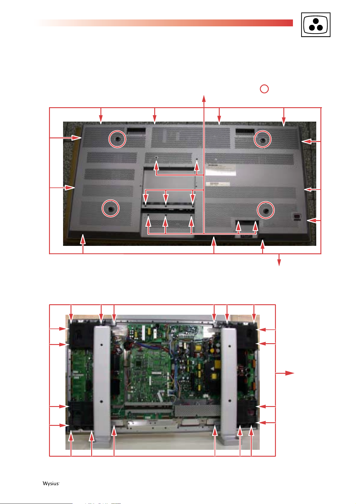
1. Removing the Leg Tube Assembly
Unscrew 4 screws from "Leg Tube Assembly." (Specification of screw driver is 15± 2kg), see fig.1
Push the "Leg Tube Assembly." downward to unlock and pull it away from unit, then unscrew 4 screws from rear cover.
(Specification of screw -driver is 15± 2 kg),
6 First issue 06 /03
Fig. 1
Fig. 2
HOW TO EXCHANGE THE MASK & PANEL PROCEDURE
Page 7
First issue 06 / 03 7
2. Removing the rear cover
Unscrew 12 screws from rear cover, see red arrow (Specification of screw driver is 15± 2 kg)
Unscrew 8 screws from rear cover, and unscrew 2 screws from AC power socket, see red arrow (Specification of screw driver
is 9± 1 kg)
Unscrew 4 screws from rear cover, see red circle (Specification of screw driver is 15± 2 kg)
3. Removing the screws from panel:
Unscrew 20 pieces of screw from panel site (Specification of screw driver is 15± 2 kg)
10 screws
12 screws
4 screws
Fig. 3
20 screws
Fig. 4
Page 8
8 First issue 06 /03
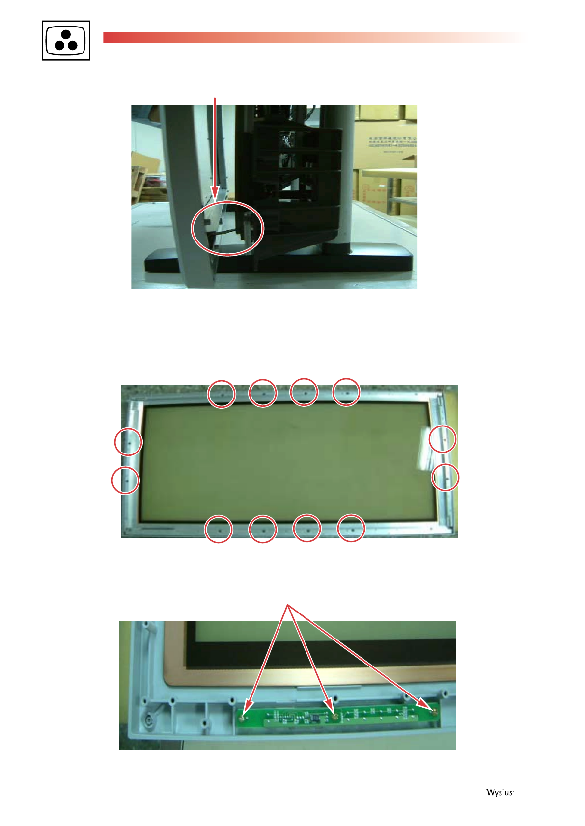
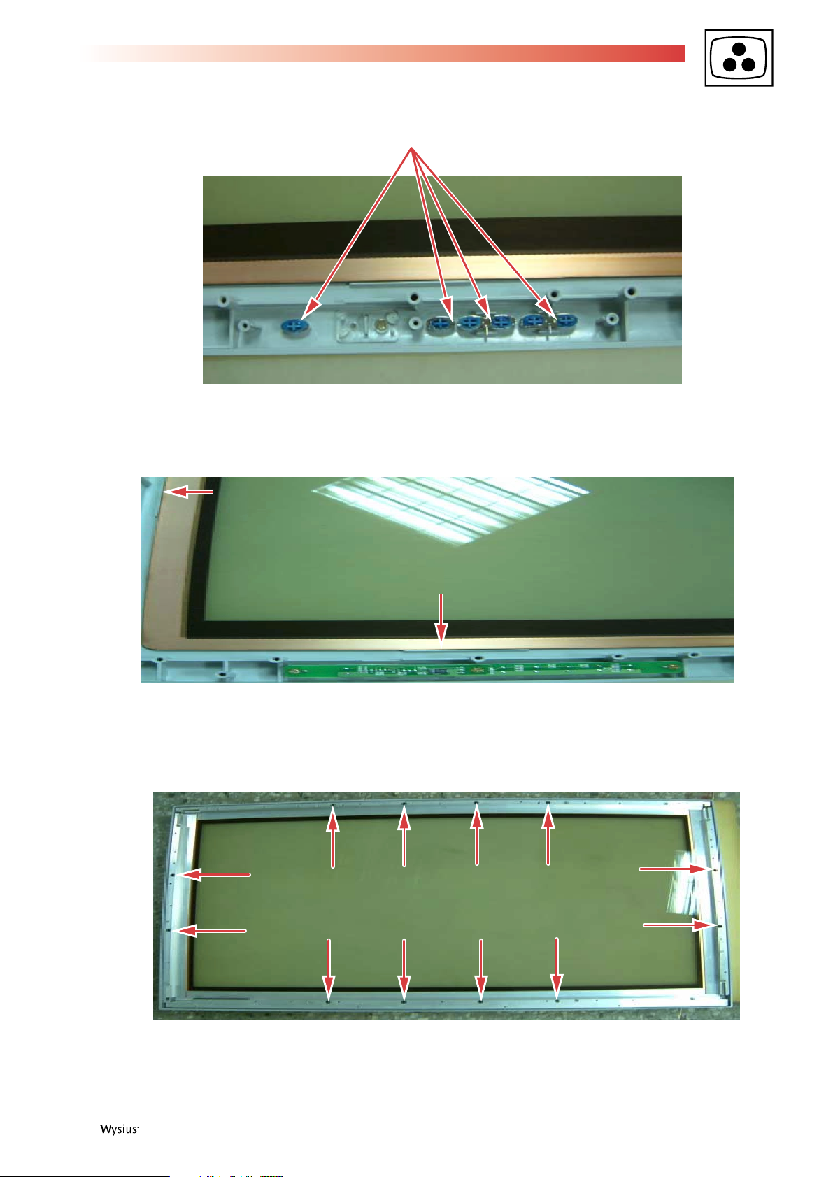
4. Removing the Mask and the J5 cable from PCB
5. Removing the filter
Unscrew 10 screws from mask (Specification of screw driver is 15± 2 kg), then remove four angles that hold the PDP filter. (Be
careful: Please do not bump or scrape when handling the PDP filter.)
Before putting panel back clean PDP filter make sure it's free from dust.
Unscrew 3 screws and remove control board
3 screws
Fig. 6
Fig. 7
J5
Fig. 5
Page 9
First issue 06 / 03 9
Remove the Control buttons from old Mask and reinstall them on the new Mask.
Please to aim at red arrow to guide and there is have a channel when you put down glass back to new mask
Assemble 4 irons back to mask. Be careful: When you lock up 4 irons that screws should be to lock up on "SL&G" point.
6. Proceed in reverse order to re-assemble
Control buttons
Fig. 8
Fig. 9
Top side
Top bottom
Fig. 10
Page 10
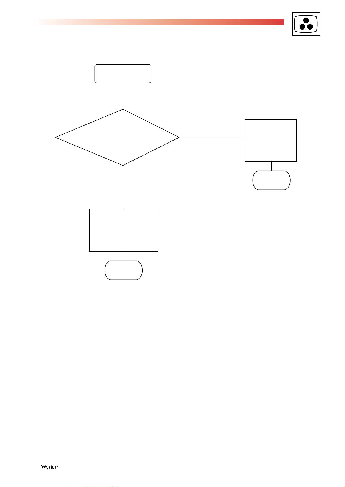
10 First issue 06 /03
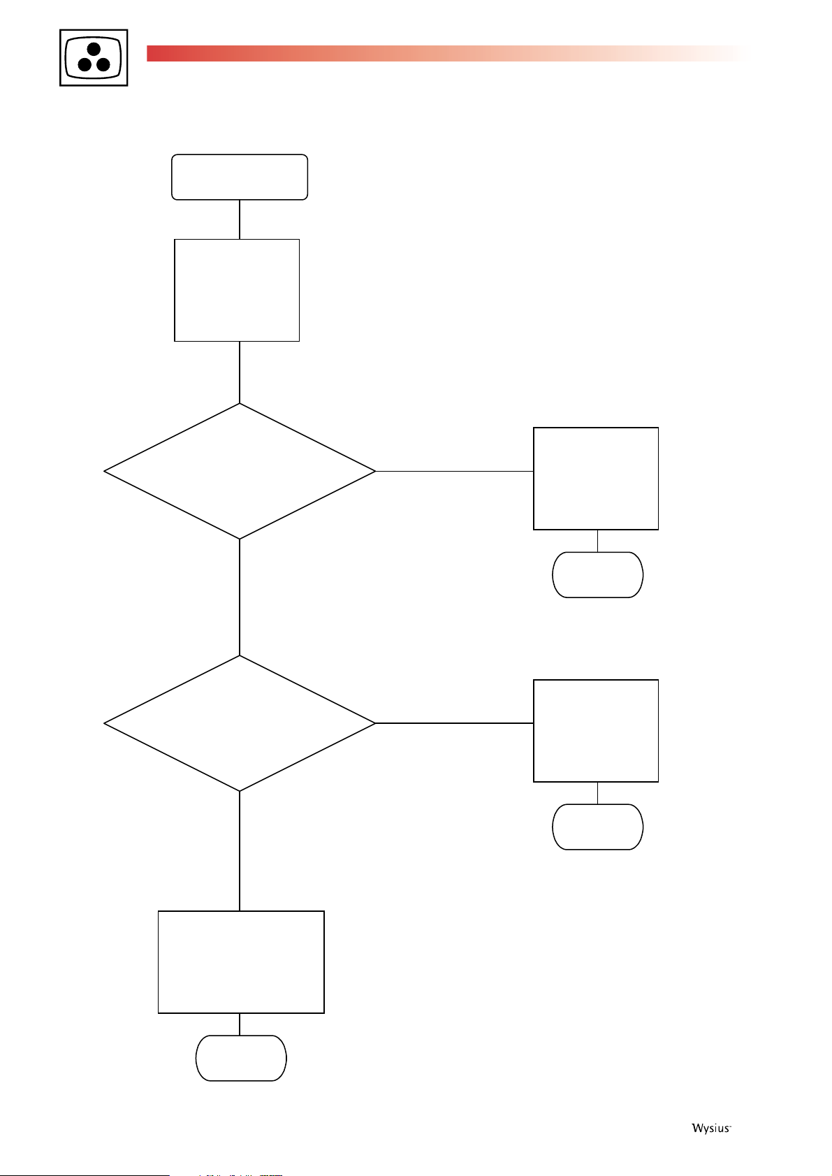
TROUBLESHOOTING
No power
Switch the
power on
Check "Power Imput" module
Check Panel Power Supply
Not correct
Correct
Not correct
Correct
Replace
"Power input"
module
Replace
Panel Power
Supply
Replace Standby
& Audio Power
Supply
End
End
End
Page 11
First issue 06 / 03 11
No picture
Check Image board
Not correct
Correct
Replace
Image board
Replace
PDP module
End
End
Page 12

12 First issue 06 /03
Vertical line fail
Check Interface Board-Z
Check X Amp Board-Left
Not correct
Correct
Not correct
Correct
Replace
Interface
Board-Z
Replace
X Amp
Board-Left
Replace
PDP module
End
End
Check X Amp Board-Right
Not correct
Correct
Replace
X Amp
Board-Right
End
End
Page 13

First issue 06 / 03 13
Horizontal line fail
Check Interface Board-Y
Check Y Amp Board-Top
Not correct
Correct
Not correct
Correct
Replace
Interface
Board-Y
Replace
Y Amp
Board-Top
Replace
PDP module
End
End
Check Y Amp Board-Bottom
Not correct
Correct
Replace Y Amp
Board-Bottom
End
End
Page 14

14 First issue 06 /03
No command
Switch the
power on
Check remote control
Check Front Button
Control Board
Not correct
Correct
Not correct
Correct
Replace the
battery or the
remote control
Replace
Front Button
Control Board
Replace Image
Board
End
End
End
Page 15

First issue 06 / 03 15
ADJUSTMENTS
PANEL voltage adjustment
Power voltage adjust for TTL panel
The power voltage should be adjusted and checked when changing the panel or power board
1. Setting input source to RGB mode.
2. RGB mode pattern is all white pattern.
3. Follow the panel label voltage to adjust VR (Va=75V, Vs=175V, -Vy=-80, Vset_up=220V)
4. Check voltage between ”check point” and ground.
5. Adjust sequence VA, VS, -Vy and Vset_up
Panel exchange the main power board adjust voltage for each Mode:
Digital Voltage meter the negative(-) to get main power board:(GND) PCB pin.
1. Digital Voltage meter the anode(+) to get main power board: (Va) CN805 or CN806 Va Connect pin.
Adjust VR (Va) = 75 ±0.3Vdc
2. Digital Voltage meter the anode(+) to get main power board: (Vs) CN803 or CN804 Vs Connect pin.
Adjust VR (Vs) = 175 ±0.3Vdc
MAIN POWER BOARD
*NOTE: ADJUSTMENT KNOB
V
Vs ADJ
-Vy ADJ
Vset ADJ
Va ADJ
GND POINT
Page 16

16 First issue 06 /03
Digital Voltage meter the negative(+) to get main power board:(GND) PCB pin.
3. Digital Voltage meter the anode(-) to get main power board: (-Vy) CN802 Vy Connect pin.
Adjust VR (-Vy) = -80 ±0.3Vdc
4. Digital Voltage meter the anode(-) to get main power board: (Vset_up) CN802 Vset_up Connect pin.
Adjust VR 105(Vset) = 220 ±0.3Vdc
5. All Voltage: DC(=) 5Vdc , 15Vdc
Color Temperature Adjustment
1.1 Color Temperature setting in DVI Mode
1. Turn on PDP set and warm up for over 30 minutes.
2. Turn on Color Analyzer CA-100 and reset CA-100.
3. Switch PDP input signal source to DVI mode.
4. Set up Video Pattern Generator (Astro, Model= VG-828H).
Timing set = 640 x 480 @ 60Hz;
Video = Panel Link (the DVI output mode)
Connect PDP DVI input connector with Astro to receive DVI signal.
Vs AD J VR102 Va AD J VR105 Vset AD J VR104
-
Vy AD J VR103
PS : Every mode voltage values are print on the label in each panel
Page 17

First issue 06 / 03 17
5. Dark level and bright level center block definition:
A. Dark level center block definition:
[WINDOW]
Mode %
Format 1 Window
Flicker None
Size H/V 28.5/34.0 (%)
Analog R/G/B 25/25/25 (10 IRE white output pattern)
B. Bright level center block definition:
[WINDOW]
Mode %
Format 1 Window
Flicker None
Size H/V 28.5/34.0 (%)
Analog R/G/B 153/153/153 (60 IRE white output pattern)
6. There are 2 different modes (DVI and RGB) color temperature setting; there are 3 different color temperatures (7180K,
8680K and 10180K) in each mode. Each color temperature needs to adjust dark level, bright level, and R, G, B.
The OSD menu for color temperature factory setting can be viewed by following the ”Factory Setting Procedure”.
Factory Setting Procedure:
A. Press (Zoom -) key for over 5 seconds and release.
B. Press (Zoom+) key for over 5 seconds and release.
C. Press ”ok” key.
D. Factory setting OSD menu shows up. The values shown up on the OSD menu are the factory default setting values.
The factory default setting values differ from each PDP panel module. The color temperature factory setting OSD menus
are as the following:
*Note: When adjusting the color temperature, please note
what is the input source and what input the PDP is, the input
source and the PDP input mode should be the same.
7. Put the color analyzer CA-100 in the center of the screen.
1.2 Adjusting procedure
1. Receive Astro VG-828H DVI dark level center block signal (10 IRE), follow the ”Factory Setting Procedure” to go into
factory setting mode and you will see the 7180K color temperature setting OSD menu.
2. 7180K dark level center block adjustment procedure:
A. Press (Zoom -) or (Zoom+) key in remote control to select G-BIAS, and adjust Y=0.35 FL±0.1FL
B. Press(Zoom -) or (Zoom+) key in remote control to select R-BIAS, and adjust x=308±15FL
C. Press (Zoom -) or (Zoom+) key in remote control to select B-BIAS, and adjust y=298±15FL
D. Adjust R/G/B-BIAS, make sure the final value x=308±15FL, y=298±15FL, Y=0.35FL±0.1FL
A. 7180K
DV I -CT : 718 0
K
[x : 3 0 8 y : 2 9 8]
GA IN B IAS
RG B RG B
xx xx xx xx xx xx
xx xx
B. 8680K
DV I -CT : 868 0
o
K
[x : 2 8 8 y : 3 0 1]
GA IN B IAS
RG B RG B
xx xx xx xx xx xx
xx xx
C. 10180K
DV I -CT :1018 0
o
K
[x : 2 7 0 y : 2 9 2]
GA IN B IAS
RG B RG B
xx xx xx xx xx xx
xx xx
Page 18

18 First issue 06 /03
3. 7180K bright level center block adjustment procedure:
(Please set Astro VG-828H DVI bright level center block signal to 60 IRE)
A. Press (Zoom -) or (Zoom+) key in remote control to select G-GAIN, and adjust Y=40±2FL
B. Press (Zoom -) or (Zoom+) key in remote control to select R-GAIN, and adjust x=308±15FL
C. Press (Zoom -) or (Zoom+) key in remote control to select B-GAIN, and adjust y=298±15F
D. Adjust R/G/B-GAIN, make sure the final value x=308±15FL, y=298±15FL, Y=40±2FL.
E. Press (Zoom+) key in remote control to select GAIN Gamma, and then press (Zoom -) or (Zoom+) key to adjust to Y=40
F. Press (Zoom+) key in remote control to select BIAS Gamma, and then press (Zoom -) or (Zoom+) key to adjust to Y=0.35
4. When you want to go ahead for next color temperature setting, double check the Gamma values, make sure GAIN
Gamma and BIAS Gamma values are correct, and then press the ”ok” key in remote control. For each color temperature
setting, please repeat the procedure (1)-(3). Only x and y value will change in different color temperature mode (in 8680K,
x=288, y=301; in 10180K, x=270, y=292) and Y values are all the same in each color temperature mode (dark level Y=0.35,
bright level Y=40).
2.1 Color Temperature setting in RGB Mode
1. Turn on Color Analyzer CA-100 and reset CA-100.
2. Switch PDP input signal source to RGB mode.
3. Set up Video Pattern Generator (Astro, Model= VG-828H).
Timing set = 640 x 480 @ 60Hz;
Video = Analog (the RGB output mode)
Connect PDP RGB input connector with Astro to receive RGB signal.
4. Dark level and bright level center block definition:
A. Dark level center block definition:
[WINDOW]
Mode %
Format 1 Window
Flicker None
Size H/V 28.5/34.0 (%)
Analog R/G/B 25/25/25 (10 IRE white output pattern)
B. Bright level center block definition:
[WINDOW]
Mode %
Format 1 Window
Flicker None
Size H/V 28.5/34.0 (%)
Analog R/G/B 153/153/153 (60 IRE white output pattern)
5. There are 2 different modes (DVI and RGB) need color temperature setting; there are 3 different color temperatures
(7180K, 8680K and 10180K) in each mode. Each color temperature needs to adjust dark level, bright level, and R, G, B.
The OSD menu for color temperature factory setting can be viewed by following the ”Factory Setting Procedure”.
Factory Setting Procedure:
A. Press (Zoom -) key for over 5 seconds and release.
B. Press (Zoom+) key for over 5 seconds and release.
C. Press ”ok” key.
D. Factory setting OSD menu shows up.
The values showed up on the OSD menu are the factory default setting values. The factory default setting values differ from
each PDP panel module. The color temperature factory setting OSD menus are as the following:
Page 19

First issue 06 / 03 19
*Note: GAIN Gamma and BIAS Gamma have no
function under RGB mode.
*Note: When adjusting the color temperature,
please note what is the input source and what input
the PDP is, the input source and the PDP input
mode should be the same.
6. Put the color analyzer CA-100 in the center of the screen.
2.2 Adjusting procedure:
1. Receive Astro VG-828H RGB dark level center block signal (10 IRE), follow the ”Factory Setting Procedure” to go into
factory setting mode and you will see the 7180K color temperature setting OSD menu.
2. 7180K dark level center block adjustment procedure:
A. Press (Zoom -) or (Zoom+) key in remote control to select G-BIAS, and adjust Y=0.35 FL±0.1FL
B. Press (Zoom -) or (Zoom+) key in remote control to select R-BIAS, and adjust x=308±15FL
C. Press (Zoom -) or (Zoom+) key in remote control to select B-BIAS, and adjust y=298±15FL
D. Adjust R/G/B-BIAS, make sure the final value x=308±15FL, y=298±15FL, Y=0.35FL±0.1FL
3. 7180K bright level center block adjustment procedure:
(Please set Astro VG-828H RGB bright level center block signal to 60 IRE)
A. Press (Zoom -) or (Zoom+) key in remote control to select G-GAIN, and adjust Y=40±2FL
B. Press (Zoom -) or (Zoom+) key in remote control to select R-GAIN, and adjust x=308±15FL
C. Press (Zoom -) or (Zoom+) key in remote control to select B-GAIN, and adjust y=298±15F
D. Adjust R/G/B-GAIN, make sure the final value x=308±15FL, y=298±15FL, Y=40±2FL.
4. When you want to go ahead for next color temperature setting, double check the Gamma values, make sure GAIN Gamma
and BIAS Gamma values are correct, and then press the ”ok” key in remote control. For each color temperature setting,
please repeat the procedure (1)-(3). Only x and y value will change in different color temperature mode (in 8680K, x=288,
y=301; in 10180K, x=270, y=292) and Y values are all the same in each color temperature mode (dark level Y=0.35, bright
level Y=40).
A. 7180K
RGB -CT : 7 1 8 0
o
K
[x :308 y :298]
GA IN B IAS
RG B RG B
xx xx Xx xx xx xx
xx xx
B. 8680K
RGB -CT : 8 6 8 0
o
K
[x :288 y :301]
RGB -CT: 1
[x : 2 7 0 y :
GA IN B IAS
RG B R
GA IN B
RG B R
GB
Xx xx Xx xx xx xx
xx xx
C. 10180K
0180
o
K
:292]
IAS
GB
xx xx xx x xx xx
xx xx
(GAIN Gamma) (BIAS Gamma)
Page 20

20 First issue 06 /03
BLOCK DIAGRAMS
Panel Pow er
Supply
Module
Speaker
PANEL (X -D RV)
Speaker
Fr ont B utton
Contro l
Board
PD P P ANEL MO DUL E
Logic
Bo ard
VG A IN
DVI IN
RS232 IN
Audio
Am p lifier
Board
Interfa ce
Board-Z
X A m p
Board-Right
AC M a ster
Power Sw itch
Board
X A m p
Board-Left
Po w e r Input
Module
AC IN
Y A m p
Board-Top
Im age
Bo ard
PANEL (Z -DRV)
Y A m p
Board-Botto m
S ta ndb y &
Au d io P o w e r
Supply Board
Interface
Board-Y
PANEL (Y-D RV)
Page 21

First issue 06 / 03 21
SCHEMATIC DIAGRAMS
SUB-WOOFER
SU B_WFR
IC S 1
NJM455 8M
1
2
3
4 5
6
7
8
Rc h
+
CS 2
10uF
16V
RS 1
22K
1/16W
+CS1
47uF
16V
GN D
5V
12V_0
RS 7
10K
1/16W
1/2VC C
IC S 2
TC 4W53F U
1
2
3
4
8
7
6
5
CO M
IN H
VEE
VSS
VD D
CH0
CH1
AD R
Lch
RS 5
47K
1/16W
SU B_WFR
MUTE_1
SUB_WOOFER O UT
SMD
CS 4
0.1uF
16V
CS 5
0.047 uF
16V
5V
GN D
12V_0
RS 6
10K
1/16W
RS 4
47K
1/16W
RS 2
22K
1/16W
Lch
Rc h
RS 3
47K
1/16W
MUTE_1
1/2VC C
+
CS 3
10uF
16V
Page 22

22 First issue 06 /03
VIDEO SYSTEM REGULATOR POWER
D
C 325
0.1uF
25V
Z
D
C 317
0.1uF
25V
Z
C3 20
0.01uF
50V
D
D
For IP00C711
D
D
C 319
0.1uF
25V
Z
D
D
V33T MP
+
C 323
100uF
16V
C3 32
0.01uF
50V
C 314
0.01uF
50V
D
C 327
0.1uF
25V
Z
+
C 309
100uF
16V
D
DD
D
+
C 321
100uF
16V
D
D
C 316
0.01uF
50V
P5V
U6 2
BA033
1
2
3
VIN
GN D
VOU T
D
D
D
U6 0
BA033
1
2
3
VIN
GN D
VOU T
C 330
0.01uF
50V
D
C 326
0.01uF
50V
+
C 312
10uF
16V
+
C 324
10uF
16V
C 315
0.1uF
25V
Z
D
V33SB
D
U6 3
BA033
1
2
3
VIN
GN D
VOU T
+
C 311
100uF
16V
V33
D D
D
C 318
0.01uF
50V
D
C 329
0.1uF
25V
Z
P5V
SB5V
P5V V33P
+
C 322
10uF
16V
D
C 331
0.1uF
25V
Z
+
C 310
10uF
16V
C 313
0.1uF
25V
Z
D
C 328
0.01uF
50V
U6 1
BA033
1
2
3
VIN
GN D
VOU T
D
Page 23

First issue 06 / 03 23
DIGITAL SYSTEM (CPU - EEPROM - I/O)
SO P[5]
POWER_ON
P4
P2
A6
RGBn_DVI
L2
0
1/8W
R51
N/820
1/16W
INT _DPT V_S
YUVn_RGB P[9]
P6
A15
A4
AFT_T UN
C5
0.1uF
25V
Z
R395
N/10
1/16W
T
C6
10PF
50V
D
SOGn P[9]
R8 47 1/16W
D1
RLS4148
D
WRn_DP T V
A18
R7 3.3K 1/16W
SB5V_IO
A0
R20 33 1/16W
SB5V_CPU
D
D
V2B_DETn P[18]
A14
R13
47
1/16W
D
SURR2 P[18]
SB_LED
J2
N/CON3
1
2
3
V
I
N
V
O
U
TGND
U5
S80845ANUP
12
3
SB5V_CPU
OCKINV P[8]
P4
P6
P1
P3
A2
Q2
2SC2412KBQ
R27
22K
1/16W
PLLDAT A P[3]
REST Q
A2
A17
TMS
A8
R36 10K 1/16W
R28
4.7K
1/16W
R14
N/3.3K
1/16W
SB5V
TXDP[2]
A10
R342
0
1/16W
U4
HD641 307 9F
22
23
24
25
26
27
28
29
31
32
33
34
35
36
37
38
39
40
13141516171819
20
45
44
51
52
46
47
48
57
49
54
55
56
69
70
71
72
9
10
11
43
41
42
73
74
75
76
77
78
79
80
1
2
3
4
5
6
7
8
59
60
61
62
63
64
65
66
21
68
53
12
58
50
30
67
A0
A1
A2
A3
A4
A5
A6
A7
A8
A9
A10
A11
A12
A13
A14
A15
A16
A17
D0D1D2D3D4D5D6
D7
MD1
MD0
EXTAL
XTAL
@
STB Y
RES
RESO
NMI
AS
RD
WR
P80/IRQ0
P81/IRQ1
P82/IRQ2
P83/IRQ3
P90/TXD
P92/RXD
P94/SCK/IRQ4
P60/WAIT
A18
A19
PA0/TCLKA
PA1/TCLKB
PA2/TIOCA0/TCLKC
PA3/TIOCB0/TCLKD
PA4/TIOCA1/A23
PA5/TIOCB1/A22
PA6/TIOCA2/A21
PA7/TIOCB2/A20
PB0/TIOCA3
PB1/TIOCB3
PB2/TIOCA4
PB3/TIOCB4
PB4/T OCXA4
PB5/T OCXB4
PB6
PB7/ADTRG
P70/AN0
P71/AN1
P72/AN2
P73/AN3
P74/AN4
P75/AN5
P76/AN6
P77/AN7
VCC
AVCC
VCC
VSS
AVSS
VSS
VSS
VREF
R37 10K 1/16W
R30
22K
1/16W
D
D
F4
0
1/8W
AVB_DETn
TE LETEXT_ON P[19]
GND
SB5V_M
RXDP[2]
SCS
LD002
N/LED
+
C428
4.7uF
35V
C11
0.1uF
25V
Z
A6
R411
10K
1/16W
R71
N/0
1/16W
INT_USB
R41 N/0 1/16W
SB5V_CPU
SDA2
INT_RT C
INT_DPT V
REMOT E
P5
EEPROM(DIP32)
INT_USB
SDA0
R24 33 1/16W
T
C18
120PF
50V
D
INT_RT CP[2]
A11
A5
D
AC_DE T P[18]
P1
A11
U68
AM C7630-5
1
2
3
4 5
6
7
8
VIN
GND
GND
EN GND
GND
GND
VOUT
R31 33 1/16W
D
SCLK
D_CTL
SB5V_CPU
PLLCLK P[3]
R34
22K
1/16W
PLLDAT A
TP7
SCL1
T
C17
120PF
50V
D
D
GIVS P[7]
HSYNC_SP
A18
SB5V_M
TMS
TC K
A14
SB5V_IO
RSTnC711 P[5,8]
RC_IN
A10
A7
U6A
74LVT04
1 2
14
7
A0
A9
R15
3.3K
1/16W
RP5
10K ohm
1 8
2 7
3 6
4 5
TUN_DETn
SCART_CTL1
SCL1
SCL2
V2B_DETn
SDA2 P[2,4,7,18]
HSYNC_SP
A13
R11
N/47
1/16W
U8
EM83010
18
10
11
12
13
14
15
16
17
9
1
2
8
7
6
5
4
3
VDD
P10
P11
P12
P13
P14
P15
P16
P17
VSS
SDT
SCK
P05
P04
P03
P02
P01
P00
R10 33 1/16W
RP3
10K ohm
18
27
36
45
SB5V
ST ANDBY
U6E
74LVT04
11 10
14
7
T
C3
33PF
50V
SCL0
P3
A15
A19
R26
10K
1/16W
R46
N/560K
1/16W
SPK_CTL P[18]
A3
A7
R50
N/820
1/16W
+
C10
10uF
16V
U1
A5-32-10VC 4
1
2
3
8
2512
16
38
6
17
9
10
11
13
14
5
27
28
39
4726
29
15
18
19
20
21
22
23
24
30
31
32
33
34
35
36
37
40
41
42
43
44
I/O5
I/O6
I/O7
I/O8
I/O23I/O12
VCC
VCC
GND
GND
I/O9
I/O10
I/O11
I/O13
I/O14
CLK0
CLK1
GND
GND
TD1
TC K
TMS
TDO
I/O15
I/O16
I/O17
I/O18
I/O19
I/O20
I/O21
I/O22
I/O24
I/O25
I/O26
I/O27
I/O28
I/O29
I/O30
I/O31
I/O0
I/O01
I/O02
I/O03
I/O04
R2
N/1.5K
1/16W
T
C19
120PF
50V
SB5V_M
P7
A1
A3
ST ANDBY
U7 Socket
I1177-108-1
2
3
4 5
6
7
8
+C13
10uF
16V
RP2
10K ohm
1 8
2 7
3 6
4 5
TDO
P0
A16
R9
47
1/16W
SB5V
D
RDn_DPT V
SCART_CTL1
SDA0
NMI
PLLCLK
A9
R22
10
1/16W
R70
N/0
1/16W
D
SB5V
+C9
10uF
16V
JP1
N/HEADER 3X2
12
34
56
SB5V_CPU
SB5V_CPU
R45
N/560K
1/16W
SB5V_CPU
SB5V_CPU
RP1
10K ohm
1 8
2 7
3 6
4 5
SCL2
C1
0.1uF
25V
Z
D
SCL0
D
P0
U6B
74LVT04
3 4
14
7
SB5V_CPU
CPU5V
TDI
A16
A1
A17
C25
0.1uF
25V
Z
R413
N/0
1/16W
TP8
SB5V
D
P5
LD001
N/LED
D
F3
0
1/8W
R6
100K
1/16W
R23
10
1/16W
GIHS
TDO
R396
N/10
1/16W
R33 33 1/16W
TP13
HSYNC_MP
R412
10K
1/16W
R12 33 1/16W
T
C7
10PF
50V
D
SI P[5]
A15
TC K
A7
SO
C23
0.1uF
25V
Z
SO1
N/W27C010_5
22
24
13
14
15
17
18
19
20
21
31
32
1
16
12
11
10
9
8
7
6
5
27
26
23
25
4
28
29
3
2
30
CE
OE
Q0
O1
O2
O3
O4
O5
O6
O7
PGM
VCC
VPP
GND
A0
A1
A2
A3
A4
A5
A6
A7
A8
A9
A10
A11
A12
A13
A14
A15
A16
A17
TP4
P5V
SCART_RGB
A13
D
CPU5V
U7
M24C16WBN6
1
2
3
45
6
7
8
A0
A1
A2
VSSSDA
SCL
TEST
VCC
PLLCLK
A14
R21 33 1/16W
SCART_CTL2
TUN_DETn
A12
A16
R25
5.6K
1/16W
R344
0
1/16W
R40
10
1/16W
R17
3.3K
1/16W
RESET
J5
CP0316-EJST -
1
2
3
4
5
6
D
SB5V_CPU
Q4
2SC2412KBQ
SB5V
A0
SDA1
SOGn
P4
A1
SW_IN
RT15
N/0
1/16W
R5
10K
1/16W
D
A[0..19]
R39 10K 1/16W
L3
0
1/8W
R399
N/0
1/16W
ON_LED
SB5V
D
A2
SI
SDA0
NEC_PSO
A17
T
C16
120PF
50V
R18 33 1/16W
SB5V_IO
P7
A0
A11
RP8
10K ohm
1 8
2 7
3 6
4 5
D
PS_DPT V
P[0..7]
PLLDAT A
P0
AVB_DETn
P6
A4
R32
4.7K
1/16W
D
15Kn_MP
L1
N/0
1/8W
R44
N/560K
1/16W
P1
P7
SB5V_IO
F1
0
1/8W
MPU
SB5V
NEC_PSM
A12
C8
0.1uF
25V
Z
D
A3
R52
N/820
1/16W
J4
N/CON3
1
2
3
SCS P[5]
P2
Q1
2SC2412KBQ
R3
N/1.5K
1/16W
TP16
YUV_SPSW P[18]
A19
U6C
74LVT04
5 6
14
7
D
D
A4
A1
U6D
74LVT04
9 8
14
7
R343
N/0
1/16W
R4 N/0 1/16W
R16
3.3K
1/16W
SB5V
CEn
T
C375
120PF
50V
+
C15
10uF
16V
PNL_CTLn P[4]
TDI
REMOT E
ALE_DPT V
INT_DPT V
D
AFT_T UN
GIVS
A12
SB5V_M
D
P3
+C42.2uF
50V
T
C2
33PF
50V
R29
5.6K
1/16W
SB5V_CPU
POWER_ON
SB5V_CPU
TP5
PD_DVIn P[8]
HSYNC_MP
A6
R345
0
1/16W
R19 33 1/16W
+
C426
1uF
50V
SCART_CTL3
KEY PAD_IN
A5
A10
D D
GIHS P[7]
RGBn_DVI P[3,18]
P[0..7]
A8
A9
U3
29C 020C P90BS
12
11
10
9
8
7
6
5
27
26
23
25
4
28
29
3
2
22
24
13
14
15
17
18
19
20
21
32
1
31
16
30
A0
A1
A2
A3
A4
A5
A6
A7
A8
A9
A10
A11
A12
A13
A14
A15
A16
CE
OE
D0
D1
D2
D3
D4
D5
D6
D7
VCC
VPP
PGM
GND
A17
NEC_BLK P[4]
U6F
74LVT04
13 12
14
7
KEY PAD_IN
YUV_SW P[18]
MODE P[4]
D
P5
R349
N/1M
1/16W
R394
N/10
1/16W
D
SCLK P[5]
INT _DPT V_S
P0
A8
Y1
16MHz
SB5V_CPU
TP14
D
P2
A2
FREEZE P[5]
A_MUTEn P[18]
SDA1
A17
PD_9884n P[7]
SDA2
SB P[18]
F2
0
1/8W
T
C20
120PF
50V
S_DET
AO_SEL P[18]
A13
C12
0.1uF
25V
Z
R1
10K
1/16W
R35
22K
1/16W
SURR1 P[18]
PGMn
RP
9
10K ohm
182736
45
RST_DPTV
NMI
+
C14
10uF
16V
Q3
2SC2412KBQ
U3 Socket
I1514-132-S
1
2
3
4
5
6
7
8
9
10
12
11
14
13
16
15
30
29
28
27
26
25
24
23
22
21
20
19
18
17
31
32
J3
N/CON4
1
2
3
4
VS_POL
HS_POL
SB5V
D
SCL2 P[2,4,7,18]
A5
R38
10
1/16W
SCL0
A3
C24
0.1uF
25V
Z
Page 24

24 First issue 06 / 03
DIGITAL SYSTEM (OSD - USB - RS232)
D
R316
N/220
1/16W
D
T
C416
N/22PF
50V
SC L2_33
T
C35
180PF
50V
R62
0
1/16W
B_O SD P[5]
TP 25
D
5V_O SD
SD A2_33
R69A 33 1/16W
D
INT_RTCP[1]
C42
N/0.1u F
25V
Z
SC L2_33P[7]
V33
P1
D1553- 109- 5
9
4
8
3
7
2
6
1
10
11
R69 N /33 1/16W
Q6
BSN 20
2
1
3
U12
HIN 232C B
16
15
11
12
13
14
7
8
9
10
1
3
4
5
2
6
VC C
GN D
T1 -I N
R1-O UT
R1-IN
T1 -O U T
T2 -O U T
R2-IN
R2-O UT
T2 -I N
C1+
C1C2+
C2-
V+
V-
D52
N/R LS4148
D
TP 21
RP12
10K ohm
1 8
2 7
3 6
4 5
R60
47
1/16W
M8p
Q5
BSN 20
2
1
3
R55
N/1K
1/16W
SC L2
RXD P [1]
BSN20
+
C32
N/10uF
16V
D
SD A2
R56
N/1K
1/16W
T
C30
100PF
50V
D53
N/R LS4148
P5V
T
C26
N/12PF
50V
D
Y4
N/32.768KH Z
C21
N/0.1u F
25V
Z
SB5V
D(2)
SD A2_33P[7]
USB5V
+
C31
1uF
50V
R315
N/4.7K
1/16W
TP 22
R314
N/0
1/16W
V33
RXD
L4
0
1/8W
S(3)
R68A 33 1/16W
R61
47
1/16W
R66
100
1/16W
D
D
DTEN P [5]
L6
0
1/8W
D
D
R57
N/1K
1/16W
G(1)
U11
MTV13 0
8
7
6
5
4
3
2
1
9
10
11
12
13
14
15
16
SC K
SD A
SSB
HF LB
VD D
NC
XI N
VSS
VD D
VF LB
INT
FBKG
B-OU T
G-OUT
R-O U T
VSS
SC L2P[1,4,7,18]
VSY N C O P [4,5]
SC L2_33
SD A2P[1,4,7,18]
SD
SB5V
CTS
R64
N/220
1/16W
R68 N /33 1/16W
IIC ADDR:A2 H(W),A3 H(W)
SD A2
TP 23
D
DSR
T
C22
12PF
50V
V33SB
R_OS D P[5]
TXD P[1]
TXD
PO C LKO SDP[3]
D51
N/R LS4148
SC L2
R54
22
1/16W
R313
N/10K
1/16W
C28
0.1uF
25V
Z
R63
47
1/16W
5V_O SD
R67
100
1/16W
U65
N/PC F8563T
8
7
6
54
3
2
1
VC C
CLKO
SC L
SD AVSS
INT
OS C O
OS C I
+
C43
N/10uF
16V
D
RD
V33
INTENS ITY
DTR
+
C34
1uF
50V
R58
1K
1/16W
SB5V
D
+
C41
N/10uF
16V
P5V
C39
0.1uF
25V
Z
SB5V
L7
N/0
1/8W
RTC
TP 24
D
+
C27
10uF
16V
D
5V_O SD
HSYNCOP[4,5]
C33
0.1uF
25V
Z
T
C29
N/100PF
50V
D
+
C37
47uF
16V
C40
0.1uF
25V
Z
D
R59
47
1/16W
D
R65
100
1/16W
T
C36
180PF
50V
G_ OS D P[5]
C38
0.1uF
25V
Z
D
SD A2_33
RTS
C44
N/0.1u F
25V
Z
SB5V
Page 25

First issue 06 / 03 25
DIGITAL SYSTEM (HSYNC SW - CLOCK)
DVI_HSP[8]
R350
N/1 M
1/16W
T
C 404
22PF
50V
R7 7
33
1/16W
PIC LK P[5]
D
FROM CP U
0
DVI_PICKP[5]
Y
V33SB
TP 28
A/B
D
R8 0
33
1/16W
V33
R386
150
1/16W
C50
0.1uF
25V
Z
1
R8 2
4.7
1/16W
VCCP LL
T
C54
33PF
50V
D
RGBn_D VIP[1,18]
CLK
D
D
T
C51
12PF
50V
D
PIVS P[5]
Y3
14.318MHz
C49
N
+
C55
47uF
16V
FG V SP[7,8,9]
D
DVI-H, V,CLK
FG HS
PIHS P[5]
U1 5
74LVC 157
2
3
5
6
11
10
14
13
1
15
4
7
9
12
16
8
1A
1B
2A
2B
3A
3B
4A
4B
A/B
G
1Y
2Y
3Y
4Y
VC C
GN D
FG V S
R8 1
33
1/16W
U1 6
IC S9161A
13
3
6
7
5
1
2
4
8
9
10
11
12
14
15
16
VD D
AVD D
X1
X2
GN D
SEL0_C LK
SEL1_D AT A
OE
MC LK
VC LK
E RRO UT
EXTC LK
INIT 0
INIT 1
EXTSEL
PD
POC LKOSD P[2]
D
D
PLLC LKP[1]
POC LK
L13
0
1/8W
T
C53
N/47PF
50V
R7 8
33
1/16W
R8 3
33
1/16W
PLLH SOP[7]
VCCP LL
D
FG HSP[7,9]
T
C52
12PF
50V
D
R7 9
33
1/16W
CLK P[5,6]
DDCV SY NC P [7]
DATACKP[7]
PIHSS P[7]
PLLD AT AP[1]
D
DVI_VSP[8]
C57
0.1uF
25V
Z
C56
0.1uF
25V
Z
POCLK P [4,5]
RGB-H, V,CLK
Page 26

26 First issue 06 / 03
DIGITAL SYSTEM (BUFFER - PANEL CONNECTOR)
TP0
SC L2 P[1, 2,7,18]
BRGO UT 2
BRBOUT6
LG DISPEN
BOU T 1
BBO UT4
BHSYNCO
BRGO UT 4
C3 97
N/ 0. 1uF
25 V
Z
T
C3 68
47 PF
50 V
DS BLKH
BRGO UT 0
LG DISPEN
R73
N/ 0
1/16 W
BRROUT7
VC CBF
BGO UT 2
BBO UT5
D
SDA2
RO UT3
BBO UT2
BRROUT1
POC LKP[ 3,5]
POC LK
BRGO UT 5
T
C3 59
47 PF
50 V
BRGO UT 5
RP 36
22 o hm
1 8
2 7
3 6
4 5
JP 2
N/ HE AD E R 1X2
1 2
BVS YNCO
GOU T 4
BRROUT3
AGND3
TP0
GOU T 7
BRGO UT 3
PC LK_LG
U21
74LV C 244ADB
2
4
6
8
11
13
15
17
1
19
18
16
14
12
9
7
5
3
20
10
1A 1
1A 2
1A 3
1A 4
2A 1
2A 2
2A 3
2A 4
1G
2G
1Y 1
1Y 2
1Y 3
1Y 4
2Y 1
2Y 2
2Y 3
2Y 4
VC C
GN D
R3 46
N/ 0
1/16 W
P5V
BOUT [0..7]P[ 5]
RXI N3 -
BRROUT1
BRROUT0
RXCLKIN+
R84
N/ 0
1/16 W
T
C3 57
47 PF
50 V
HQ E N
RO UT6
BGO UT 4
BRGO UT 3
R3 90
N/ 0
1/16 W
RP 39
22 o hm
1 8
2 7
3 6
4 5
BOU T 6
C62
0.1 uF
25 V
Z
L14 ON
TP0
BGO UT 1
T
C3 65
47 PF
50 V
SD2
J20
CP1626-141-1
2
3
4
5
6
7
8
9
10
11
12
13
14
15
16
17
18
19
20
21
22
23
24
25
26
27
28
29
30
31
32
33
34
35
36
37
38
39
40
41
GN D
R0
R1
R2
R3
GN D
R4
R5
R6
R7
GN D
G0
G1
G2
G3
GN D
G4
G5
G6
G7
GN D
B0
B1
B2
B3
GN D
B4
B5
B6
B7
GN D
Hs ync
GN D
Vs ync
GN D
BLA NK
GN D
DCL K
GN D
DI SP EN
GN D
BRBOUT7
C3 95
N/ 0. 1uF
25 V
Z
R4 08
N/ 0
1/16 W
BRBOUT2
BRGO UT 7
R3 92
N/ 0
1/16 W
ROUT [0..7]P[ 5]
BROUT 2
BRBOUT2
U18
74LV C 244ADB
2
4
6
8
11
13
15
17
1
19
18
16
14
12
9
7
5
3
20
10
1A 1
1A 2
1A 3
1A 4
2A 1
2A 2
2A 3
2A 4
1G
2G
1Y 1
1Y 2
1Y 3
1Y 4
2Y 1
2Y 2
2Y 3
2Y 4
VC C
GN D
GOU T 1
BVS Y NCO
BRGO UT 1
BRGO UT 6
T
C3 61
47 PF
50 V
BBO UT0
BRROUT0
BRGO UT 7
L50 OF F
D
BBO UT1
BRBOUT4
RP 35
22 o hm
1 8
2 7
3 6
4 5
SC L2
BOU T 3
BGO UT 5
DISPEN
BLANKn
J19
N/ F H12-40S
1
3
5
7
9
11
13
15
17
19
21
23
25
27
29
31
33
35
37
39
2
4
6
8
10
12
14
16
18
20
22
24
26
28
30
32
34
36
38
40
BRBOUT3
T
C3 70
47 PF
50 V
U20
74LV C 244ADB
2
4
6
8
11
13
15
17
1
19
18
16
14
12
9
7
5
3
20
10
1A 1
1A 2
1A 3
1A 4
2A 1
2A 2
2A 3
2A 4
1G
2G
1Y 1
1Y 2
1Y 3
1Y 4
2Y 1
2Y 2
2Y 3
2Y 4
VC C
GN D
BBLANKn
RXIN1 +
T
C3 58
47 PF
50 V
+
C4 01
N/ 10uF
16 V
BROUT 0
VSY NCO
L17 OF F
DS BLKH
BRBOUT5
T
C3 56
47 PF
50 V
TP0
BRROUT3
BRBOUT0
BRROUT1
BROUT 7
PC LK_LG
T
C3 67
47 PF
50 V
P5V
BGO UT 6
BROUT 0
L14 OF F
SC 2
+
C4 00
N/ 10uF
16 V
BROUT 3
C61
0.1 uF
25 V
Z
TTL
RXI N0 -
D
TP0
BRBOUT7
DS HS Y NCO
GOU T 5
DS HS Y NC0
U66
N/ DS 90C F 383A
1
9
17
26
44
34
31
50
2
51
52
54
55
56
3
8
10
4
6
7
11
12
14
5
13
21
29
33
30252728321618151920222324
35
36
43
49
53
40
39
48
47
46
45
42
41
38
37
VC C
VC C
VC C
VC C
LVD S VC C
PLL VCC
TxCLK IN
TxIN27
TxIN5
TxIN0
TxIN1
TxIN2
TxIN3
TxIN4
TxIN6
TxIN10
TxIN11
TXIN7
TxIN8
TxIN9
TxIN12
TxIN13
TxIN14
GN D
GN D
GN D
GN D
PLL GN D
TxIN26
TxIN23
TxIN24
TxIN25
PWR D WN
TxIN16
TxIN17
TxIN15
TxIN18
TxIN19
TxIN20
TxIN21
TxIN22
PLL GN D
LV D S G N D
LV D S G N D
LV D S G N D
GN D
TxCLKOUT -
TxCLKOUT+
TxOUT0TxOUT0+
TxOUT1TxOUT1+
TxOUT2TxOUT2+
TxOUT3TxOUT3+
RP 42
N/ 0
1 8
2 7
3 6
4 5
D
BROUT 4
BPC LKO
TP0
BRROUT7
BRBOUT6
T
C3 71
47 PF
50 V
L50 ON
R3 47
N/ 0
1/16 W
BBO UT3
R1 31
N/ 0
1/16 W
T
C3 55
47 PF
50 V
BBO UT4
BRROUT5
BRROUT6
BROUT 6
GOU T 3
RO UT1
L17
N
R1 30
N/ 0
1/16 W
POC LK
HS Y NCO
PNL_CT Ln
VC CBF
MO DE
RXIN3 +
RXI N2 -
C63
0.1 uF
25 V
Z
L17 ON
BROUT 3
NE C _BLK
+
C3 99
N/ 10uF
16 V
J18
N/ F H12-40S
1
3
5
7
9
11
13
15
17
19
21
23
25
27
29
31
33
35
37
39
2
4
6
8
10
12
14
16
18
20
22
24
26
28
30
32
34
36
38
40
RXI N1 -
BRGO UT 6
R86 22 1/16 W
VC CBF
T
C3 72
47 PF
50 V
BBL ANKN
BRROUT3
D
LVD S33
BROUT 6
RXIN0 +
DS VSY NCO
R3 48 N/ 22 1/ 16W
R3 91
N/ 0
1/16 W
D
BGO UT 7
GOU T [0..7 ]
BROUT 4
BGO UT 3
BBO UT6
BRGO UT 2
C3 98
N/ 0. 1uF
25 V
Z
TP0
BOUT [0..7]
+C59
N/ 47uF
16 V
BLANKnP[ 5]
BGO UT 0
GOU T 6
PNLCT L33
BRBOUT3
BRROUT5
BRROUT2
BGO UT 4
BRBOUT4
RO UT5
BRGO UT 0
R4 02
N/ 0
1/16 W
BGO UT 5
BRGO UT 0
DCL K
L14
0
1/8W
DS CLKI N
BRROUT4
BRROUT6
DS VSY NC0
L50
N/ 0
1/8W
BBO UT0
BROUT 5
DS HS Y NC0
BPC LKO
RO UT2
BBO UT1
LVD S33
NE C _BLKP[ 1]
R38 2 22 1/16 W
HQ E N
BROUT 7
VC CBF
VSY NCOP[ 2,5]
PNL_CT Ln
BRGO UT 4
T
C3 62
47 PF
50 V
R42
N/ 0
1/16 W
D
GOU T 0
PNL_CT Ln
RP 41
22 o hm
1 8
2 7
3 6
4 5
T
C3 63
47 PF
50 V
SDA2
BGO UT 6
BRBOUT0
U24 F
74LVT 04
13 12
14
7
BBO UT5
BRROUT2
VC CBF
BGO UT 3
BGO UT 7
BROUT 1
BBO UT7
BRBOUT0
BRBOUT4
C3 96
N/ 0. 1uF
25 V
Z
RP 38
22 o hm
1 8
2 7
3 6
4 5
BRBOUT6
L11
0
1/8W
BRGO UT 4
PNL_CT LnP[ 1]
BRGO UT 1
R43
0
1/16 W
VC CBF
BGO UT 1
BOU T 7
J1
N/ CO N4 0
1
3
5
7
9
11
13
15
17
19
21
23
25
27
29
31
33
35
37
39
2
4
6
8
10
12
14
16
18
20
22
24
26
28
30
32
34
36
38
40
ROUT [0..7]
BRROUT4
BRROUT6
DISPEN
BBO UT2
BRBOUT5
BRGO UT 5
BRBOUT3
U19
74LV C 244ADB
2
4
6
8
11
13
15
17
1
19
18
16
14
12
9
7
5
3
20
10
1A 1
1A 2
1A 3
1A 4
2A 1
2A 2
2A 3
2A 4
1G
2G
1Y 1
1Y 2
1Y 3
1Y 4
2Y 1
2Y 2
2Y 3
2Y 4
VC C
GN D
BRROUT5
T
C3 69
47 PF
50 V
T
C3 52
47 PF
50 V
T
C3 64
47 PF
50 V
VC CBF
PNL_CT Ln
BRGO UT 3
LVD S
GOU T 2
BRROUT4
BOU T 5
BBO UT7
RXIN2 +
C4 22
N/ 0. 1uF
25 V
Z
T
C3 73
47 PF
50 V
HS Y NCOP[2 ,5]
BRGO UT 1
T
C3 66
47 PF
50 V
T
C3 74
47 PF
50 V
C3 94
N/ 0. 1uF
25 V
Z
BRGO UT 6
RO UT7
RO UT4
BROUT 5
C3 90
N/ 0. 1uF
25 V
Z
SC L2
BBO UT6
BRGO UT 7
BRBOUT2
BRBOUT5
LVD S33
BROUT 2
BBO UT3
BLA NK
LVD S33
SDA2 P[1,2 ,7,18]
BHSYNCO
BRROUT7
BOU T 2
DS VSY NC0
VC CBF
RXCL K IN -
R3 93
N/ 0
1/16 W
MO DEP[ 1]
BROUT 1
RP 37
22 o hm
1 8
2 7
3 6
4 5
T
C3 54
47 PF
50 V
D
BRBOUT1
T
C3 51
47 PF
50 V
BGO UT 2
BRROUT0
RP 40
22 o hm
1 8
2 7
3 6
4 5
T
C3 60
47 PF
50 V
BOU T 4
RO UT0
BOU T 0
BRROUT2
BRBOUT1
BRBOUT7
C60
0.1 uF
25 V
Z
BGO UT 0
PNL_CT Ln
BRBOUT1
GOU T [0..7 ]P[ 5]
BRGO UT 2
L12
0
1/8W
T
C3 53
47 PF
50 V
Page 27

First issue 06 / 03 27
DIGITAL SYSTEM (IMAGE SCALING)
TP 57
SSCLK
PID37
MD_IP35
PID18
U24B
74LVT04
3 4
C80
0.1uF
25V
Z
TP 59
SSO
MA_IP10
VIP711
C85
0.1uF
25V
Z
R_OSD P[2]
MA_IP4
PID46
PID14
D
SSI
GO UT4
MA_IP0
TP 44
PID[32..39]P[7,8]
MA_IP11
MD_IP30
GO UT6
DVI_PICK
SSO
R94
N
PID19
V33P
MD_IP44
MD_IP42
PID35
+ C72
22uF
16V
TP 62
PID26
PID13
R96
0
1/16W
VIP711
POFLD
SIP[1]
RST nC711P[1]
GO UT5PID17
MD_IP39
V33
V33
SSCLK
PID16
MD_IP32
TP 47
MD_IP19
SCS
SSCS
VIP711
PID3
C70
0.1uF
25V
Z
TP 51
ROUT [0..7] P[4]
MD_IP18
MD_IP16
PID[32..39]
C78
0.1uF
25V
Z
HSYNCO P[2,4]
MD_IP25
C84
0.1uF
25V
Z
TP 67
BLANKn P[4]
MA_IP2
DVI_CLK
TP 58
PCSCS
PID10
L15
0
1/8W
MD_IP21
GO UT3
MD_IP43
U23
IP00C713
190
191
192
193
194
195
196
197
198
199
201
203
204
205
206
207
208
209
210
211
214
215
216
217
218
219
220
221
222
223
225
226
227
228
229
230
231
232
233
234
235
238
239
240
241
242
243
244
245
246
248
250
251
118
120
122
123
124
125
127
129
130
131
132
135
136
137
138
140
142
143
144
145
148
149
150
151
152
155
156
157
158
159
162
163
164
165
166
169
170
171
172
173
176
177
178
179
181
183
184
185
105
116
115
117
189
104
186
107
110
111
112
106
7675808182838687888990919293789101415161712
2021222324272829303134353637384142434445484950515355565758616263646668697071732787977349997
13192633404754606774859498
113
121
128
134
141
147
154
161
168
175
182
188
202
213
237
249
256
1096108511182532394652596572849596
114
119
126
133
139
146
153
160
167
174
180
187
200
212
224
236
247
255
253
2541252
100
101
102
103
PID0
PID1
PID2
PID3
PID4
PID5
PID6
PID7
PID8
PID9
PID10
PID11
PID12
PID13
PID14
PID15
PID16
PID17
PID18
PID19
PID20
PID21
PID22
PID23
PID24
PID25
PID26
PID27
PID28
PID29
PID30
PID31
PID32
PID33
PID34
PID35
PID36
PID37
PID38
PID39
PID40
PID41
PID42
PID43
PID44
PID45
PID46
PID47
PIVS
PIHS
PICLK
PIFLD
PIVSG O
POD0
POD1
POD2
POD3
POD4
POD5
POD6
POD7
POD8
POD9
POD10
POD11
POD12
POD13
POD14
POD15
POD16
POD17
POD18
POD19
POD20
POD21
POD22
POD23
POD24
POD25
POD26
POD27
POD28
POD29
POD30
POD31
POD32
POD33
POD34
POD35
POD36
POD37
POD38
POD39
POD40
POD41
POD42
POD43
POD44
POD45
POD46
POD47
POCLK
POVS
POHS
POFLD
POEXT
PODMD
POA CT
OSDDT0
OSDDT1
OSDDT2
OSDDT3
OSDEN
BA0
BA1
MA0
MA1
MA2
MA3
MA4
MA5
MA6
MA7
MA8
MA9
MA10
MA11
MD0
MD1
MD2
MD3
MD5
MD6
MD7
MD8
MD4
MD9
MD10
MD11
MD12
MD13
MD14
MD15
MD16
MD17
MD18
MD19
MD20
MD21
MD22
MD23
MD24
MD25
MD26
MD27
MD28
MD29
MD30
MD31
MD32
MD33
MD34
MD35
MD36
MD37
MD38
MD39
MD40
MD41
MD42
MD43
MD44
MD45
MD46
MD47
CS
RAS
CAS
MWR
DQM0
DQM1
MCLKSEL
MCLK
VDD
VDD
VDD
VDD
VDD
VDD
VDD
VDD
VDD
VDD
VDD
VDD
VDD
VDD
VDD
VDD
VDD
VDD
VDD
VDD
VDD
VDD
VDD
VDD
VDD
VDD
VDD
VDD
VDD
VDD
AVDD
VDD
AGND
GND
GND
GND
GND
GND
GND
GND
GND
GND
GND
GND
GND
GND
GND
GND
GND
GND
GND
GND
GND
GND
GND
GND
GND
GND
GND
GND
GND
GND
GND
GND
GND
SSSISO
SCLK
RST
TE ST 0
TE ST 1
TE ST H
PID22
VIP711
SCSP[1]
MD_IP12
MD_IP36
PID36
R89
10K
1/16W
PCn_MPU
TP 60
VSYN CO P[2,4]
MA_IP13
D
D
BO UT [ 0.. 7] P [4]
D
PID[0..7]P[7,8]
PIHSP[3]
MD_IP23
PID6
D
MD_IP22
MA_IP1
SCLKB
MA_IP13
MD_IP45
GO UT0
C74
0.1uF
25V
Z
D
PID15
PID2
MA_IP7
MD_IP6
ROUT 0
TP 53
SCLKP[1]
MD_IP0
GO UT1
JP3
N/HEADER 1X2
1 2
MD_IP24
MD_IP38
PID23
PID[8..15]P[7,8]
MD_IP[0..47] P[6]
PID42
V33
FREEZ EP[1]
BOUT7
C64
0.1uF
25V
Z
TP 48
TP 64
MA_IP5
MD_IP15
TP 54
TP 65
D
PCSCS
PID27
MD_IP3
MD_IP27
VIP711
PID[8..15]
PID34
TP 52
VIP711
PID30
PID39
PCn_MPU
PID[16..23]
GO UT[0..7] P[4]
SCLKB
PID20
C68
0.1uF
25V
Z
R93
10K
1/16W
CSn_IP P[6]
GO UT7
PCSCLK
PID1
+ C65
22uF
16V
TP 55
TP 63
TP 91
MA_IP11
MD_IP40
PID11
TP 68
MD_IP8
VIP711
MD_IP9
MD_IP33
PID40
+ C73
22uF
16V
SI
GO UT2
PID28
PID7
TP 69
BOUT6
MA_IP3
MD_IP29
PID43
MD_IP47
R92
10K
1/16W
MD_IP2
U24E
74LVT04
11 10
C67
0.1uF
25V
Z
TP 61
BOUT2
DVI_CLK
PID47
ROUT 5
TP 45
SSCS
MD_IP11
TP 56
MD_IP26
PID[0..7]
C424
22P
50V
BOUT3
VIP711
UDQM P[6]
PID29
ROUT 4
C66
0.1uF
25V
Z
MA_IP[0..13]P[6]
PCSCS
PID21
PID41
PID38
RASn_IP P[6]
MA_IP6
TP 49
DVI_CLKP[8]
PID5
PID12
PCSI
MD_IP34
POCLK P[3,4]
ROUT 1
PCn_MPU
TP 70
VIP711
D
MD_IP28
CASn_IP P[6]
SSO
PID[24..31]
SO P[1]
PID24
MA_IP9
BOUT5
MD_IP14
MD_IP13
MA_IP12
RP43
10K ohm
18
27
36
45
D
D
PID45
BOUT4
R91
0
1/16W
D
PID33
PID[40..47]
ROUT 3
U22
74LVC157
2
3
5
6
11
10
14
13
1
15
4
7
9
12
16
8
1A
1B
2A
2B
3A
3B
4A
4B
A/B
G
1Y
2Y
3Y
4Y
VCC
GND
DT EN P[2]
PIVSP[3]
MD_IP17
+ C71
22uF
16V
DVI_PICK P[3]
C79
0.1uF
25V
Z
G_OS D P[2]
PID[40..47]P[7,8]
SCLK
PID25
MD_IP37
PID8
D
D
PICLKP[3]
ROUT 6
C81
0.1uF
25V
Z
MD_IP46
MD_IP7
PID4
PID[16..23]P[7,8]
WRn_IP P[6]
MA_IP8
BOUT1
PCSCLK
C69
0.1uF
25V
Z
C83
0.1uF
25V
Z
C75
0.1uF
25V
Z
PID32
R90
N
TP 66
ROUT 2
PCn_MPU
C76
0.1uF
25V
Z
ROUT 7
C82
0.1uF
25V
Z
TP 46
VIP711
SSO
MD_IP20
TP 43
MD_IP31
PID0
CLK P[3,6]
B_OSD P[2]
TP 50
PID44
MD_IP5
PCSI
MD_IP41
MD_IP4
PID[24..31]P[7,8]
LDQM P[6]
BOUT0
R95
N
MD_IP10
SSO
J8
N/CON6
1
2
3
4
5
6
PID31
PCSI
U24A
74LVT04
1 2
D
SO
SSI
PID9
U24D
74LVT04
9 8
PCSCLK
MD_IP1
C77
0.1uF
25V
Z
U24C
74LVT04
5 6
Page 28

28 First issue 06 / 03
DIGITAL SYSTEM (IMAGE SDRAM 16M)
VD R AM
MD _I P47
VD R AM
MA _IP 4
UD QM
V33 TMP
VD R AM
MA _IP 8
MD _I P26
MA _IP 12
C94
0.1uF
25V
Z
C92
0.1uF
25V
Z
RAS n_I P
C ASn_I P
CLK
MD _I P43 MA _IP 9
MA _IP 5
MD _I P21
MA _IP 8
VD R AM
WRn_IP
C90
0.1uF
25V
Z
D
MD _I P3
MD _I P14
MD _I P28
CS n_IP
MA _IP 5
MA _IP 1
UD QM P [5]
MD _I P12
C91
0.1uF
25V
Z
LD Q M
MA _IP 10
MD _I P46
MA _IP 6
MA _IP 1
MD _I P1
MD _I P20
C ASn_I P P[5]
MD _I P36
U2 5
5160L16-7
21
22
23
24
27
28
29
30
31
32
20
19
14
36
18
17
16
15
35
34
33
37
2
3
5
6
8
9
11
12
39
40
42
43
45
46
48
49
1
25
7
44
26
50
10
47
4
13
38
41
A0
A1
A2
A3
A4
A5
A6
A7
A8
A9
A10 /AP
BA
LD Q M
UD QM
CS
RAS
CA S
WE
CLK
CK E
NC
NC /RFU
DQ 0
DQ 1
DQ 2
DQ 3
DQ 4
DQ 5
DQ 6
DQ 7
DQ 8
DQ 9
DQ 10
DQ 11
DQ 12
DQ 13
DQ 14
DQ 15
VD D
VD D
VD D Q
VD D Q
VSS
VSS
VSS Q
VSS Q
VSS Q
VD D Q
VD D Q
VSS Q
C ASn_I P
C95
0.1uF
25V
Z
MD _I P41
MA _IP 0
C98
0.1uF
25V
Z
MD _I P44
RAS n_I P
LD Q M
RAS n_I P
MD _IP40 MA _IP 6
MA _IP 0
MD _I P16
U2 7
5160L16-7
21
22
23
24
27
28
29
30
31
32
20
19
14
36
18
17
16
15
35
34
33
37
2
3
5
6
8
9
11
12
39
40
42
43
45
46
48
49
1
25
7
44
26
50
10
47
4
13
38
41
A0
A1
A2
A3
A4
A5
A6
A7
A8
A9
A10 /AP
BA
LD Q M
UD QM
CS
RAS
CA S
WE
CLK
CK E
NC
NC /RFU
DQ 0
DQ 1
DQ 2
DQ 3
DQ 4
DQ 5
DQ 6
DQ 7
DQ 8
DQ 9
DQ 10
DQ 11
DQ 12
DQ 13
DQ 14
DQ 15
VD D
VD D
VD D Q
VD D Q
VSS
VSS
VSS Q
VSS Q
VSS Q
VD D Q
VD D Q
VSS Q
MD _I P17
MD _I P19
+ C8 6
100uF
16V
UD QM
MA _IP 0
WRn_IP
MA _IP 3
MA _IP 2
MD _I P4
MD _I P15
MD _I P9
MD _I P32
MD _IP18 MA _IP 1
MD_IP[0..47]P[5]
MD _I P7
MA _IP 2
UD QM
VD R AM
MA _IP 12
MD _I P38
MA _IP 3
C89
0.1uF
25V
Z
C88
0.1uF
25V
Z
MD _I P29
MA _IP 7 MA _IP 6
MD _I P2
MD _I P5
MA _IP 10
MD _I P33
CS n_IP
L16
0
1/8W
MD _I P6MD _I P23
CS n_IP
CD RA M
MD _I P8
MA _IP 2
MA _IP 12
MA _IP 5
MD _I P27
U2 6
5160L16-7
21
22
23
24
27
28
29
30
31
32
20
19
14
36
18
17
16
15
35
34
33
37
2
3
5
6
8
9
11
12
39
40
42
43
45
46
48
49
1
25
7
44
26
50
10
47
4
13
38
41
A0
A1
A2
A3
A4
A5
A6
A7
A8
A9
A10 /AP
BA
LD Q M
UD QM
CS
RAS
CA S
WE
CLK
CK E
NC
NC /RFU
DQ 0
DQ 1
DQ 2
DQ 3
DQ 4
DQ 5
DQ 6
DQ 7
DQ 8
DQ 9
DQ 10
DQ 11
DQ 12
DQ 13
DQ 14
DQ 15
VD D
VD D
VD D Q
VD D Q
VSS
VSS
VSS Q
VSS Q
VSS Q
VD D Q
VD D Q
VSS Q
RAS n_IP P[5]
CLK
MD _I P25
C87
0.1uF
25V
Z
MA _IP 4
C S n_IP P[5]
MA _IP 3
MA _IP 8
MA _IP 9
C97
0.1uF
25V
Z
MA _IP 4
MD _I P11
MA _IP 9
D
MD _I P31
MD _I P39
MD _I P24
MD_IP45
MA _IP 7
MD _I P10
D
MD _I P37
D
VD R AM
LD Q M
C ASn_I P
MA _IP 10
C96
0.1uF
25V
Z
MD _I P34
MA _IP 7
MA_IP[0..13]P[5]
MD_IP42
CLK P[3,5]
WRn_IP P[5]
C93
0.1uF
25V
Z
MD _I P13
CLK
WRn_IP
LD Q M P[5]
MD _I P35
MD _I P0
MD _I P22
MD _I P30
VD R AM
Page 29

First issue 06 / 03 29
DIGITAL SYSTEM (FLAT PANEL INTERFACE)
D
FG RI NP[9]
C107
0.1uF
25V
Z
FG HSP[3,9]
GB G R N 2
R99
N/ 150
1/16W
D
RP21
33 oh m
1 8
2 7
3 6
4 5
IIC A DDR:98H(W) ,99H(R)
GA G R N 2
DR B6
D
T
C414
22PF
50V
VD D 33
GA R E D 3
DG B2
GBBLU [0..7]
R110
N/ 33
1/16W
GA G R N 7
C125
0.1uF
25V
Z
DBA4
U30E
74LVT14
11 10
14
7
C114
0.1uF
25V
Z
FG G INP[9]
C126
0.01u F
50V
C104
0.1uF
25V
Z
GB R E D 1
L40
200
R100
N/ 150
1/16W
C135
0.1uF
25V
Z
C106
0.01u F
50V
GB G R N 4
C133
0.1uF
25V
Z
DG A3
DD CV S Y NC
DBA6
GB R E D 5
GB R E D 4
C109
0.047 uF
16V
R105
33
1/16W
RP13
33 oh m
1 8
2 7
3 6
4 5
PLLH S
U30D
74LVT14
9 8
14
7
C139
0.1uF
25V
Z
R101
0
1/16W
GB R E D 3
FOR GIVS & GIH S
P5V
DR B4
GA G R N 6
RP19
33 oh m
1 8
2 7
3 6
4 5
D
R113
33
1/16W
C131
0.1uF
25V
Z
R107
N/ 33
1/16W
DR A3
PID[40..47] P[5,8]
DR B2
DG A2
DG B4
GB RE D[0..7]
R104
75
1/16W
TP 78
TP 77
DR A0
DBB1
U30B
74LVT14
3 4
14
7
DBB0
C113
0.039 uF
16V
GA R E D 2
R106
10K
1/16W
C129
0.1uF
25V
Z
R97
N/ 10K
1/16W
DR B1
DR B0
C120
0.1uF
25V
Z
GB G R N 6
C110
0.047 uF
16V
GA B LU 5
DBB2
DBA2
R111
33
1/16W
C119
0.1uF
25V
Z
GB B LU 3
C127
0.1uF
25V
Z
PID[16..23] P[5,8]
GA B LU 4
U28
BA033LBSG
1
2
3 4
5
VC C
GN D
CTL C
OU T
D
DR A2
R389
0
1/16W
DR A7
GA B LU 3
C420
N
+ C1 24
100uF
16V
D
P5V
DR B3
DG B3
C123
0.1uF
25V
Z
C117
0.1uF
25V
Z
U30F
74LVT14
13 12
14
7
C100
0.1uF
25V
Z
D
R98
0
1/16W
D
DG A7
C121
0.1uF
25V
Z
GA B LU 1
GB R E D 7
DR A6
VD D 33
PID[24..31] P[5,8]
C105
0.1uF
25V
Z
C111
0.1uF
25V
Z
FG VSP[ 3,8,9]
GI H S P[1]
SC L2_33
U30A
74LVT14
1 2
14
7
U30C
74LVT14
5 6
14
7
DBA3
GA R E D 6
V33PLL
RP10
33 oh m
1 8
2 7
3 6
4 5
DR B5
GA G R N 5
RP22
33 oh m
1 8
2 7
3 6
4 5
GA B LU 7
DBB4
DG B0
GB R E D 2
RP16
33 oh m
1 8
2 7
3 6
4 5
V33AD C
DG A0
GA R E D 0
DR B7
GA B LU 2
GA R E D 5
C134
0.1uF
25V
Z
R109
3.3K
1/16W
GB G R N 7
DD CV S Y NCP[3]
DBB3
SC L2_33P[2]
DBB7
C116
0.1uF
25V
Z
C138
0.1uF
25V
Z
R103
75
1/16W
D
GB B LU 7
GA B LU 0
GA G RN[0 ..7]
C137
0.1uF
25V
Z
DATAC Kn
DBA0
DG A4 G AGRN 4
RP17
33 oh m
1 8
2 7
3 6
4 5
V33AD C
D
RP11
33 oh m
1 8
2 7
3 6
4 5
RP15
33 oh m
1 8
2 7
3 6
4 5
DBA1
GB G R N 0
C122
0.1uF
25V
Z
D
PIHSSP[3]
PID[32..39] P[5,8]
GB B LU 2
C102
0.1uF
25V
Z
V33AD C
+
C99
10uF
16V
R48
N/ 0
1/16W
GB G R N 1
GB B LU 0
DG A5
V33SB
V33PLL
SC L2P[1,2,4,18]
DR A5
DBB6
GA R E D 4
C136
0.1uF
25V
Z
U31
BA033
1
2
3
VIN
GN D
VO U T
GA B LU 6
+ C1 15
10uF
16V
DATAC K P[3]
GB R E D 6
DG B5
GA RE D[0..7]
C103
0.1uF
25V
Z
GA R E D 1
PID [0..7] P [5,8]
GA R E D 7
GB B LU 4
C108
0.047 uF
16V
DG B6
SD A2_3 3
DG A6
R112
33
1/16W
GB B LU 1
DG B7
V33AD C
GB G R N 3
P5V
SD A2_3 3P[2]
DG B1
DBA5
DR A4
C101
0.1uF
25V
Z
VD D 33
GB R E D 0
RP18
33 oh m
1 8
2 7
3 6
4 5
DR A1
R108
33
1/16W
GB G R N 5
PLLH SO P[3]
PID[8..15] P[5,8]
GA G R N 3
V33PLL
GIVS P[ 1]
GB B LU 5
DG A1
GABLU [0..7]
GB G RN[0 ..7]
C118
0.1uF
25V
Z
DBA7
R318
33
1/16W
R114
33
1/16W
GA G R N 1
D
C112
3900PF
50V
L19
200
FG BINP[9]
R102
75
1/16W
SD A2P[1,2,4,18]
RP20
33 oh m
1 8
2 7
3 6
4 5
RP14
33 oh m
1 8
2 7
3 6
4 5
L18
200
R317
33
1/16W
C130
0.1uF
25V
Z
V33PLL
PD _9884nP[1]
DBB5
GA G R N 0
GB B LU 6
U29
AD 9884AKS
3539424749515253122
12363738393
103
113
119
121
3334434850
5464748494
104
114
120
112
111
110
109
108
107
106
105
102
101
100
99
98
97
96
95
92
91
90
89
88
87
86
85
82
81
80
79
78
77
76
75
72
71
70
69
68
67
66
65
62
61
60
59
58
57
56
55
115
116
117
1
2
3
4
8
10
11
16
18
19
23
25
124
128
125
27
28
29
30
31
32
7
15
22
127
126
36
37
38
40
41
44
45
5
6
9
12
13
14
17
20
21
24
26
46
118
GN D
GN D
GN D
GN D
GN D
GN D
GN D
GN D
GN D
GN D
GN D
GN D
GN D
GN D
GN D
GN D
GN D
GN D
PVD
PVD
PVD
PVD
PVD
VD D
VD D
VD D
VD D
VD D
VD D
VD D
VD D
DR A0
DR A1
DR A2
DR A3
DR A4
DR A5
DR A6
DR A7
DR B0
DR B1
DR B2
DR B3
DR B4
DR B5
DR B6
DR B7
DG A0
DG A1
DG A2
DG A3
DG A4
DG A5
DG A6
DG A7
DG B0
DG B1
DG B2
DG B3
DG B4
DG B5
DG B6
DG B7
DBA0
DBA1
DBA2
DBA3
DBA4
DBA5
DBA6
DBA7
DBB0
DBB1
DBB2
DBB3
DBB4
DBB5
DBB6
DBB7
DATAC K
/DATACK
HSOU T
NC
NC
NC
VD
VD
VD
VD
VD
VD
VD
VD
VD
VD
VD
/PW RDWN
CK INV
CLAMP
SD A
SC L
A0
A1
RAIN
GA IN
BAI N
RE FIN
RE FOUT
NC
NC
NC
HSYNC
CO AST
CK EXT
FI LT
GN D
GN D
GN D
GN D
GN D
GN D
GN D
GN D
GN D
GN D
GN D
NC
NC
C128
0.01u F
50V
V33
D
D
C132
0.1uF
25V
Z
Page 30

30 First issue 06 / 03
DIGITAL SYSTEM (PANEL LINK RECEIVER DVI)
QO21
T
C148
330PF
50V
U32
SII161BCT
49
50
51
52
53
54
55
56
59
60
61
62
63
64
65
66
69
70
71
72
73
74
75
77
10
11
12
13
14
15
16
17
20
21
22
23
24
25
26
27
30
31
32
33
34
35
36
37
18
29
43
57
78
6
38
67
19
28
45
58
76
5
39
68
97
98
79
83
87
89
92
82
84
88
95
80
81
85
86
90
91
93
94
96
99
100
1
2
3
4
7
8
9
48
47
46
44
40
41
42
QO 0
QO 1
QO 2
QO 3
QO 4
QO 5
QO 6
QO 7
QO 8
QO 9
QO10
QO11
QO12
QO13
QO14
QO15
QO16
QO17
QO18
QO19
QO20
QO21
QO22
QO23
QE0
QE1
QE2
QE3
QE4
QE5
QE6
QE7
QE8
QE9
QE10
QE11
QE12
QE13
QE14
QE15
QE16
QE17
QE18
QE19
QE20
QE21
QE22
QE23
OVCC
OVCC
OVCC
OVCC
OVCC
VCC
VCC
VCC
OG ND
OG ND
OG ND
OG ND
OG ND
GND
GND
GND
PVCC
PGND
AGND
AGND
AGND
AGND
AGND
AVCC
AVCC
AVCC
AVCC
RX2+
RX2-
RX1+
RX1-
RX0+
RX0-
RXC+
RXC-
EXT_ RES
RESE RVED
OCK_INV&SCL
DFO&RST
PD
ST &SDA
PIXS
ST AG_OU T
SCDT
PDO
HSY NC
VSY NC
DE
ODCK
CT L1&HS_DJT R
CT L2&OCK_INV
CTL3
390 ohm
RX2N
Q20
N/BSN20
2
1
3
D
RST nC711 P[1,5]
R234
N/0
1/ 16 W
T
C156
100PF
50V
X
TMDSD5N
QO22
QO12
ST
R233
0
1/16W
X
QE5
R249
R238
N/0
1/16W
R134
10K
1/16W
O
QO15
J24
T128A-BJST
1
2
3
4
5
6
7
8
9
10
D3
RLS4148
D11
BAV99
1
3
2
R135
TMDSCP
TMDSD5P
RX0P
QO11
T
C140
100PF
50V
O
TP82
V33SB
TMDSD2N
SB5V
TMDSD1N
TMDSD0N
QO[0..7]
R143
N/0
1/16W
R233
O
R139
J9
D1555-124--
1
2
3
4
5
6
7
8
17
18
19
20
21
22
23
24
9
11
13
15
10
12
14
16
C1
C5C5
C2
C3
C4
QE15
R124
N/0
1/16W
C5
TMDSCP
TMDSD3N
QE1
TP79
D
RX1P
J23
T128A-BJST
1
2
3
4
5
6
7
8
9
10
RP27
33 ohm
1 8
2 7
3 6
4 5
+
C152
10uF
10V
M
X
TMDSD3P
D14
BAV99
1
3
2
O
RX0N
QE8
R133
N/0
1/16W
D
VDVIA
TMDSD1P
QE16
R137
N/0
1/16W
P5V
X
P5V
RX1N
QO 9
QE[0..7]
P5V
R251
TP81
QO 0
QO10
RP24
33 ohm
1 8
2 7
3 6
4 5
X
QO 1
+
C142
10uF
10V
M
RP30
33 ohm
1 8
2 7
3 6
4 5
R117
4.7
1/16W
D
RXCN
QE0
RP34
33 ohm
1 8
2 7
3 6
4 5
P5V
PID[16..23] P[5,7]
R122
33
1/16W
R87
3.9
1/16W
O
O
X
PID[40..47] P[5,7]
TMDSD4P
TMDSD0P
QE14
O
TP84 QE19
X
P5V
R144
10K
1/16W
T
C147
330PF
50V
R231
TP88
PID[8..15] P[5,7]
ST
R123
0
1/ 16 W
RP31
33 ohm
1 8
2 7
3 6
4 5
QO16
QE21
T
C150
330PF
50V
+
C143
10uF
10V
M
RP45
R249
R231
Q20
Q21
QO 5
R251
N/10K
1/16W
SCLDVI
OCKINV
T
C154
100PF
50V
O
Part s
PID[0..7] P[5,7]
RXCN
TMDSD4N
X
R141
N/0
1/16W
X
+
C158
10uF
16V
R119
10K
1/16W
DVI_VSP[3]
RX2P
T
C144
330PF
50V
X
PPP5V
QE2
R125
10K
1/16W
TP80
QO 6
SiI161B
TP83
QO 2
SCL169
RX1N
T
C153
100PF
50V
ST
SDA
TMDSCN
X
R126
N/1K
1/16W
PIXS
QE11
QE[8..15]
C157
0.1uF
25V
Z
QE12
QE22
ST AGOUT
R116
QO20
QO 8
V33SB
SDADVI
SCLDVI
R128
N/0
1/16W
R234
R231
N/33
1/16W
S( 3)
R238
X
DVI_5V
RP29
33 ohm
1 8
2 7
3 6
4 5
QO14
QE17
RP45
10K ohm
1 8
2 7
3 6
4 5
PD_DVInP[1]
ANGVS
TMDSD1N
R138
10K
1/16W
470 ohm
RX0N
R139
0
1/16W
D
TMDSCN
TMDSD1N
L23
120
O
Func.
D
TMDSD1P
QO 3
D( 2)
SiI161A
D
DVI_CLKP[5]
OCKINV
QO17
R142
10K
1/16W
D18
BAV99
1
3
2
PPP5V
RXCP
QE3
QO23
QO19
R120
10K
1/ 16 W
X
QO18
L20
N/0
1/8W
R115
4.7
1/16W
X
P5V
RX0P
O
R249
N/33
1/16W
X
V33SB
TMDSCP
QE6
T
C146
330PF
50V
390 ohm
X
P5V
QO 4
(SDA169)
SB5V
DVI_VS
DFO
VDVID
SCLDVI
C5
RESE RVED
HS_DJTR
QO [8..15]
T
C155
100PF
50V
I2C
Voltage
Level
Shifting
T
C149
330PF
50V
RP33
33 ohm
1 8
2 7
3 6
4 5
OCK_INV
RXCP
SDADVI
DFO
R136
D
TP87
HS_DJTR
R136
0
1/16W
O
V33
TMDSCN
D
VDVIA
SCL169
+
C141
10uF
10V
M
G( 1)
TMDSD2P
T
C151
330PF
50V
RP28
33 ohm
1 8
2 7
3 6
4 5
R118
2K
1/ 16 W
V33SB
O
P5V
TMDSD0P
R252
N/0
1/16W
R135
N/0
1/16W
TMDSD2P
OCKINVP[1]
TMDSD0P
PIXS
L21
120
M8p
SiI1 69
QE7
D4
BAV99
1
3
2
RX2P
RP32
33 ohm
1 8
2 7
3 6
4 5
D2
RLS4148
PPP5V
D15
BAV99
1
3
2
PID[32..39] P[5,7]
TMDSD0N
TMDSD0N
DFO
SCDT
PDO
U33 Socket
I1177-108-1
2
3
4 5
6
7
8
D8
BAV99
1
3
2
ST AGOUT
(SDA169)
RX1P
TMDSD2N
QO 7
SDADVI
R127
N/0
1/16W
H o t P l ug Dete c t io n
X
R233
TMDSD2N
RESE RVED
QE9
D17
BAV99
1
3
2
X
RX2N
U33
AT 24C21
1
2
3
45
6
7
8
A0
A1
A2
VSSSDA
SCL
TE ST
VCC
D16
BAV99
1
3
2
QE[16..23]
DVI_5V
TMDSD2P
ST
QE10
SCL
D
T
C145
330PF
50V
BSN20
D
FG VS P[3,7,9]
QO[16..23]
QE18
QE4
X
D
PID[24..31] P[5,7]
QO13
R116
390
1/ 16 W
R140
N/0
1/16W
HS_DJTR
QE23R121
33
1/16W
RP26
33 ohm
1 8
2 7
3 6
4 5
D12
BAV99
1
3
2
D13
BAV99
1
3
2
X
TMDSD1P
VDVID
RP25
33 ohm
1 8
2 7
3 6
4 5
X
DVI_HSP[3]
DVI_VS
QE13
L22
120
EXT_RES
VDVIA
RP23
33 ohm
1 8
2 7
3 6
4 5
QE20
Q21
N/BSN20
2
1
3
RESET*
DFO
Page 31

First issue 06 / 03 31
DIGITAL SYSTEM (VGA - I/O)
V
V
SCL_RGB
C178
0.1uF
25V
Z
V
VGA_BOUT
D50
RLS4148
VGAHSOUT
V
FG VS
F10
0
1/8W
Q7
2SC2412KB Q
S1
QSOCD1550-115--
1
2
3
4
5
6
7
8
9
10
11
12
13
14
15
D32
BAV99
1
3
2
C164
0.01uF
50V
R332
6.8K
1/16W
+
C58
10uF
16V
V
V
RGB_VS
T
C180
100PF
50V
Q12
2SC2412KB Q
SB5V_V
V
V
Q10
2SC2412KB Q
SB5V_V
V
R338
1K
1/16W
V
+
C389
4.7uF
35V
D27
N/RLS4148
R88
56K
1/16W
R155
1.2K
1/16W
VGA IN
D25
RLS4148
V
V
SC_RGB
SD_RGB
V
D39
RLS4148
V
R146
75
1/16W
R150
100
1/16W
SB5V _VO
F15
0
1/8W
R383
10
1/16W
SB5V_V
ROUT
FG HS
C408
0.1uF
25V
Z
D23
BAV99
1
3
2
R387
1.8K
1/16W
V
SB5V_V
R160
100
1/16W
VS
U64
M53347FP
20
19
18
17
16
15
14
13
1
2
3
4
5
6
7
8
9
10 11
12
20
19
18
17
16
15
14
13
1
2
3
4
5
6
7
8
9
10 11
12
V
ROUT
R162
10K
1/16W
V
VGA_GIN
D41
RLS4148
SB5V_V
R151
1.2K
1/16W
R354 0 1/16W
SB5V_V
HS
T
C387
560PF
50V
+
C162
47uF
16V
VGA_5V
R339
10K
1/16W
C159
0.01uF
50V
V
YUVn_RGB P[1]
P9V
VGA_ROUT
D19
BAV99
1
3
2
R164
1.2K
1/16W
V
SB5V_V
R376
10
1/16W
R157
4.7
1/16W
GOU T
VGA_GOUT
R168
1K
1/16W
F7
0
1/8W
FG HS P [3,7]
V
F17
0
1/8W
V
SB5V_V
V
VGA_ROUT
V
GIN
D26
BAV99
1
3
2
D45
RLS4148
F12
0
1/8W
V
SB5V_V
VGA_GIN
R159
100
1/16W
F14
RFILN1020-1---A
1
2
3
R170
1K
1/16W
V
V
FG VS
RGB_GIN
F9
0
1/8W
V
V
R156
10K
1/16W
R169
75
1/16W
IC13
HEF4053BT
12
13
2
1
536 11
10
9
14
15416
7
8
X0
X1
Y0
Y1
Z0Z1INH A
B
C
X
Y
Z
VCC
VEE
GND
R336
56K
1/16W
D40
RLS4148
A5V
SDA_RGB
SB5V_V
R337
1K
1/16W
+
C384
4.7uF
35V
R161
10K
1/16W
R129
56K
1/16W
SB5V_V
RGB_GIN
R165
1.2K
1/16W
R163
100
1/16W
R147
75
1/16W
Q44
2SC2412KB Q
R326
0
1/16W
V
SB5V _VO
C163
0.01uF
50V
R153
470K
1/16W
SB5V_V
R149
75
1/16W
VGA OUT
+
C410
47uF
16V
+
C179
47uF
16V
V
F11
0
1/8W
F5
0
1/8W
D22
BAV99
1
3
2
V
VGA_BIN
D30
BAV99
1
3
2
+
C385
4.7uF
35V
VGA_VSIN
SB5V _VO
SB5V_V
D20
BAV99
1
3
2
F18
0
1/8W
V
+
C165
47uF
16V
C388
0.068uF
16V
U35
AT 24C21
1
2
3
45
6
7
8
A0
A1
A2
VSSSDA
SCL
TE ST
VCC
SB5V_V
SCL_RGB
BOUT
V
Q9
2SC2412KB Q
D28
BAV99
1
3
2
R158
N/4.7
1/16W
VGA_5V
Q48
2SC1213C
V
RIN
F6
0
1/8W
SB5V_V
FG VS
U34
BA7657F
16
12
13
14
24
23
22
15
19
21
1
3
5
7
9
11
20
4
6
8
10
2
CT L
VDINA
VDINB
VDOUT
HDINA
HDINB
HDOUT
BOUT
GOU T
ROUT
RINA
GINA
BINA
RINB
GINB
BINB
VCC
GG ND
BGND
RGND
GND
HD-DET EC
R152
N/0
V
VGA_GOUT
+
C160
22uF
16V
T
C176
100PF
50V
Q43
2SC2412KB Q
V
V
T
C182
100PF
50V
V
FG HS
D
ROUT
GOU T
C161
0.1uF
25VZ
F8
0
1/8W
Q8
2SC2412KB Q
D
SOGn P[1]
HS
R154
100
1/16W
R145
100
1/16W
V
VGA_BIN
VGA_RIN
T
C169
100PF
50V
V
FGBIN P[7]
T
C383
180PF
50V
SYNC SIG NAL PROCE SSOR
+C386
4.7uF
35V
+C391
10uF
16V
SB5V_V
FG GIN P[7]
RGB_HS
V
VS
D42
RLS4148
R377
10
1/16W
F13
0
1/8W
D24
BAV99
1
3
2
ZD1
RLZ7.5B
BOUT
Q11
2SC2412KB Q
R167
75
1/16W
D43
RLS4148
R330
0
1/16W
P5V
GIN
FG VS
V
D31
BAV99
1
3
2
V
RG B_VS
S2
QSOCD1550-115--
1
2
3
4
5
6
7
8
9
10
11
12
13
14
15
T
C181
100PF
50V
V
R334
56K
1/16W
+
C172
47uF
16V
F16
RFILN1020-1---A
1
2
3
V
BOUT
R331 47K 1/16W
A5V
SCL_RGB
VGA_HSIN
V
FG VS P[3,7,8]
RIN
FG HS
VGAVSOUT
R351 0 1/16W
+
C167
47uF
16V
R353 0 1/16W
RGB_HS
R335
1K
1/16W
SB5V_V
GOU T
D21
BAV99
1
3
2
T
C177
470PF
50V
T
C166
100PF
50V
SB5V_V
V
SB5V_V+
C405
10uF
16V
R166
1.2K
1/16W
+
C381
100uF
16V
VGAVSOUT
BIN
D29
BAV99
1
3
2
SB5V_V
FGRIN P[7]
R148
1.2K
1/16W
R333
56K
1/16W
SB5V
SDA_RGB
SDA_RGB
+
C409
10uF
16V
C382
0.01uF
50V
Page 32

32 First issue 06 / 03
AUDIO CIRCUIT
RR26
2.7K
1/16W
R10
47K
1/16W
SURR2
1/2VCC
Q10
DTC144E KA
C69
0.1uF
16V
CR19
0.1uF
16V
+C36
1uF
50V
DR5
RLS4148
RR33
N/1
R2
120K
1/16W
R59
10K
1/16W
RR25
12K
1/16W
+
C18
4.7uF
50V
C32
0.47uF
16V
C58
3900PF
50V
AL
R_OUT
BBE ON = 1
C22
0.1uF
16V
SDA2
12V
U1
NJM4558M
1
2
3
4 5
6
7
8
RR12
3.9K
1/16W
F1
1000P/100V
1
2
3
+C30
100uF
16V
R44
8.2
1/2W
+C71
1000uF
35V
R57
82
3W
GND
+
CR9
1uF
50V
Rc h
Q7
2SC2412KBQ
RR1
10K
1/16W
LINE_OUT_SEL
SURR2
R13
10K
1/16W
Lch
C50
0.1uF
25V
Z
C27
0.47uF
16V
R33
100
1/16W
CR28
0.01uF
50V
+
C11
4.7uF
50V
+
C17
4.7uF
50V
+C37
4.7uF
50V
GND
L_OUT
R41
10K
1/16W
P17V
CR11
0.47uF
16V
R12
3.9K
1/16W
R45 / R47
S6 use 6.8K
V6 use 1.8K
SCL2
R29
2.2
1/2W
CR14
2200PF
50V
AR
AL
C38
3300PF
50V
+C49
1000uF
35V
+
C65
10uF
50V
+
C52
470uF
25V
Q8
DTC144E KA
QR2
DTC144E KA
R45
6.8K
1/16W
SUB_WFR
R21
10K
1/16W
C72
0.22uF
50V
M
CR20
0.027uF
16V
+C16
0.22uF
50V
RR24
2.7K
1/16W
CR23
4700PF
50V
SPK O F F
(P24V)
SPK_CT L
+
CR4
10uF
50V
C15
1000PF
50V
C46
0.1uF
25V
Z
+C8
22uF
16V
Q6
2SA1037KQ
C60
0.022uF
50V
C21
0.47uF
16V
R5
220K
1/16W
R39
2.7K
1/16W
QR1
DTC144E KA
SPK_CT L
R11
47K
1/16W
+
CR15
10uF
50V
C47
N/2200PF
R51
10K
1/16W
CR8
0.1uF
16V
RR22
1K
1/16W
3D ST E REO
C48
1000PF
50V
RR28
10K
1/16W
R28
2.2K
1/16W
FROM C PU
1
C20
0.033uF
16V
RR11
100K
1/16W
P17V
Q5
DTC144E KA
+
C67
10uF
50V
BT 1
CP0312-EJST-
1
2
F2
1000P/100V
1
2
3
CR7
0.01uF
50V
C44
0.1uF
16V
ICA2
TC 4W53FU
1
2
3
4
8
7
6
5
COM
INH
VEE
VSS
VDD
CH0
CH1
ADR
R50
10K
1/16W
RR5
3.9K
1/16W
L_IN
LINE_OUT_SEL
R52
47K
1/16W
R20
3.9K
1/16W
R4
47K
1/16W
RR34
N/1
R6
47K
1/16W
Fo r 11 32 SR ND : RR 3 3 , RR 3 4
RR18
10K
1/16W
C29
0.1uF
25V
Z
R19
10K
1/16W
L_ O/ P
1
R45 / R47
S6 use 6.8K
V6 use 1.8K
Rch
C39
0.033uF
16V
SCL2
+C63
10uF
50V
+
C53
100uF
35V
R25
47K
1/16W
SDA2
SB5V
U2
LM2940CT12
1
2
3
VIN
GND
VOUT
L_OUT
+
C4
2.2uF
50V
CR22
0.1uF
50V
JA1
CP031C-EJST1
2
3
4
5
6
7
8
9
10
11
12
ICA1
TC 4W53FU
1
2
3
4
8
7
6
5
COM
INH
VEE
VSS
VDD
CH0
CH1
ADR
12V
R36
N/0
1/16W
RR20
2.2K
1/16W
RR7
390
1/16W
R56
2.2K
1/16W
Q1
2SC2412KBQ
RR30
10K
1/16W
D2
N/RLS4148
SPK_CTL
Fo r SR S S RN D : R R9 , RR 23
1/2VCC
+
C9
4.7uF
50V
RR19
56K
1/16W
SB5V
R_O / P
0
P24V use
P17V no use
C6
220PF
50V
CR29
0.1uF
16V
P
L1
12uH
MUT E
RR16
4.7K
1/16W
R_OUT
CR12
0.22uF
16V
RR14
47K
1/16W
R7
1.5K
1/16W
RR17
100K
1/16W
SCL2
SU RR1
R42
8.2
1/2W
L
OF F
P17V use
P24V no use
R18
10K
1/16W
R43
1.5K
1/16W
+
-
+
-
CH 1
CH 2
IC2
TDA2616
1
3
8
9
6
2
4
7
5
+
C25
4.7uF
50V
+
C2
2.2uF
50V
SDA2
R27
2.2K
1/16W
R24
2.7K
1/16W
GND
+
C54
330uF
16V
L_OUT
SPK_CTL
R34
100
1/16W
R8
220K
1/16W
C55
1uF
10V
Z
CR99
0.01uF
50V
+
C33
4.7uF
50V
RR2
2.2
1/2W
Q3
DTC144E KA
SU RR2
R47
6.8K
1/16W
R
1 = VA RI O /P ; 0 = FIX O/P
+
C5
10uF
50V
RR10
10K
1/16W
ICA3
HEF4052BT
1
2
3
4
5
6 7
8
9
10
11
12
13
14
15
16
Y0
Y2
Y-CO M
Y3
Y1
INH VEE
VSS
B
A
X3
X0
X-COM
X1
X2
VDD
+C41
4.7uF
50V
5V
SB5V
RR13
2.2K
1/16W
R30
10
1/16W
RR21
2.2K
1/16W
M
CR24
0.47uF
63V
R9
47K
1/16W
R22
N/18K
R_IN
R48
27K
1/16W
+
CR13
4.7uF
50V
+
C40
0.22uF
50V
SU RR1
SUB_WFR
+C14
22uF
16V
FRO M AV SEL EC T OR
3D MO NO
R17
10K
1/16W
A_ L
PWR_CT L
R23
4.7K
1/16W
+
C3
10uF
50V
Q14
DTC144E KA
D1
RLS4148
SU RR2
LINE_OUT_SEL
RR29
100K
1/16W
RR9
6.8K
1/16W
C51
0.22uF
50V
M
JA2
CP030A-EJST 1
2
3
4
5
6
7
8
9
10
SCL2
+
C12
10uF
50V
+C66
10uF
50V
R49
1
1/2W
R55
0
1/16W
RR32
10K
1/16W
P17V
+
C7
10uF
50V
C45
0.1uF
25V
Z
RR31
100K
1/16W
R26
8.2K
1/16W
SURR1
0 = M UTE
PO WER MU TE
0
MUTE_1
R40
2.7K
1/16W
+C31
100uF
16V
C70
0.1uF
16V
SDA2
0 = V A RI O/ P ; 1 = F IX O/P
MUTE_1
DR6
RLS4148
C35
0.47uF
16V
AUD MUTE = 0
R35
2.7K
1/16W
R38
0.22
1W
RR23
6.8K
1/16W
RR4
10K
1/16W
R1
120K
1/16W
R16
10K
1/16W
P17V
C61
3900PF
50V
1
SURR1
CR21
4700PF
50V
CR18
2200PF
50V
Q9
DTC144E KA
RR3
10K
1/16W
R_OUT
VA RI OUT = 1
C10
N/2200PF
+
CR16
4.7uF
50V
LINE_OUT_SEL
+
C68
10uF
50V
Q2
2SC2412KBQ
CR25
470PF
50V
DR4
RLS4148
R32
8.2K
1/16W
R3
1.5K
1/16W
R15
4.7K
1/16W
QR3
DTC144E KA
CR2
0.47uF
16V
LI NE O / P
CR26
0.015uF
50V
Q13
DTC144E KA
R_IN
1132 S RND ON = 1
12V_0
ICR1
NJM2178L
29
30
1
2
3
5
6
7
8
9
28
27
26
25
24
23
20
21
18
19
22
4
10
11
12
13
17
16
15
14
LIN
RIN
C1
C2
C3
C5
C6
CF1
CF2
CF3
PN OUT
PN IN
S OUT
S IN
C OUT
C IN
LOUT
ROUT
MODE2
MODE1
V REF
C4
MOC5
MOC6
MOC3
MOC4
GND
VCC
MOC2
MOC1
C13
220PF
50V
+C64
2.2uF
50V
+
C59
470uF
16V
RR8
1.5K
1/16W
R54
N/0
1/16W
SURR1
+C43
220uF
35V
RR27
12K
1/16W
C56
0.22uF
50V
M
L_OUT
12V
C19
3300PF
50V
+
C23
4.7uF
50V
P17V
PWR_CT L
DR7
RLS4148
CR27
2200PF
50V
MUT E
+C34
4.7uF
50V
C57
0.022uF
50V
+C62
10uF
50V
+
C28
470uF
16V
+
CR5
10uF
50V
VA RI OUT = 1
1/2V CC
+
CR6
1uF
50V
BT 2
CP0312-EJST-
1
2
AL
---
12V_0
CR30
4700PF
50V
+
C24
4.7uF
50V
R31
2.2
1/2W
Q11
DTC144E KA
SB 5V
+C42
100uF
16V
+
CR10
100uF
16V
+
CR1
2.2uF
50V
R53
47K
1/16W
L_IN
MUT E
DR3
RLS4148
R46
82K
1/16W
SURR2
+C122uF
16V
CR17
0.22uF
16V
R_OUT
AR
Q12
DTC144E KA
Q15
DTC144E KA
IC1
NJM1132
1
263
4
5
15
20
19
18
17
16
7
8
9
12
13
14
10
11
21
22
23
24
25
26
27
28
29
30
AIN
BBE1A
TO NEHA
BBE2A
BBEOUT A
TO NEINA
GND
CT H
CT L
AUX0
AUX1
VCC
TO NELA
OUT A
AGC1
CVA
SDA
SCL
AGC2
CVB
VREF
PS
OUT B
TO NELB
TO NEHB
TO NEINB
BBEOUT B
BBE2B
BBE1B
BIN
Q16
DTC144E KA
PWR_CT L
RR15
33K
1/16W
R37
N/18K
Page 33

First issue 06 / 03 33
VIDEO SYSTEM (CONNECTOR)
V
V
+ C 348
220uF
16V
S3_ R
C 344
0.1uF
25V
Z
L_O U T
D
R_ OUT
F2 4
0
1/8W
AUDIO I/P
SB P[1]
+
C 417
47uF
16V
L26
10uH
+
C 337
220uF
16V
AC _DET P[1]
+
C 346
N/100uF
16V
D
RGBn_D VI P[1,3]
0805
J11
C P031C -E JST-
1
2
3
4
5
6
7
8
9
10
11
12
D
+
C 335
220uF
25V
+5VA
P5V
SC L2 P[1,2,4,7]
S3_ L
C 380
0.22uF
50V
M
L29
0.45uH
0805
C 350
0.1uF
25V
Z
+24V
V
S3_ C
R384
N/ 0
1/16W
+
C 412
N/100uF
16V
L24
330uH
SB
C 340
0.01uF
50V
A5V
V
V
SB
+
C 216
47uF
50V
+24V
SU R R2 P[1]
J16
N/C P0319-EJST1
2
3
4
5
6
7
8
9
SV 2_SW
+
C 333
220uF
25V
D
C 402
0.22uF
50V
M
0805
C 334
0.22uF
50V
M
+
C 233
47uF
16V
C2 00
0
1/16W
SD A2
C 425
0.1uF
25V
Z
D
SB 5V
+
C 345
N/220uF
16V
+
C 349
100uF
16V
C 339
0.1uF
25V
Z
+5VA
REG_5V_S
S3_ Y
S3_ Y
R422
20
10W
24V
SP K_C TLP[1]
J28
C P0315-EJ ST-
1
2
3
4
5
D
D
+9VT
+
C 239
47uF
16V
J21
C P0057-JJST-
1
2
3
4
5
6
7
+
C 342
220uF
16V
F2 3
N/ 0
1/8W
DVI/R GB
+9V P12 V
D
SU R R1 P[1]
C 421
0.1uF
25V
Z
+9V
SB
F2 6
N/ 0
1/8W
D
S3_ L
R_ IN
J15
C P0054-JJST-
1
2
3
4
SV 2_SW
+
C 234
47uF
16V
V
C 347
N/0.1uF
25V
Z
S3_ C
F2 1
120
+
C 411
N/220uF
16V
+5VSB
D
V
R7 4
47K
1/16W
L32
N/ 0
1/8W
+
C 238
47uF
16V
V
C 419
0.1uF
25V
Z
L33
0
1/8W
J22
N/ CO N6
1
2
3
4
5
6
+5VSB
D
D
C 336
0.1uF
25V
Z
C 413
N/0.1uF
25V
Z
J6B
P10 79-1-2--
5
6
7 8
D
V
LG _VS
+
C 240
47uF
16V
+
C 343
100uF
16V
D
+5VSB
F2 0
0
1/8W
L_IN
SU B_W F R
AV _B_D ET
SB 5V
D
+
C4 6
2.2uF
50V
D
R420
20
10W
R7 5
0
1/16W
RE G_5V
TO AUD IO PW B
C 423
0.1uF
25V
Z
C4 7
1000P F
50V
T
C 341
100P F
50V
J6A
P10 79-1-2--
1
2
3 4
JP 6
N/ JUMPER
V2B _DE Tn
FROM AV3 PWB
AO _SE L P[1]
Y UV_SPS W P [1]
L27
10uH
Y UV_SW P[1]
+
C4 8
2.2uF
50V
V
A
C 427
0.1uF
25V
Z
R421
20
10W
P9V
A_MUTEn P[1]
R7 6
47K
1/16W
V2B _DE TnP[1]
+
C 338
100uF
16V
C 403
0.22uF
50V
M
R7 2
0
1/16W
R385
0
1/16W
A
+5V1
GND_TUNE R
AC _DET
L30
N/10uH
C4 5
1000P F
50V
J12
C P031A-EJST1
2
3
4
5
6
7
8
9
10
L28
N/10uH
L25
N/10uH
J25
C P0053-JJST-
1
2
3
V
J14
C P0056-JJST-
1
2
3
4
5
6
TU N_DETn
+5V1
D
S3_ R
F2 2
0
1/8W
SC L2
D
+5V1
PW R _C TL
P24 V
AV 3
SD A2 P[1,2,4,7]
AV 3
Page 34

34 First issue 06 /03
DIGITAL (FRONT BOARD)
R176
8.2K
1/16W
R171
1.5K
1/16W
5VSB_ F P
R178
4.7
1/16W
C236
470PF
50V
-
ON _LE D
S5
SW-A1214
GN D
INPUT
TO Digital Board
S7
SW-A1214
OR GGR N
LD 1
HB5-30YG C
1
3
2
VO L
S3
SW-A1214
SB_LE D
POWER
R169
7.5K
1/16W
F
R174
3.3K
1/16W
R173
1K
1/16W
R168
3.3K
1/16W
5VSB_ F P
R172
1K
1/16W
RC _OU T
+
U39
93M2BKF
1
2
3
MANU
S8
SW-A1214
S4
SW-A1214
S6
SW-A1214
NO NE /3.2V S 1/0V S 2/0 .4V S 3/0.8V S4/1.2V S 5 /1.6V S 6/2.0V
SW _O U T
R177
820
1/16W
-
R170
680
1/16W
F
JA 3
C P0316 -EJST-
1
2
3
4
5
6
R175
470
1/16W
+
C237
100uF
10V
M
+
R167
1.5K
1/16W
C235
1000PF
50V
Page 35

The description and characteristics given here are of informative significance only, and non committal. To keep up the high quality of our products, we reserve the right to
make any changes or improvement without previous notice. • Les descriptions et caractéristiques figurant sur ce document sont données à titre d'information et non
d'engagement. En effet, soucieux de la qualité de nos produits, nous nous réservons le droit d'effectuer, sans préavis, toute modification ou amélioration. • Die
Beschreibungen und Daten in dieser Anleitung dienen nur zur Information und sind nicht bindend. Um die Qualität unserer Produkte ständig zu verbessern, behalten wir uns
das Recht auf Änderungen vor. • Le descrizioni e le caratteristiche date su questo documento sono fornite a semplice titolo informativo e senza impegno. Ci riserviamo il
diritto di eseguire, senza preavviso, qualsiasi modifica o miglioramento. • Las descripciones y características que figuran en este documento se dan a título de información y
no de compromiso. En efecto, en bien de la calidad de nuestros productos, nos reservamos el derecho de efectuar, sin previo aviso, cualquier modificación o mejora.
THOMSON multimedia Sales Europe - S.A. au capital de 30 000 000 - Siège : 46, quai Alphonse Le Gallo 92100 Boulogne France - RCS Nanterre B 322 019 464
THOMSON multimedia
Sales France
46, quai Alphonse Le Gallo
92648 Boulogne cedex
Tel. : 01 41 86 60 00
Minitel : 3616 ou 3623 TCEDS
Internet : http://www.thomson.fr
THOMSON multimedia
Sales UK Limited
30 T ower Vie w
Kings Hill, West Malling
Kent ME19 4NQ (England)
Tel. : 44 (0) 173 252 0920
THOMSON multimedia
Sales Italy S.p.A.
Via Leonardo da Vinci,43
20090 Trezzano sul naviglio (Milano)
Tel. : (02) 48 414 111
THOMSON multimedia
Scandinavia AB
Florettgatan 29 C
S-25467 Helsingborg (Sweden)
Tel. : 042 25 75 00
THOMSON multimedia
Switzerland
Seewenweg 5
CH-4153 Reinach
Tel. : (61) 716 96 60
THOMSON
Consumer Electronics Poland
ul.Gen.L. Okulickiego 7/9
05-500 Piaseczno (Varsovie)
Tel. : (22) 757 10 80
THOMSON multimedia
Hungary KFT
Lajos u. 78. II.em.
H-1036 Budapest
Tel. : 00 36 14 5334/80
THOMSON multimedia
Czech s.r.o.
ul. Dopravaku - dum Genius 1
Dolni Chabry
CZ - 18400 Prague 8
Tel. : (2) 688 67 70
THOMSON multimedia
Sales Germany GmbH & Co oHG
Karl-Wiechert-Allee 74
30625 Hannover
THOMSON multimedia
Sales Spain
Avenida Isla Graciosa, 1
Edificio Áncora
Parque Empresarial La Marina
28700 San Sebastián de los Reyes (Madrid)
Tel. : (91) 384 14 19
THOMSON multimedia
Sales Portugal
Avenida da Boavista, 3521
4106 Porto
Tel. : (2) 26 18 76 41
This technical documentation is for use by maintenance technicians only
Documentation technique exclusivement destinée aux professionnels de la maintenance
Diese Angaben und Hinweise sind ausschließlich für den Service des Fachhändlers bestimmt
Documentazione tecnica destinata esclusivamente ai tecnici dell'assistenza
Documentación técnica destinada exclusivamente a los profesionales de mantenimiento
 Loading...