


Summary of XC series PLC
XC Series Programmable Controller
User's Manual
Xinje Electronic Co., Ltd.
1

CONTENTS
XC series
Programmable controll er
Summary of XC series PLC
Preface
—————————————
Summary of XC series PLC
Chapter
1
Operating Manual
V2.5
—————————————
Spec., Input/output and layout
—————————————
Function of each device
—————————————
Basic SFC instructions
—————————————
Applied instructions
—————————————
Special function
2
3
4
5
6
—————————————
Applied examples
—————————————
Appendix
2
7
8
Summary of XC series PLC
This manual includes some basic precautions which you should follow to keep you safe and
protect the products. These precautions are underlined with warning triangles in the manual.
About other manuals that we do not mention please follow basic electric operating rules.
Precautions
Please follow the precautions. If not, it may lead incorrect or
abnormal the control system, even cause fortune lose.
Correct
Application
The models could only be used according to the manual, and can
only be used along with the peripheral equipments recognized or
recommended by Xinje Electronic. They could only work
normally in the condition of be transported, kept and installed
correctly, also please operate and maintain them according to the
recommendations.
We have checked the manual; its content fits the hardware and software of the products. As
mistakes are unavoidable, we couldn’t promise all correct. However, we would check the data in
the manual frequently, and in the next edition, we will correct the necessary information. Your
recommendation would be highly appreciated.
3

Summary of XC series PLC
Preface
—— Specialties of programmable controller
The programming of XC series programmable controller has the following characteristics:
• Support two kinds of program languages
In XC series PLC, besides statement format, you can also adopt ladder chart on the
screen and these two formats could convert to the other.
• Rich basic functions
Based on the theory of “Basic functions, High speed dispose, convenient to use”, XC
series PLC supports not only functions relative to sequence control, but also basic
application instructions of data transfer and compare, arithmetic and logic control
loop and shift of data etc., besides, it can support interrupt, high-speed counter
exclusive compare instructions, high-speed impulse output and other high-speed
dispose instructions.
• Offset function (Indirect addressing)
Add offset suffix after the coil, data register (e.g. X3[D100], D0[D100]) to realize
indirect addressing. E.g. when D100=0, X3[D100] means X3, D0[D100] means D0;
when D100=9, X3[D100] means X14, D0[D100] means D9;
• Single phase or AB high speed counter
The high speed counters in XC series PLC carry on interrupt disposal with the high
speed pulse from special input points. So it is independent with the scan cycle, the
count speed can reach 200 KHz.
• Convenient MODBUS communication instructions
With Modbus communication instruction, PLC can easily communicate with every
kind of peripheral device as long as they have Modbus protocol.
• High speed pulse output
The main units have two routes pulse output, output can be sequencial segments, and
each segment of pulse number could be set freely. The pulse could reach 400 KHz
XC series PLC are divided into XC1, XC3 and XC5 sub series:
• XC1 economic type: This sub-series has specifications of 16 I/O, 24 I/O and 32 I/O.
The function is simple, suitable for common, small scale applications. They don’t
support high speed count, pulse output, free communication these advanced functions;
also they can not connected with the expansions. For the details, please refer to the
appendix 8-3 “XC1 using description”.
• XC3 Standard type: This sub-series belongs to the standard models of XC series
PLC. They could fulfill most using requirements. If no special demonstrate, this
manual’s content are all written for XC3 series PLC.
• XC5 strength type: This sub-series has specifications of 32 I/O, 48 I/O and 60 I/O.
Besides the functions of XC3-PLC, XC5-32 has function of 4 channels pulse output,
XC5-48, XC5-60 support CANBUS instructions, they can realize CAN bus network
function. For the details, please refer to the appendix 8-4 “XC5 using description”.
.
4

Summary of XC series PLC
1. Summary of XC series PLC
XC series PLC are mini type PLC with powerful function. These series products can satisfy
diverse control requirement. With compact design excellent extend capability, cheap price and
powerful function, XC series PLC has become perfect solution of small size control.
1-1. Summary of XC series PLC and program format
1-2. XC series PLC’s model and type
1-3. Expansion’s constitution and ID assignment
1-4. General specification
1-5. Shape and Size
1-6. Terminal arrangement
1-7. Communication ports definition
5
1-1. Summary of XC series PLC and program format
Introduction
Program
Format
Alternation
XC series programmable controller
z I/O 14~60 points
z FlashROM memory inside
z Real time clock: With clock inside, Li battery power drop memory
z Multi-COM ports can connect with inverters, instruments, printers etc.
z Rich instructions, convenient to program
Statement Program
Statement program is the format which use“LD”, “AND”, “OUT”
etc. These SFC instructions to input this format is the basic input
form to compile the SFC program
E.g: Step Instruction ID
0 LD X000
1 OR Y005
2 ANI X002
3 OUT Y005
Ladder Program
Use sequencial control signal and soft unit’s ID to draw the
sequencial circuit’s graph on the screen, which is called ladder
program. As this method uses trigger point’s symbols and coil
symbols to denote the sequencial control circuit, so it is easy to
understand the program’s contents. At the same time it’s also
available to monitor the PLC’s action via the status displayed in the
circuit.
E.g:
X0 X2
Y5
Y5
The programs compiled with the preceding two methods are both
stored in the PLC’s program memory in the format of instruction
table. So, the denotion and edition of this two program format can
convert to the other.
Summary of XC series PLC
6
Summary of XC series PLC
1-2. XC series PLC’s Model and Type
XC Series
XC3
Main Units
1234 5
1 Series Name XC1 series, XC3 series and XC5 series
2 I/O points
3 Input Format(NPN) R: Relay output
T: Transistor output
RT: Mix output of Transistor /Relay (Y0, Y1 are transistor)
Output Format(PNP) PR: Relay output
PT: Transistor output
PRT: Mix output of Transistor /Relay(Y0, Y1 are transistor)
4 Supply Power E: AC Power(220V)
C: DC Power(24V)
5 Clock S: With clock and RS485 COM port inside
: Without clock and RS485 COM port inside
XC1 series models:
Model
AC Power DC Power
Relay Output
N
XC3-16R-E XC3-16T-E XC3-16R-C XC3-16T-C 8 points 8 points
P
XC3-24R-E XC3-24T-E XC3-24R-C XC3-24T-C 12 points 12 points
N
XC3-32R-E XC3-32T-E XC3-32R-C XC3-32T-C 16 points 16 points
Type
P
XC3-16PR-E XC3-16PT-E XC3-16PR-C XC3-16PT-C 8 points 8 points
N
XC3-24PR-E XC3-24PT-E XC3-24PR-C XC3-24PT-C 12 points 12 points
P
XC3-32PR-E XC3-32PT-E XC3-32PR-C XC3-32PT-C 16 points 16 points
Type
Transistor
Output
Relay Output
Transistor
Output
Input
(DC24V)
Output
(R, T)
7
Summary of XC series PLC
XC3 series models:
Model
AC Power DC Power
Relay Output Transistor
Output
XC3-14R-E XC3-14T-E XC3-14RT-E XC3-14R-C XC3-14T-C XC3-14RT-C 8 points 6 points
N
XC3-24R-E XC3-24T-E XC3-24RT-E XC3-24R-C XC3-24T-C XC3-24RT-C 14 points 10 points
P
XC3-32R-E XC3-32T-E XC3-32RT-E XC3-32R-C XC3-32T-C XC3-32RT-C 18 points 14 points
N
XC3-48R-E XC3-48T-E XC3-48RT-E XC3-48R-C XC3-48T-C XC3-48RT-C 28 points 20 points
Type
XC3-60R-E XC3-60T-E XC3-60RT-E XC3-60R-C XC3-60T-C XC3-60RT-C 36 points 24 points
XC3-14PR-E XC3-14PT-E XC3-14PRT-E XC3-14PR-C XC3-14PT-C XC3-14PRT-C 8 points 6 points
P
XC3-24PR-E XC3-24PT-E XC3-24PRT-E XC3-24PR-C XC3-24PT-C XC3-24PRT-C 14 points 10 points
N
XC3-32PR-E XC3-32PT-E XC3-32PRT-E XC3-32PR-C XC3-32PT-C XC3-32PRT-C 18 points 14 points
P
XC3-48PR-E XC3-48PT-E XC3-48PRT-E XC3-48PR-C XC3-48PT-C XC3-48PRT-C 28 points 20 points
Type
XC3-60PR-E XC3-60PT-E XC3-60PRT-E XC3-60PR-C XC3-60PT-C XC3-60PRT-C 36 points 24 points
Mix output
(R&T)
Relay Output Transistor
Output
Mix output
(R&T)
Input
(DC24V)
Output
(R, T)
XC5 series models:
Model
AC Power DC Power
Relay Output
N
P
N
Type
P
N
P
Type
- XC5-32T-E XC5-32RT-E - XC5-32T-C XC5-32RT-C 18 points 14 points
XC5-48R-E XC5-48T-E XC5-48RT-E XC5-48R-C XC5-48T-C XC5-48RT-C 28 points 20 points
XC5-60R-E XC5-60T-E XC5-60RT-E XC5-60R-C XC5-60T-C XC5-60RT-C 36 points 24 points
- XC5-32PT-E XC5-32PRT-E - XC5-32PT-C XC5-32PRT-C 18 points 14 points
XC5-48PR-E XC5-48PT-E XC5-48PRT-E XC5-48PR-C XC5-48PT-C XC5-48PRT-C 28 points 20 points
XC5-60PR-E XC5-60PT-E XC5-60PRT-E XC5-60PR-C XC5-60PT-C XC5-60PRT-C 36 points 24 points
Transistor
Output
Mix output
(R&T)
Relay Output
Transistor
Output
Mix output
(R&T)
Input
(DC24V)
Output
(R, T)
8
Summary of XC series PLC
Digital I/O
Expansions
1. Series name
2. E: Expansion
3. Input points
4. X: Input
5. Output points
6. Output format YR: Relay output YT: Transistor output
XC-E16X - - 16 points 16 points -
XC-E32X - - 32 points 32 points -
XC
1234E56
Model
Input R
- XC-E8YR XC-E8YT 8 points - 8 points
- XC-E16YR XC-E16YT 16 points - 16 points
- XC-E 8YR XC-E 8YT 8 p s 8X 8X 16 points 8 points oint
X XC-E1 16YT 16 p ts C-E16X16YR 6X 32 points oin 16 points
- XC-E32YR - 32 points - 32 points
elay Output Transistor
Ou t
tpu
I/O
points
Input
(DC V)
24 (R, T)
Output
9
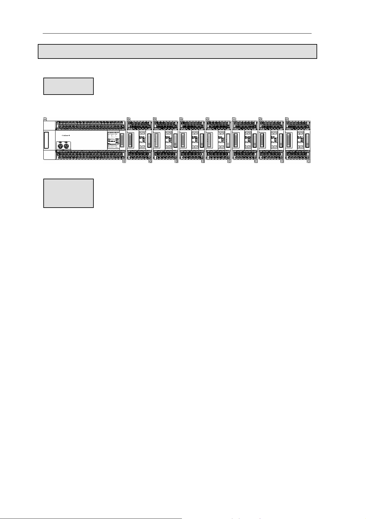
1-3. Expansion’s constitution and ID assignment
Expansion
• XC series PLC can be used independently or used along with
the expansions. The following is the chart of a basic unit with
seven expansions.
Constitution
Rules
• Digital Input/Output quantity is Octal
• Analogue Input/Output quantity is Decimal
• PLC main units can connect with 7 expansions and a BD
module. The input/output type is not limited, both switch and
analog quantity are available.
Summary of XC series PLC
10
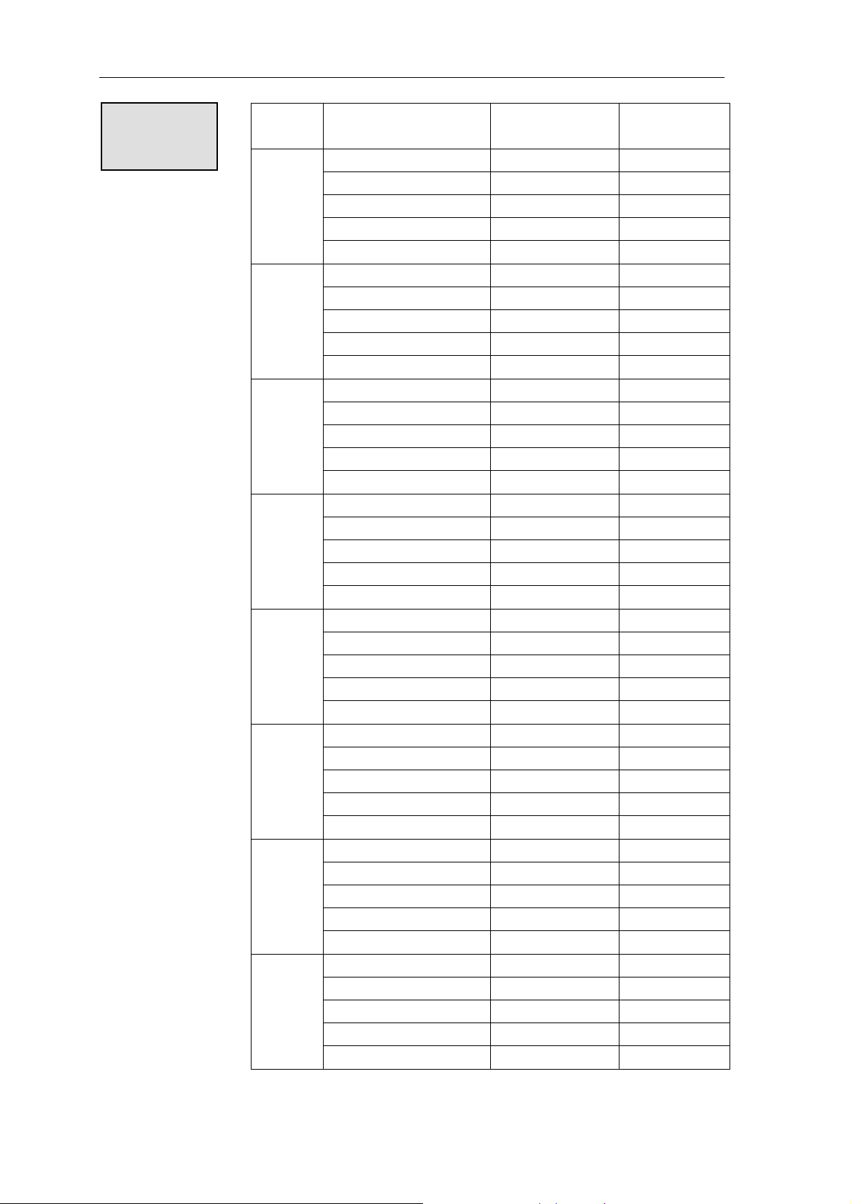
Summary of XC series PLC
ID
Assignment
Unit Type ID(As register)
Input switch quantity X X100~X137 32 points
Expansion
1#
Expansion
2#
Expansion
3#
Expansion
4#
Expansion
5#
Expansion
6#
Expansion
7#
BD Board
Output switch quantity Y Y100~Y137 32 points
Input analog quantity ID ID100~ID131 16 channels
Output analog quantity QD QD100~QD131 16 channels
Module’s set value D D8250~D8259 -
Input switch quantity X X200~X237 32 points
Output switch quantity Y Y200~Y237 32 points
Input analog quantity ID ID200~ID231 16 channels
Output analog quantity QD QD200~QD231 16 channels
Module’s set value D D8260~D8269 -
Input switch quantity X X300~X337 32 points
Output switch quantity Y Y300~Y337 32 points
Input analog quantity ID ID300~ID331 16 channels
Output analog quantity QD QD300~QD331 16 channels
Module’s set value D D8270~D8279 -
Input switch quantity X X400~X437 32 points
Output switch quantity Y Y400~Y437 32 points
Input analog quantity ID ID400~ID431 16 channels
Output analog quantity QD QD400~QD431 16 channels
Module’s set value D D8280~D8289 -
Input switch quantity X X500~X537 32 points
Output switch quantity Y Y500~Y537 32 points
Input analog quantity ID ID500~ID531 16 channels
Output analog quantity QD QD500~QD531 16 channels
Module’s set value D D8290~D8299 -
Input switch quantity X X600~X637 32 points
Output switch quantity Y Y600~Y637 32 points
Input analog quantity ID ID600~ID631 16 channels
Output analog quantity QD QD600~QD631 16 channels
Module’s set value D D8300~D8309 -
Input switch quantity X X700~X737 32 points
Output switch quantity Y Y700~Y737 32 points
Input analog quantity ID ID700~ID731 16 channels
Output analog quantity QD QD700~QD731 16 channels
Module’s set value D D8310~D8319 -
Input switch quantity X X1000~X1037 32 points
Output switch quantity Y Y1000~Y1037 32 points
Input analog quantity ID ID1000~ID1031 16 channels
Output analog quantity QD QD1000~QD1031 16 channels
Module’s set value D D8320~D8329 -
Max points/
Channels
11

1-4. General Specification
Summary of XC series PLC
General
Specification
Items Specifications
Insulate voltage Up to DC 500V 2MΩ
Anti-noise 1000V 1uS pulse per minute
Ambient
0°C~60°C
temperature
Ambient humidity 5%~95%
COM 1 RS-232, connect with host machine, HMI program or debug
COM 2 RS-232/RS-485, connect with network or aptitude instrument,
inverters etc.
COM 3 BD board COM port RS-232C/RS-485
COM 4 CANBUS COM port (XC5 series)
Installation Can use M3 screw to fix or install directly on DIN46277
(Width 35mm) orbit
Grounding The third type grounding (can’t public ground with strong
power system.)
12
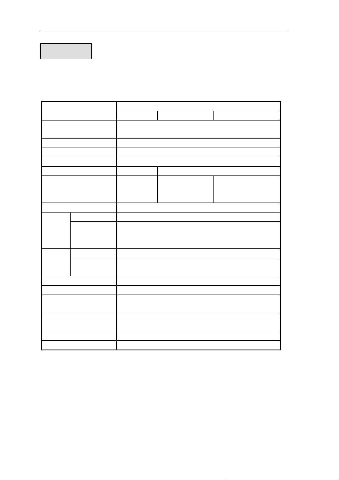
Performance
XC3 series:
Summary of XC series PLC
Item
Specification
14 points 24/32 points 48/60 points
Program executing
Loop scan format, time scan format
format
Program format Both statement and ladder
Dispose speed 0.5us
Power cut retentive Use FlashROM and Li battery
User program’s capacity 2500 steps 8000 steps
I/O points 8 I / 6 O Input 14/18 points
Output 10/14
Input 28/36 points
Output 20/24 points
points
Interior coil’s points (M) 8512 points
Points 620 points
Timer
(T)
Spec.
100mS timer: Set time 0.1~3276.7 seconds
10mS timer: Set time 0.01~327.67 seconds
1mS timer: Set time 0.001~32.767 seconds
Points 635 points
Counter
(C)
Spec.
16 bits counter: set value K0~32767
32 bits counter: set value K0~2147483647
Data Register(D) 8512 words
FlashROM Register(FD) 2048 words
High speed dispose
High speed count, pulse output, external interrupt
function
Setting of time scan
0~99mS
space
Password protection 6 bits ASCII
Self diagnose function Power on self-diagnose, Monitor timer, grammar check
13

1-5. Shape and Size
Exterior Size
XC1 series 16 points main units
XC3 series 14 points main units (Including 16 points expansions)
Summary of XC series PLC
XC1 series 32 points main units (Including 24 points main units)
XC3 series 24 / 32 points main units (Including 32 points expansions)
XC5 series 32 points main units
139
131
X21
X13
X15X7X6X5X4X3X2X1
X12
X14 X16
2 3540 1
76
X
PWR
RUN
XC3-32R-E
ERR
Y
104532
67
COM 4
Y10
Y11Y6Y7Y5COM 3Y12
X17
X20
Y13
Y15
Y14
5
.
3
110
102
94
COM
X0COM
FG
POR T2POR T1
0V
AY0COM 0
COM 2Y3
24V
COM 1
B
Y1
X11
X10
Y2
Y4
Xi n j e El e ct r oni c Co. , Lt d
SN :0067032266
73.3
D A T E :20060410
TYPE:XC3-32R-E
14

XC3 series 60 points main units (Including 48 points main units)
XC5 series 60 points main units (Including 48 points main units)
207.4
199.4
Summary of XC series PLC
73.3
102
94
X1
COM
X0
X2X3X4X5X6X7X10
COM
POR T 2POR T 1
CAN+ CAN-
0V
24V
B
A
X11
X13
X15
X17
X21
X23
X25
X12
X14
X16
X20
COM5
Y3
Y4
Y2Y1
Y0
COM3
COM 1CO M0
COM 2
COM 6
Y6COM4
Y5
X27
X22
X24
X26
X30
COM7
Y12Y7
Y10
Y15
Y13
Y11
Y16
Y14
X37
X35
X33
X31 X41
Y17
X34
X32
X
XC3-60R- E
Y
0
1326754
Y20
COM8
Y21
X40X36
4
5762 310
PWR
RUN
ERR
COM 9
Y22
Y23
Y24
X43
X42
Xi nj e El ec t r oni c Co. , Lt d
SN :0067032266
D A T E:20060410
TYPE:XC3-60R-E
Y27
Y25
Y26
15
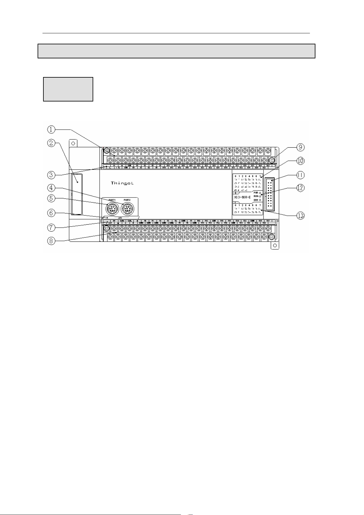
1-6. Terminal arrangement
Main Units
Summary of XC series PLC
1. Input terminals
2. BD expansion
3. Input label
4. COM port
5. COM port
6. COM port’s cover door
7. Output label
8. Output terminals
9. Screws
10. Input indicate LED
11. Extension port
12. Programming status indicate LED
13. Output indicate LED
16
XC3- 60 main units, XC5- 60 main units: 36 Input/24 Output
M
X21
X17
X15
X13
X11
X7
X5
X3
X1
CO M
COM
X14
X12
X10
X6
X4
X2
X0
X16
X20
X22
X23
Summary of XC series PLC
X27
X24
X25
X26
X30
X31
X32
X33
24V
0V
CAN+
CAN-
A
B
COM0COM1
Y1
Y0
COM2
Y2
COM3
Y4Y6COM5
Y3
COM4
Y5
COM6
Y10
Y11
Y12 COM7Y7
Y13
Y14 Y16
Y15
Y17
XC3- 48 main units, XC5- 48 main units: 28 Input /20 Output
X27
X25
X23
X21
X17
X15
X13
X11
X7
X5
X3
24V
X1
COM
CO M
0V
CAN+
CAN-
A
X0
B
X2
Y0
COM0COM1
X6
X4
Y1
Y2
COM2
X10
COM3
X12
Y4Y6COM5
Y3
COM4
X14
X16
Y5
X20
COM6
Y10
X22
Y11
Y12 COM7Y7
X24
Y13
X26
Y14 Y16
X31
X30
Y17
Y15 Y22
C1- 32 main units, XC3- 32 main units, XC5- 32 main units: 18 Input /14 Output
X
24V
0V
FG
CO M
CO M
CO M0
A
B
X1 X3 X5 X7 X1X13X11
X0 X2 X4 X6
Y0
CO M1
CO M2
Y1
Y2
Y3
Y4
CO M3Y5Y7Y6Y11
Y10
CO M4
5
X17
Y13
X21
X20
Y15
Y14
X16X14X12X10
Y12
C1- 24 main units, XC3- 24 main units: 14 Input /10 Output X
FG
CO M
CO M
X0
X1
X2
X3
X4
X5
X6
X11
X10
X12
X13
X15X7
X14
COM8
X32
COM8
Y20
X33
Y20
Y22
Y23
Y21
Y2
Y231
0V
24V
AY0CO M0
B
CO M1
Y1
CO M2
Y2
XC3- 14 main units: 8 Input /6 Output
CO M
FG
24V Y0 COM1Y3 Y5
0V
X1 X3 X5 X7
X6X4X2X0
A
Y4Y2Y1CO M0B
XC1- 16 main units: 8 Input /8 Output
CO
FG
24V Y0 COM1Y2 Y7
0V
CO M0
X1 X3 X5 X7
X6X4X2X0
Y5
Y4Y3Y1
Y6
Y3
Y4
Y5
CO M3
Y6
Y7
Y10
Y11
17
Expansions
XC-E8X8YR
Summary of XC series PLC
Y0
CO M 0
XC-E16X
CO M
CO M
XC-E16YR
Y0
CO M0COM1
CO M4
CO M
CO M
CO M1COM2Y3 Y4 Y6
CO M
CO M5COM6Y13 Y14 Y16
X0 X2 X4 X6
Y1
CO M
X11
Y1
Y11
X1 X3 X5 X7
X13 X15 X17
X16X14X12X10
CO M2Y3Y4Y6
X7X5X3X1
Y7Y5CO M3Y2
X6X4X2X0
Y7Y5CO M3Y2
Y17Y15CO M7Y12Y10
18
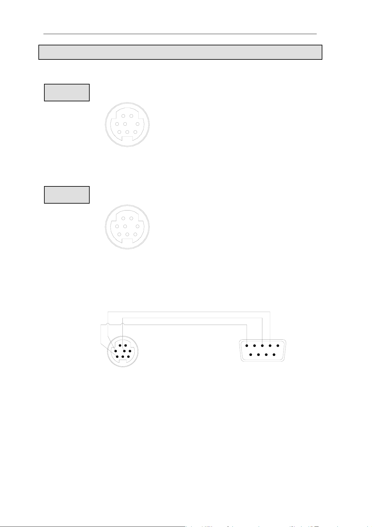
1-7. COM Port Definition
COM 1
Pin of COM 1
1
45
3
6
Mini Din 88 core socket (hole)
Summary of XC series PLC
2: PRG
备注
4: RxD
5: TxD
6: VCC
8: GND
2
8
7
COM 2
Pin of COM 2
4: RxD
1
45
3
6
2
8
7
5: TxD
8: GND
Mini Din 88 core socket (hole)
Connection of programmable cable is the following:
15
2
1
45
3
8
6
7
Mini Din 8 core socket (pin) DB9 pin (hole)
19

2-1. Power Specification
For the power specification of XC series programmable controller’s basic units, please see
the following table:
AC Power
Type
Rated voltage AC100V~240V
Voltage allow bound AC90V~265V
Rated frequency 50/60Hz
Allow momentary
power-cut time
Impact current Max 40A 5mS below/AC100V
Max power
consumption
Power for sensor use 24VDC±10% max 400mA
Interrupt time≤0.5 AC cycle, alternation≥1 sec
max 60A 5mS below /AC200V
12W
• To avoid voltage decrease, please use the power cable
thicker than 2mm2
• Even appear power cut within 10ms; PLC can still go on
working. But if long time power cut or abnormal power
decrease, PLC will stop working, output will also appear
OFF status, when recover power supply, the PLC will auto
start to work.
• Connect the grounding terminals of basic units and extend
modules together, then ground
DC power
type
Rated voltage DC24V
Voltage allow bound DC21.6V~26.4V
Input current
(Only basic unit)
Allow momentary
power-cut time
Impact current 10A DC26.4V
Max power
consumption
Power for sensor
use
120mA DC24V
10mS DC24V
12W
24VDC±10% Max 400mA
21

2-2. AC Power, DC Input Type
Constitution
and
Connection
Spec., Input/output and layout
·
• The Input power is connected between L and N terminals.
• 24+, COM terminals can be used to power 400mA/DC24V for sensor
·
supply. Besides, this terminal can’t be connected to external power.
• Terminal is NC terminal, please don’t go on exterior connection or
use it as relay terminal.
• Connect the basic unit with all expantions module’s COM terminal.
22
2-3. Input Specification
Basic Units
Input signal’s
voltage
Input signal’s
current
Input ON current Up to 4.5mA
Input OFF current Low than 1.5mA
Input response time About 10ms
Input signal’s
format
Circuit insulation Photo-electricity
Input action’s
display
Expansions
Input signal’s
voltage
Input signal’s
current
Input ON current Up to 4.5mA
Input OFF current Below 1.5mA
Input response time About 10ms
Input signal’s
format
Circuit insulation Photo-electricity
Input action’s
display
DC24V±10%
7mA/DC24V
Contact input or
NPN open collector
transistor
coupling insulation
LED light when
input ON
DC24V±10%
7mA/DC24V
Contacts input or
NPN open collector
transistor
coupling insulation
LED light when
input ON.
Spec., Input/output and layout
23
2-4. DC Input Signal’s Disposal(AC Power Type)
DC input signal
Spec., Input/output and layout
z Input terminal
When connect input terminal and COM terminal with contacts without voltage or
NPN open collector transistor, if input is ON,LED lamp lights, which indicates input。
There are many COM terminals to connect in PLC.
z Input circuit
Use optical coupling instrument to insulate the input once circuit and twice circuit,
There’s a C-R filter in the twice circuit。It is set to avoid wrong operation caused by
vibration of input contacts or noise along with input signal. As the preceding reason, for
the changing of input ON→OFF,OFF→ON,in PLC, the response time delays about
10ms。There’s a digital filter inside X000~X015。This kind of filter can very from
0~15ms according to the special register (D8020).
z Input sensitive
The PLC’s input current is DC24V 7mA,but to be safe,it needs current up to 3.5mA
when it’s ON,lower than 1.5mA when it’s OFF.
24
Spec., Input/output and layout
Exterior
circuit used
Input Connection
XC series PLC’s input power is supplied by its interior 24V power,so if
use exterior power to drive photoelectricity sensor etc., this exterior
power should be DC24V±4V,please use NPN open collector type for
sensor’s output transistor
25
Spec., Input/output and layout
2-5. Output Specifica
Relay output
Interior power Be
Circuit insulation ion Mechanism insulat
Action deno mp te LED indicate la
Max
load
Open circuit’s leak
current
Mini load DC5V 2mA
me
ti
Interior power Below DC5~30V
Circuit insulation Optical coupling
Action denote Indicate lamp LED
Max
load
Resistant
load
Induce load 80VA
Lamp load 100W
OFF→ON 10ms Response
ON→OFF 10ms
Transistor Output
Restance
load
Induce load 12W/DC24V
tion
low AC250V, DC30V
3A
-
insulation
0.8A
Lamp load 1.5W/DC24V
Open circuit’s leak
urrent
c
Mini load DC5V 2mA
OFF→ON Below 0.2ms Response
time
ON→OFF Below 0.2ms
-
26
Spec., Input/output and layout
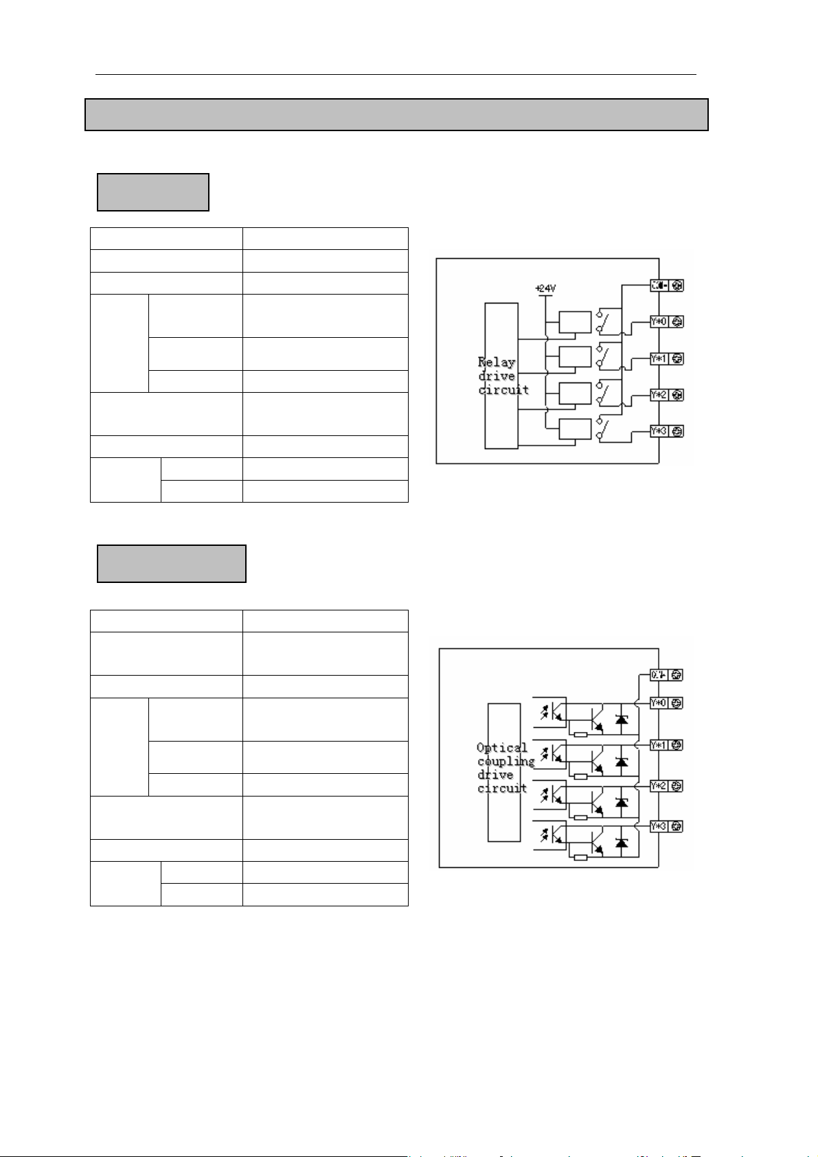
2-6. Disposal of Relay Output Circuit
Relay output circuit
z Output terminals
Relay output type includes 2~4 public terminals. So each public-end unit can drive different
power-voltage system’s (E.g.:AC200V,AC100V,DC24V etc.) load.
z Circuit’s insulation
Between the relay output coils and contacts,PLC’s interior circuits and exterior circuits, load
circuits are electric insulation. Besides, each public-end blocks are separate.
z Action display
LED lamp lights when output relay’s coils galvanize, output contacts are ON.
z Response time
From the output relay galvanize (or cut) to the output contacts be ON (or OFF), the response time is
about 10ms
z Output current
The current-voltage below AC250V can drive the load of pure resistace 2A/1 point、inductance load
below 80VA(AC100V or AC200V) and lam load below 100W(AC100V or AC200V).
z Open circuit’s leak current
When the output contact be OFF and there’s no leak current,can directly drive Ne lamp etc.
z The life of relay output contacts
Standard life of induce AC load such as cont ctor、electromagnetism valve:5 million times for
20VA load. Cut power device’s life according t the company’s test: for 80VA load, the action life is
up to 2 million times. But if the load parallel nnect with surge absorber, the life will be greatly
improved!
Output connection example
p
a
o
co
27

Spec., Input/output and layout
Constitution
of output
circuit
DC load
AC load
z For DC induce load, please parallel connect with commutate diode.
If not connect with the commutate diode, the contact’s life will be
decreased greatly. Please choose the commutate diode which allow
inverse voltage endurance up to 5~10 times of the load’s voltage,
ordinal current exceeds load current.
z Parallel connect AC induce load with surge absorber can reduce
noise.
28
Spec., Input/output and layout
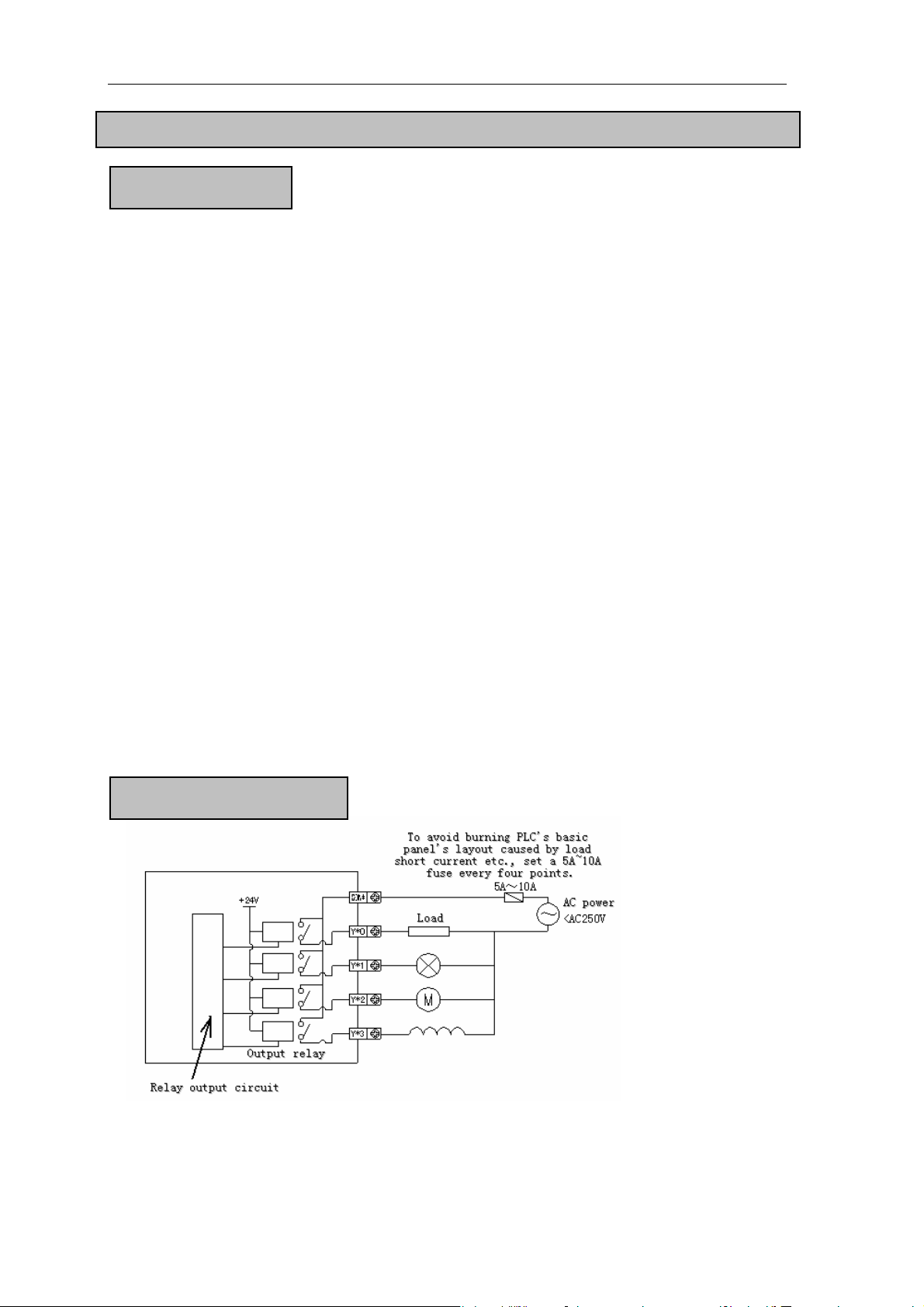
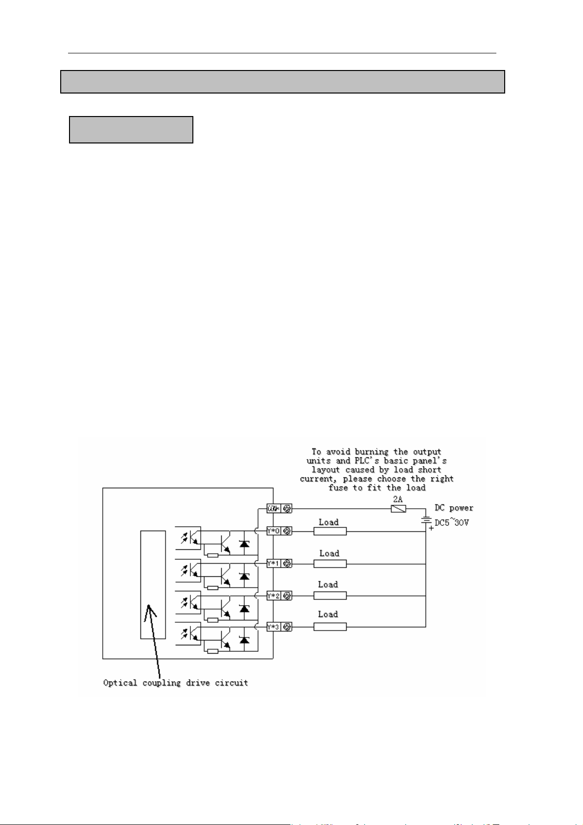
2-7. Disposal of Transistor Output Circuit
Transistor output circuit
¾
z Output terminal
Basic unit’s transistor output has 1~4 public-end output.
z Exterior power
Please use DC5~30V steady-voltage power for load drive,
z Circuit insulation
Use photoelectricity coupling device to insulate PLC’s interior circuit and output
transistor. Besides, each public block is separate.
z Action denote
When drive optical coupling,LED lights,output transistor is ON.
z Response time
From photoelectricity coupling device drive (or cut) to transistor ON (or OFF), the time
PLC uses is below 0.2ms.
z Output current
The current is 0.5A per point。But as restrict by temperature goes up, the current is 0.8A
every four points.
z Open circuit’s current
Below 0.1mA
29


3. Each Soft Unit’s Usage and Function
T his chapter, we’ll give some description of the PLC’s data and the function of interior input/output relay, auxiliary
lay, status, counter, data register etc. This item is the base to use PLC. re
3-1.Every Soft Unit of PLC
3-2.Soft Unit’s ID List
3-3.Disposal of Data
3-4.Some Encode Principle of Soft Units
3-5.Timer’s ID and Function [T]
3-6.Counter’s ID and Function [C]
3-7.Note Items
31

Function of each device
3-1. Every Soft Unit of Programmable Controller
In the programmable controller, there are many relays、timers and counters,they all have
countless “a” contacts(Normally open contacts)and “b” contacts(Normally closed contacts),
Connect these contacts and coils to constitute sequencial control circuit. The following, we’ll
briefly introduce each soft unit:
【Input(X)and output(Y)relay】
z In each basic unit, assign the ID of input relay, output relay in the format of
X000~X007,X010~X017…,Y000~Y007,Y010~Y017… this octal format. The ID of
extension is connected behind basic unit.
z The ID of expansion obeys the principle of channel 1 starts from X100/Y100, channel 2
starts from X200/Y200… 7 expansions could be connected totally.
z Use digital filter in the special input filter of input relay, so you can use the program to
change the sieve value. So in the high-speed receive application, you can assign this type
of relay’s ID No.
【Auxiliary relay(M)】
z Auxiliary relay is the relay inside the programmable controller,this type of output relay
is different from input/output relay,it can’t gain exterior input,it also can’t drive exterior
load,it can only be used in the program。
z The relay used for retentive can still save its ON/OFF status in the case of PLC power
cut.
【Status(S)】
z Relay used as step ladder chart.
z When not used as working procedure No.,it’s the same with auxiliary relay and can be
used as common contact/coil to carry on programming. Besides, it can also be signal
alarm to diagnose exterior trouble.
【Timer(T)】
z Timer could carry on plus operation to 1ms,10ms,100ms etc. time pulse in PLC, When
reach certain set value, output contact act.
z T100~T199 are timers with the unit of 100ms clock pulse,their current values are the
accumulate values. So, even though timer coil’s drive input is cut, they will still hold the
current value, go on accumulating the action.
32

Function of each device
【Counter(C)】
z The counters can be divided into the following sorts according the their usage and
purpose:
[Used for interior count] Common use / power failure retentive use
16 bits counter:Used for plus count,count bound: 1~32,767
32 bits counter:Used for add / minus count,count bound: -2,147,483,648~+2,
147,483,647
These counters are used for PLC’s interior signals, usually their response speed is below
10Hz.
[Used for high-speed count] For power failure retentive use
32 bits counter: For plus / minus count, count bound: -2,147,483,648~+2,147,483,6487
(Single phase plus count,single phase plus/minus count,AB phase
count) allocate to the special input points.
High-speed counter can count with the frequency below 200kHz,independent with the
PLC’s scan cycle.
【Data register(D)】
z Data register is the soft unit used by data register to save data. XC series PLC’s data
registers are all 16 bits (The high bit is the sign bit), Combine two registers can carry on
32 bits data disposal (The high bit is the sign bit).
Just the same with other soft units, data registers can also be divided to be two types: for
common use and power failure retentive use.
【Constant(K)、(H)】
z In the diverse value used by PLC, K means decimal integer,H means Hex. Value. They
are used to be the set value and current value for the timer and counter, or applied
instructions’ operands.
【Pointer(P)(I)】
z Pointers are used for branch and interrupt. The pointer (P) used by branch is the jump
aim used for condition jump or subroutine jump. Pointer used for interrupt is used for the
assigned input interrupt, time interrupt.
33

3-2. Device’s ID List
For the allocate of device’s ID, please see the following list:
Besides, when connect input / output expansions and special expansions on the basic units, for
the input / output relay’s No., please refer to the user manual.
Mnemonic Name
X Input relay X000~X007
Y Output relay Y000~Y005
M Interior relay
S Flow
T Timer
C Counter
D Data Register
FD
FlashROM
Register
Bound points
14 points 24\32 points 48 \60 points
X000~X015
X000~X021
Y000~Y011
Y000~Y015
M0~M2999【M3000~M7999】 8000
M8000~M8511 for special using 512
S0~S511
【S512~S1023】
T0~T99:100ms not accumulation
T100~T199:100ms accumulation
T200~T299:10ms not accumulation
T300~T399:10ms accumulation
T400~T499:1ms not accumulation
T500~T599:1ms accumulation
T600~T618:1ms with interruption precise time
C0~C299:16 bits forth counter
C300~C598:32 bits forth/back counter
C600~C634:high-speed counter
D0~D3999
【D4000~D7999】
For special usage D8000~D8511 512
FD0~FD1535 1536
For special usage FD8000~FD8511 512
X000~X033
X000~X043
Y000~Y023
Y000~Y027
Function of each device
14
24\32
points
8 points
6 points
points
14\18
points
10\14
points
1024
620
635
8000
48 \60
points
28\36
points
20\24
points
34

Function of each device
NOTE:
※1. The memorizer area in 【 】 is the defaulted power failure retentive area;soft
elements D、M、S、T、C can be set to change the power failure retentive area. For the
details, please see the following table
※2. FlashROM register needn’t set power failure retentive, its data won’t lose when power is
cut (No battery).
※3. The serial No. of input coil、output relay are octal data, other memorizers’ No. are all
algorism data.
Setting of soft unit’s power failure saving area:
Mnemonic Set area Function
D FD8202
M FD8203
T FD8204
C FD8205
S FD8206
Start denotation of D power
cut save area
Start denotation of M power
cut save area
Start denotation of T power
cut save area
Start denotation of C power
cut save area
Start denotation of S power
cut save area
System’s
defaulted
value
4000 D4000~D8000
3000 M3000~M8000
620 Not set
320 C320~C640
512 S512~S1024
Memory bound
of power drop
35

Function of each device
3-3. Data Disposal of Programmable Controller
According to different usage and purpose, XC series programmable controllers use 5 types of
count format. For their usage and function, see the following:
《DEC》(DEC:DECIMAL NUMBER)
¾ The set value of timer and counter(K constant)
¾ The ID of auxiliary relay(M),timer(T),counter(C),status(S)(Soft
unit’s number)
¾ Assign the value in the operands and instruction’s action(K constant)
《HEX》(HEX:HEXADECIMAL NUMBER)
¾ The same with DEC data,it is used to assign the value in the operands and
instruction’s action(H constant)
《BIN》(BIN:BINARY NUMBER)
¾ Just as said before,carry on data allocation to timer, counter or data register in
the format of DEC. or Hex., But in the PLC, these data are all be put in the
format of binary data. And, when carry on monitor on the peripherial device,
these soft units will auto switch to be DEC. data as shown in the graph.(they
can also switch to be Hex. Data.).
《OCT》(OCT:OCTAL NUMBER)
¾ The input relay, output relay’s soft units’ ID of XC series PLC are allocate in
the format of OCT data. So, it can go on carry of [1-7,10-17,...70-77,
100-107].
《BCD code》(BCD: BINARY CODE DECIMAL)
¾ BCD is the method which use 4 bits binary to denote decimal 0~9. It’s easy to
despose bit. So, BCD is available to denote digital switch or 7 segments display
control.
《Other data(float)》
¾ XC series PLC has the function of high precision floating point operation. Use binary
floating point data to execute floating point operation, use decimal floating value to
execute monitor.
36

3-4. Some encode principles of device
1、Data register could be used as offset(indirect assignment)
Format:Dn[Dm]、Xn[Dm] 、Yn[Dm] 、Mn[Dm] etc.
Function of each device
M8002
M2
M8000
MOV K0 D0
MOV K5 D0
MOV D10[D0] D100
Y0[D0]
In the preceding example, when D0=0, then D100=D10, Y0 is ON;
z Word’s offset composed by bit soft units:DXn[Dm] means DX[n+Dm];
z Soft units with offset, the offset could only be denoted with soft device D.
When M2 turns from OFF to be ON, D0=5, then D100=D15, Y5 is ON.
When D10[D0]=D[10+D0], Y0[D0]=Y[0+D0].
2、 Bit units compose word
Input X、output Y、middle coil M could compose 16 bits word. E.g. DX0 means
X0~X17compose to be a 16 bits data. DX20 means X20~X37 combines a 16 bits data.
Format:Add a D before bit device
Bit devices combine to be word devices:DX、DY、DM、DS、DT、DC
M0
M1
M8000
MOV K21 DY0
MOV K3 D0
MOV DX2[D0] D10
In the preceding example, when M0 turns from OFF to be ON, the value of the word DY0 composed
by Y0~Y17 equals 21,i.e. Y0、Y2、Y4 turns to be ON status.
Before M1 be activate, when D0=0, DX2[D0] means a word composed by X2~X21;
When M1turns from OFF to be ON, D0=3, then DX2[D0] means a word composed by X5~X24
z DXn(the bound of “n” is the exact bound of “X”),choose 16 points from the head to the end,
add 0 if not enough.
z Please note, the word composed by bit device couldn’t carry on bit searching address.
37

Function of each device
3、 Bit of word device
Format:Dn.m
Register could carry on bit searching address, e.g. Dn.m means number “m” bit of Dn data
register(0≤m≤15)。
D0.4
Y0
D5[D1].4
Y1
In the preceding example, D0.4 means when the No.4 bit of D0 is 1, Y0 set ON;
D5[D1].4 means bit searching address with offset, if D1=5,it says D5[D1] means the number 4
bit of D10.
z The bit of word device with offset is denoted as Dn[Dm].x
z Please note, to the bit of word device, they couldn’t combined to be word device.
4、 T/C means the difference of register’s word and bit
To T and C register, Tn/Cn means be a bit register or a word register should be
distinguished by the instructions.
T、C could denote the status of timer、counter, or the current value of time、counter, it is
distinguished by the instructions.
X0
T11
K99
M0
T11
MOV D0T11
Y1
In the preceding example,MOV T11 D0,T11 means word register;
LD T11,T11 means bit register.
5、 Tag type:P,I
e.g.:P means the tag which using CJ instruction or CALL instruction which could jump; I
means interrupt tag.
38

3-5. Timer’s Number and Function [T]
Timer’s number
100ms not accumulated(16 bits) T0~T99
100ms accumulated(16 bits) T100~T199
10ms not accumulated(16 bits) T200~T299
10ms accumulated(16 bits) T300~T399
1ms not accumulated(16 bits) T400~T499
1ms accumulated(16 bits) T500~T599
Function
The timer accumulates clock pulse of 1ms,10ms,10ms inside PLC. When
reach the set value, the output contact activates.
The common timers don’t set exclusive instructions, use OUT instruction
to time; use constant K in the program memory, also you could use
register’s content (D) to indirect assign.
Please see the following table for the timer’s [T] number (the
number is assigned according to Hex.)
Function of each device
Common format Accumulation format
If drive input X000 of time coil T200
is ON, T200 accumulates 10ms clock
pulse with the current value timer. If
this current value equals the set value
K200, timer’s output contact activates.
That is, output contact activates after 2
seconds of coil driving. Driving input
X000 cut or power cut, timer reset,
output contact reset.
If the drive input X001 of timer’s coil
T300 is ON, T300 accumulates 10ms
clock pulse with the current value
counter. When the value reaches the set
value K2000, counter’s output contact
activates. In the count process, even the
input X001 cut or drop power, when start
again, go on counting, its accumulation
time is 20 seconds. When reset input
X002 is ON, timer reset, output contact
reset.
39

Assign
method of
the set value
The Time
Value
Action
Function of each device
《Constant assignment (K)》
X0
T10 K100
T10 is a timer with the unit of
100ms. Assign 100 as a constant,
then 0.1s×100=10s timer work.
《Indirect assignment (D)》
X0
MOV K200 D5
X1
T10 D5
Write content in indirect data register
to program or input via data switch.
When assigned as power cut retentive
register, please note that voltage low
will cause the set value instable.
The count format of Timers T0~T599 is 16 bits linear increment mode
(0~K32 ,767). If the timer’s count value reaches the maximum value K32767,
the timer will stop timing , the timer’s status will remain the same status.
《Output delay on-off timer》
X0
Y0 X0
T2
Y0
T2
K200
X0
Y0
T2
When X000 is ON, output Y000;
If X000 changes from ON to be OFF, T2(20 seconds)will be delayed, the will
n
output Y000 cut.
《Flicker》
X0
T1
If X000 activates, Y000 starts flicker output.
T1 controls the OFF time of Y000, T2 controls the ON time of Y000.
T2
T1
T2
Y0
K20
K10
X0
T1 T2 T1
Y0
40

Function of each device
3-6. Counter’s ID and
Counter’s ID
Counter’s
characters
Items 16 bits counter 32 bits counter
Count direction Positive Positive/negative
The set value 1~32,767 -2,147,483,648~+2,147,483,647
The assigned set
value
Changing of the
current value
Output contact
Reset activates
The current value
register
For the counter’s number (C), ple r to the following table: ase refe
function [C]
16 bits positive counter 299
32 bits positive/negative
counter
High speed counter
The characters of 16 bits counter and 32 bits counter are shown below:
Constant K or data
register
Change after positive
count
Hold the action after
positive count
When executing RST command,counter’s current value is 0,
output contacts recover
16 bits 32 bits
C0~C
C300~C598 (C300, C302...C598) (Each one
engrosses 2 counter No.) The number must be
even.
C600~C634(C600,C602...C634) (Each one
engrosses 2 counter No.) The number must be
even
Same as the left, but data register
must be in a couple
Change after positive count (Loop
counter)
Hold the action after positive count,
reset if negative count
41

Function of each device
Function
About the assignment of normally used counter and power failure retentive
counter, they could be changed in the method of changing FD parameters’
settin via the peripheral device. g
16 bits counter For normally use or power count r etentive
16 bits binary increment counter, its valid setting value is K1~K32,767
(Decimal constant). The set value K0 and K1 have the same meaning, i.e. act
when output contacts at the beginning of first time count.
If cut the PLC’s power, then the value
X0
RST C0
X1
C0 K10
of the normally use counter will be
reset. However, counter used by power
cut retentive could save the count
value after power cut, and the counter
will go on counting from the value.
C0
Y0
z Every time when X001 drives coil C0, the counter’s current value will
increase. When execute the coil instruction the tenth time, output contact
acts. Later, even X001 activates, counter’s current value will not change.
z If reset input X000 is ON, execute RST instruction, counter’s current
value is 0, output contacts activates.
z For the counter’s set value, it could not only set by constant K, but also be
assigned by data register’s ID. E.g. assign D10, if the content of D10 is
123, it’s the same with setting K123.
z When write the set value to the current value register via MOV instruction
etc. When input next time, output coil gets, current value register turns to
the set value.
42

Function of each device
32 bits counter For normally use or power count r etentive
Assign
method of
the set value
For 32 bits binary increment counter, its valid bound is K1~K2,147,483,647
(Decimal constant). With special auxiliary relay M8238, assign the direction of
bits positive/negative counter’s (C300~C498) direction
z If X2 drives M8238, then it is
negative count;If no drive, then it is
X2
M8238
X3
RST C300
X4
C300 K10
positive count.
z According to constant K or to the
content of data register D, set the
value to be positive. Treat contents
in consecutive data register as a
pair, and dispose it as 32 bits data.
So, when assign D0, dispose D0
C300
Y1
and D1 as a 32 bits set data. If use
count input X004 to drive coil
C300, execute increase count.
z When reset input X3 is ON, execute RST instruction, counter’s current
value turns to be 0, output contact resets.
z When use counter as power cut retentive, counter’s current value, output
contact’s action and reset status cut power retentive.
z 32 bits counter can also be used as 32 bits data register. But 32 bits data
register can’t be used as device in 16 bits applied instructions.
16 bits counter
《Constant assignment(K)》
X001
C0
K100
《Indicate assignment(K)》
X000
X001
MOV K100 D5
C0 D5
43

Function of each device
32 bits counter
《Constant assignment(K)》
The count
value
X001
C300
K43,100
《Indicate assignment(K)》
X000
X001
DMOV K43100 D0
C300
D0
( D1)
The count mode of counters T0~T599 is 16 bits linear increment mode
(0~K32767). When counter’s count value reaches the max value K32767, the
counter will stop counting, the counter’s status will remain.
44

Function of each device
3-7. Some Points to Note
Action order of input/output relay and response delay》
《
Input disposal
Before PLC executing the program, read all the input terminal’s ON/OFF status of PLC to
the image area. In the process of executing the program, even the input changed, the content
in the input image area will not chang
read out the change.
Output disposal
Once finish executing all the instructions, transfer the ON/OFF status of output Y image
area to the output lock memory area. This will be the actual output of the PLC. The
contacts used for the PLC’s exterior output will act according to the device’s response
delay time.
When use this input/output f
filter and output device will also appear response delay.
ormat in a batch, the drive time and operation cycle of input
e. However, in the input disposal of next scan cycle,
《Not accept narrow input pulse signal》
PLC’s input ON/OFF time should be longer than its loop time. If consider input filter’s
response delay 10ms, loop time is 10ms,then ON/OFF time needs 20 ms separately. So, up to
1,000/(20+20)=25Hz input pulse can’t be disposed. But, this condition could be improved
when use PLC’s special function and applied instructions.
Dual output(Dual coils)action》
《
X1
Y3
X2
Y3
Y4
Y3
When executing dual output (use dual coil),
the back side act in prior
As shown in the left map, please consider
the things of using the same coil Y003 at
many positions:
E.g. X001=ON,X002=OFF
At first, X001 is ON, its image area is ON,
output Y004 is also ON.
But, as input X002 is OFF, the image area
of Y003 is OFF.
So, the actual output is : Y003=OFF,
Y004= ON.
45

4. Basic Program Instructions
In this chapter, we tell some basic instructions and their functions.
4-1.List of Basic Instructions
4-2.【LD】,【LDI】,【OUT】
4-3.【AND】,【ANI】
4-4.【OR】,【ORI】
4-5.【LDP】,【LDF】,【ANDP】,【ANDF】,【ORP】, 【ORF】
4-6.Compare Instructions
4-7.【ORB】
4-8.【ANB】
4-9.【MCS】,【MCR】
4-10.【ALT】
4-11.【PLS】, 【PLF】
4-12.【SET】, 【RST】
4-13.【OUT】, 【RST】 (Compare with counter’s soft unit)
4-14.【NOP】, 【END】
4-15.Note Items When Programming
46

4-1. List of Basic Instructions
XC1, XC3, XC5 series basic SFC instructions
Mnemonic Function Format and Device
LD
(LoaD)
LDI
(LoaD Inverse)
LDP
(LoaD Pulse)
LDF
(LoaD Falling Pulse)
AND
(AND)
ANI
(AND Inverse)
ANDP
(AND Pulse)
ANDF
(AND Falling pulse)
OR
(OR)
ORI
(OR Inverse)
ORP
(OR Pulse)
ORF
(OR Falling pulse)
ANB
(ANd Block)
ORB
(OR Block)
OUT
(OUT)
SET
(SET)
RST
(ReSeT)
PLS
(PuLSe)
PLF
(PuLse Falling)
Initial logical operation contact
type NO (normally open)
Initial logical operation contact
type NC (normally closed)
Initial logical operation-Rising
edge pulse
Initial logical operation-Falling
/trailing edge pulse
Serial connection of NO
(normally open) contacts
Serial connection of NC
(normally closed) contacts
Serial connection of rising edge
pulse
Serial connection of
falling/trailing edge pulse
Parallel connection of NO
(normally open) contacts
Parallel connection of NC
(normally closed) contacts
Parallel connection of rising edge
pulse
Parallel connection of
falling/trailing edge pulse
Serial connection of multiply
parallel circuits
Parallel connection of multiply
parallel circuits
Final logic operation type coil
drive
Set a bit device permanently ON Y, M, S, T, C, Dn.m
Reset a bit device permanently
OFF
Rising edge pulse X, Y, M, S, T, C, Dn.m
Falling/trailing edge pulse X, Y, M, S, T, C, Dn.m
Basic SFC Functions
X, Y, M, S, T, C, Dn.m, FDn.m
X, Y, M, S, T, C, Dn.m, FDn.m
X, Y, M, S, T, C, Dn.m, FDn.m
X, Y, M, S, T, C, Dn.m, FDn.m
X, Y, M, S, T, C, Dn.m, FDn.m
X, Y, M, S, T, C, Dn.m, FDn.m
X, Y, M, S, T, C, Dn.m, FDn.m
X, Y, M, S, T, C, Dn.m, FDn.m
X, Y, M, S, T, C, Dn.m, FDn.m
X, Y, M, S, T, C, Dn.m, FDn.m
X, Y, M, S, T, C, Dn.m, FDn.m
X, Y, M, S, T, C, Dn.m, FDn.m
None
None
Y, M, S, T, C, Dn.m
Y, M, S, T, C, Dn.m
47

Basic SFC Functions
MCS
(New bus line start)
MCR
(Bus line return)
ALT
(Alternate state)
NOP
(No Operation)
END
(END)
Connect the public serial contacts None
Clear the public serial contacts None
The status of the assigned device
X, Y, M, S, T, C, Dn.m
is inverted on every operation of
the instruction
No operation or null step None
Force the current program scan to
None
end
48

4-2. 【LD】,【LDI】,【OUT】
Mnemonic
Mnemonic Function Format and Devices
LD
(LoaD)
Initial logic operation
contact type NO (Normally
Open)
LDI
(LoaD Inverse)
Initial logic operation
contact type NC (Normally
Closed)
OUT
(OUT)
Final logic operation type
drive coil
Basic SFC Functions
Devices: X, Y, M, S, T, C, Dn.m,
FDn.m
M0
Devices: X, Y, M, S, T, C, Dn.m,
Dn.m F
D
evices: X, Y, M, S, T, C, Dn.m,
FDn.m
Statement
z Connect the LD and LDI instructions directly to the left bus bar. Or use
them to define a new block of program when using ANB instruction.
z OUT instruction is the coil drive instruction for the output relay、
auxiliary relay、status、timer、counter. For the input relay, cannot use.
z Can not sequentially use parallel OUT command for many times.
z For the timer’s time coil or counter’s count coil, after using OUT
instruction, set constant K is necessary.
z For the constant K’s set bound、actual timer constant、program’s step
relative to OUT instruction(include the set value)
See the following table
r Setting bound of K Timer/Counte The actual set value
1ms timer 0.001~32.767 seconds
1~32,767
10ms timer 0.01~32.767 seconds
100ms timer
0.1~32.767 seconds
16 bits counter 1~32,767 Same as the left
32 bits cou ter 1~2,147,483,647 Same as the left n
49

Basic SFC Functions
X0
Program
X1
T0
-3. 【AND】,【ANI】
4
Mnemonic Function Format and Devices
Mnemonic
AND
(AND)
ANI
(ANd Inverse)
Y100
M1203
T 0
Y 1
Serial connection of
NO (Normally Open)
contacts
Serial connection of
NC (Normally Closed)
contacts
K19
Devices
Devices
LD X0
OUT Y100
LDI X1
OUT M120
3
OUT T0
SP K19
LD T0
OUT Y1
M0
: X, Y, M, S, T, C, Dn.m, FDn.m
M0
: X, Y, M, S, T, C, Dn.m, FDn.m
Description
Program
z Use the AND and ANI instructions for serial connection of contacts.
As many contacts as required can be connected in series. They can
be used for many times.
z The output processing to a coil, through writing the initial OUT
instruction is called a “follow-on” output (For an example see the
program below: OUT M2 and OUT Y003). Follow-on outputs are
permitted repeatedly as long as th
no limit for the serial connected
e output order is correct. There’s
contacts’ No. and follow-on outputs’
number.
X2 M1
X3Y2
T1
Y2
M2
Y3
LD X2
AND M1
OUT Y2
LD Y2
ANI X3
50

4-4. 【OR】,【ORI】
Mnemonic
and
Function
Mnemonic Function Format and Devices
OR
(OR)
ORI
(OR Inverse)
Description
z Use the OR and ORI instructions for parallel connection of contacts.
z OR and ORI start from the instruction’s step, parallel connect with the
Basic SFC Functions
Parallel connection of
NO (Normally Open)
contacts
Devices: X, Y, M, S, T, C, Dn.m, FDn.m
Parallel connection of
NC (Normally Closed)
contacts
Devices: X, Y, M, S, T, C, Dn.m, FDn.m
To connect a block that contains more than one contact connected in
series to another circuit block in parallel, use an ORB instruction.
LD and LDI instruction’s step said before. There is no limit for the
parallel connect times.
Program
LD X5
OR X6
OR M11
OUT Y6
LDI Y6
AND M4
OR M12
ANI X7
OR M13
51

Basic SFC Functions
Relationship
with ANB
M11
M12
M13
X5
X6
Y6 M4 X7
Y6
M100
The parallel connection with
OR, ORI instructions should
connect with LD, LDI
instructions in principle. But
after the ANB instruction,
it’s available to add a LD or
LDI instruction.
4-5. 【LDP】,【L 【AND P ,【ORF】
DF】, P】,【ANDF】,【OR 】
52

Mnemonic
and
Function
Description
Program
Basic SFC Functions
Mnemonic Function Format and Devices
LDP
(LoaD Pulse)
Initial lo
operation-Rising edge
gical
pulse
Devices: X, Y, M, S, T, C, Dn.m, FDn.m
LDF
(LoaD Falling
pulse)
ANDP
(AND Pulse)
Initial logical
operation
Falling/trailing edge
pulse
Devices: X, Y, M, S, T, C, Dn.m, FDn.m
Serial connection of
Rising edge pulse
Devices: X, Y, M, S, T, C, Dn.m, FDn.m
ANDF Serial connection of
(AND Falling
pulse)
ORP
(OR Pulse)
ORF
(OR Falling
pulse)
Falling/trailing edge
pulse
Parallel connection of
Rising edge pulse
Parallel connection of
Falling/trailing edge
pulse
Devices: X, Y, M, S, T, C, Dn.m, FDn.m
Devices: X, Y, M, S, T, C, Dn.m, FDn.m
Devices: X, Y, M, S, T, C, Dn.m, FDn.m
z LDP、ANDP、ORP are active for one program scan after the
associated devices switch from OFF to ON.
z LDF、ANDF、ORF are active for on
associated devices switch from ON to
X5
X6
M8000 X7
M13
M15
e program scan after the
OFF.
LDP X5
ORP X6
OUT M13
LD M8000
ANDP X7
OUT M15
X5
X6
M8000 X7
M13
M15
In the preceding chart, when X005~X007 turns from ON t OFF or
om OFF to ON, M13 or M15 has only one scan cycle activates.
fr
o
LDF X5
ORF X6
OUT M13
LD M8000
ANDF X7
OUT M15
53

Basic SFC Functions
Output drive
In two conditions, when X0 turns from OFF to ON, M20 gets a scan cycle.
NOTE:
X10
X10
MOV
MOV
K10 D0
K10 D0
When X10 turns from OFF to ON,
only execute once MOV instruction.
When X10 turns from OFF to ON,
each scan cycle execute once MOV
instruction.
54

4-7. 【ORB】
Mnemonic
and
Function
Description
Basic SFC Functions
Mnemonic Function Format and Devices
ORB
(OR Block)
Parallel connection of
multiply parallel circuits
Devices: none
z To declare the starting point of the circuit (usually serial circuit blocks)
to the preceding circuit in parallel. Serial circuit blocks are those in
which more than one contacts in series or the ANB instruction is used.
z An ORB instruction is an independent instruction and is not associated
with any device number.
z There are no limitations to the number of parallel circuits when using an
ORB instruction in the sequential processing configuration.
z When using ORB instructions in a batch, use no more than 8 LD and
LDI instructions in the definition of the program blocks (to be
connected parallel).
Program
Recommended sequencial
programming method:
LD X0
AND X1
LD X2
AND X3
ORB
LDI X4
AND X5
ORB
Non-preferred batch
programming
method:
LD X0
AND X1
LD X2
AND X3
LDI X4
AND X5
ORB
55

4-8. 【ANB】
Mnemonic
Description
Basic SFC Functions
Mnemonic Function
ANB
(ANd Block)
Serial connection of
multiply parallel circuits
Format and Devices
Devices: none
z To declare the starting point of the circuit block, use a LD or LDI
instruction. After completing the parallel circuit block, connect it to the
preceding block in series using the ANB instruction.
z It is possible to use as many ANB instructions as necessary to connect a
number of parallel circuit blocks to the preceding block in series. When
using ANB instructions in a batch, use no more than 8 LD and LDI
instructions in the definition of the program blocks (to be connected in
parallel)
Program
Start of a branch
Start of a branch
End of a parallel circuit block
End of a parallel circuit block
Serial connect with the preceding circuit
LD X0
OR X1
LD X2
AND X3
LDI X
AND
X5
ORB
4
OR X6
ANB
OR X7
OUT Y20
56

4-9. 【MCS】,【MCR】
Mnemonic
Mnemonic
MCS
(Master control)
MCR
(Master control
Reset)
Description
z After the execution of an MCS instruction, the bus line(LD、LDI)shifts
to a point after the MCS instruction. An MCR instruction returns this to
the original bus line.
z MCS、MCR instructions should use in pair.
z The bus line could be used nesting. Between the matched MCS、MCR
instructions use matched MCS、 MCR instructions. The nest level
increase with the using of MCS instruction. The max nest level is 10.
When executing MCR instruction, go back to the upper bus line.
z When use flow program, bus line management could only be used in the
same flow. When end some flow, it must go back to the main bus line.
Function Format and Devices
Denotes the start
of a master control
block
Devices
: None
Denotes the end of
a master
control
block
Devices
: None
Basic SFC Functions
Y0
Y0
Description
X1 X2
M3M1
M2
Y0
Y1
Y2
MCS
LD X2
OUT Y0
LD M1
MCS
Bus line starts
Bus line nest
LD M3
OUT Y1
LD M2
OUT Y2
MCR
LD X1
MCR
Bus line back
57

4-10. 【ALT】
Mnemonic
and
Function
Description
Program
Basic SFC Functions
Mnemonic Function Format and Devices
ALT
(Alternate
status)
The status of the assigned
devices inverted on every
operation of the instruction
M0ALT
Devices: Y, M, S, T, C, Dn.m
The status of the destination device is alternated on every operation of the
ALT instruction.
M100
M0ALT
LDP M100
ALT M0
M0
Y0
M0
Y1
LD M0
OUT Y0
LDI M0
OUT Y1
58

4-11. 【PLS】,【PLF】
Mnemonic
and
Function
Mnemonic Function Format and Devices
PLS
(PuLSe)
PLF
(PuLse
Falling)
Description
z When a PLS instruction is executed, object devices Y and M operate
for one operation cycle after the drive in ut signal has turned ON.
z When a PLF instruction is executed, object devices Y and M operate
for one operation cycle after the drive input signal has turned OFF.
X0
Program
M0
X1
M1
Rising edge pulse
Falling/trailing edge pulse
PLS M0
SET Y0
PLF M1
RST Y0
Basic SFC Functions
Devices: Y, M, S, T, C, Dn.m
Devices: Y, M, S, T, C, Dn.m
p
LD X0
PLS M0
LD M0
SE
T Y0
----------------------
LD X1
PLF M1
LD M1
RST Y0
59

4-12. 【SET】,【RST】
Mnemonic
and
Function
Mnemonic
SET
(SET)
RST
(ReSeT)
Description
z Turning ON X010 causes Y000 to turn ON. Y000 remains ON even
after X010 turns OFF. Turning ON X 1 causes Y000 to turn OFF.
Y000 remains OFF even after X011 turns OFF. It’s the same with M、
S.
z SET and RST instructions can be used for the same device as many
times as necessary. However, the last instruction activated determines
the curre
After assignz
opera
z Be io
contents
Basic SFC Functions
Function
Format and Devices
Set a bit device permanently
ON
Devices: Y, M, S, T, C, Dn.m
Reset a bit device
permanently OFF
Devices: Y, M, S, T, C, Dn.m
01
nt status.
the start definition ID and e
nds available.
in one bound at the same time is
sides, ssible to use RST instruct n to reset the current
it’s also po
nd defi he
nition ID, operate t
of timer, counter and contacts.
Program
X10
X11
X12
X13
X14
X15
X10
X17
SET
RST
SET
RST
SET
RST
RST
Y0
Y0
M50
M50
S0
S0
K10
T250
T250
LD X10
SET Y0
LD X11
RST Y0
LD X12
SET M50
LD X13
RST M50
LD X14
SET S0
LD X15
RST S0
LD X10
OUT T250
SP K10
LD X17
RST T250
60

4-13. 【OUT】,【RST】for the counters
Mnemonic
and
Function
Mnemonic Function Format and Devices
OUT
(OUT)
RST
(ReSeT)
Final logic operation type
coil drive
Reset a bit device
permanently OFF
Programming
Counter used for ut retentive.
power c
Even when power is cut, hold the current
value and output contact’s action status
and reset status.
Basic SFC Functions
K or D
C0 carries on increase count for the
OFF→ON of X011. When reach the
value K10, output contact C0
set
activates. Afterwards, even X011 turns
m OFF to ON, counter’s current
fro
value will not change, output contact
keep on activating.
To clear this, let X010 be the activate
status and reset the output contact. It’s
necessary to assign constant K or
indirect data register’s ID behind OUT
instruction.
Programming
of high speed
counter
z In the preceding example, when M0 is ON, carry on positive count with OFF→ON
of X0.
z Counter’s current value increase, when reach the set value (K or D), the output
contact is reset.
z When M1 is ON, counter’s C600 output contact is reset, counter’s current value turns
to be 0.
61

4-14. 【NOP】,【END】
Mnemonic Function Format and Devices: None
NOP No operation
(No
Operation)
END Force t
(END)
Description
z When clear the whole program, all the instructions become NOP. If add
NOP instructions between the common instructions, they have no effect
and PLC will keep on working. If add NOP instructions in the program,
then whe
the program should have rest quantity.
z If replace the program’s instructions
AND→NOP ANI→NOP
Contacts short circuit
Basic SFC Functions
or null step
he
current
program scan
to end
Devices: None
Devices: None
n modify or add programs, the step vary will be decreased. But
with NOP instructions, then the
OUT→NOP
OR→NOP
ORI→NOP
Open circuit
PLC repeatedly carry on input disposal, program
executing and output disposal. If write END
instruction at the end of the program, then the
instructions behind END instruction won’t be
executed. If there’s no END instruction in the
program, the PLC executes the end step and then
repeat executing the program from step 0.
When debug, insert END in each program
segment to check out each program’s action.
Then, after confirm the correction of preceding
block’s action, delete END instruction.
Besides, the first execution of RUN begins with
END instruction.
When executing END instruction, refresh monitor timer. (Check if scan cycle is a long timer. )
62

Basic SFC Functions
4-15. Items To Note When Programming
, Contacts’ structure and step number
1
Even in the sequencial control circuit with the same action, it’s also available to simple the
program
a)write t
in the
and save program’s steps according to the contacts’ structure. General program principle is:
he circuit with many serial contacts on the top;b)write the circuit with many parallel contacts
left.
, Program’s executing sequence
2
Handle the sequencial control program by【From top to bottom】and【From left to right】
ncial control instructions also encode following this flow.
Seque
, Dual output dual coil’s activation and the solution
3
If carry on coil’s dual output (dual coil) in the sequencial control program, then the backward
z
action is prior.
Dual output (dual coil) doesn’t go against the input rule at the program side. But as the preceding
z
action is very complicate, please modify the program as in the following example.
X0 X2
X3 X4
Y0
Y0
X0 X2
X3 X4
X0 X2
X3 X4
M0
M1
Y0
M0
M1
Y0
There are other methods. E.g. jump instructions or step ladder. However, when use step ladder, if the
main program’s output coil is programmed, then the disposal method is the same with dual coil, please
note this.
63

5. Applied Instructions
In this chapter, we describe applied instruction’s function of XC series PLC.
5-1.Table of App ructions lied Inst
5-2.Reading Meth Applied Instructions od of
5-3.Flow Instructions
5-4.Contactors Co Instructions mpare
5-5.Move and Co nstructions mpare I
5-6.Arithmetic an on Instructions d Logic Operati
5-7.Loop and Shift tions Instruc
5-8.Data Convert
5-9.Floating Operation
5-10.Clock Operation
Applied Instructions
64

Applied Instructions
5-1. Applied Instruction List
The applied instructions’ sort a r correspond instructions are listed i ing table:
Common statements of XC1/ C5:
Sort ¾ Mnemonic Function
Program
Flow
Data
Compare
Data
Move
nd thei n the follow
XC3/X
CJ Co p ndition jum
CALL C e all subroutin
SRET Subro turn utine re
STL Flow start
STLE Flow end
SET Open the assi urrent flow gned flow, close the c
ST
FOR Start of a FOR-NEXT loop
NEXT End of a FOR-NEXT loop
FEND First end
LD= LD activates if (S1) = (S2)
LD> LD activates if (S1) > (S2)
LD< LD activates if (S1) =< (S2)
LD<> LD activates if(S1)≠(S2)
LD<= LD activates if(S1)≤(S2)
LD>= LD activates if(S1)≥(S2)
AND= AND activates if(S1)=(S2)
AND> AND activates if(S1)>(S2)
AND< AND activates if(S1)<(S2)
AND<> AND activates if(S1)≠(S2)
AND<= AND activates if(S1)≤(S2)
AND>= AND activates if(S1)≥(S2)
OR= OR activates if(S1)=(S2)
OR> OR activates if(S1)>(S2)
OR< OR activates if(S1)<(S2)
OR<> OR activates if(S1)≠(S2)
OR<= OR activates if(S1)≤(S2)
OR>= OR activates if(S1)≥(S2)
MOV Move
BMOV Block move
FMOV Fill move
FWRT FlashROM written
MSET Zone set
ZRST Zone reset
Open the assign ose the current ed flow, not cl
flow
65

Applied Instructions
Operation
Data
SWAP
XCH ange Exch
ADD tion Addi
SUB Subtraction
MUL iplication Mult
DIV Division
INC Increment
DEC Decrement
MEAN Mean
WAND Word And
WOR Word OR
WXOR Word exclusive OR
CML Compliment
NEG Negative
The high and low byte of the destinated devices
are exchanged
66

Common statements of XC3/XC5
SHL Arithmetic Shift Left
SHR Arithmetic Shift Right
LSL Logic shift left
LSR Logic shift right
Data Shift
Data
Convert
Float
Point
eration
Op
Clock
Operation
ROL Rotation shift left
ROR Rotation shift right
SFTL Bit shift left
SFTR Bit shift right
WSFL Word shift left
WSFR Word shift right
WTD Single word integer converts to double word integer
FLT 32 bits integer converts to float point
FLTD 64 bits integer converts to float point
INT Float point converts to binary
BIN BCD converts to binary
BCD Binary converts to BCD
ASC Hex. converts to ASCII
HEX ASCII converts to Hex.
DECO Coding
ENCO High bit coding
ENCOL Low bit coding
ECMP Float compare
EZCP Float Zone compare
EADD Float Add
ESUB Float Subtract
EMUL Float Multiplication
EDIV Float division
ESQR Float Square Root
SIN Sine
COS Cosine
TAN Tangent
TCMP Time Compare
TZCP Time Zone Compare
TADD Time Add
TSUB Time Subtract
TRD Read RTC data
TWR Set RTC data
Applied Instructions
67

5-2. Reading Method of Applied Instructions
nderstanding method of instruction understanding
U
this manual, the applied instructions are described in the following manner.
In
Applied Instructions
Note:
① Denote the instruction name
② 16 bits instruction and 32 bits instruction
③ Denotes the soft units which can be used as the operation object
④ Ladder Example
⑤ Flag after executing the instruction. Instructions without the direct flag will not display.
⑥ Suitable models for the instruction
S·
⑦ Source operand, its content won’t change after executing the instruction
D·
Destinate operand, its content changes with the execution of the instruction
(8) Tell the instruction’s basic action, using way, applied example, extend function, note items etc.
68

Applied Instructions
The related
description
z The assignment of the data
The data register of XC series PLC is a single word (16 bit) data register, single
word data only engross one data register which is assi singl
object instruction. The disposal bound is: Dec. –3 327,67, x.
0000~FFFF.
Single word object instruction
D(NUM)
Instruction D(NUM) Object data
Double word(32 bit)engrosses two data register, it’s composed by tw cutive dat
registers, the first one is assigned by double word object instruc he dispo
bound is: Dec. -214,748,364,8~214,748,364,7, Hex. 00000000~FFFFFFFF.
Double word object instruction
D(NUM+1)
Instruction D(NUM) Object data Object data
z The denote way of 32 bits instruction
If an instruction can not only be 16 bits but al , then t denote m r
so be 32 bits he ethod fo
32 bits instruction is to add a “D” before 16 bits instruction.
E.g:ADD D0 D2 D4 denotes two 16 bits data adds;
DADD D10 D12 D14 denotes two 32 bits data adds
gned by e word
27,68~ He
o conse
tion. T
D(NUM)
a
se
69

Instructions list of 16 bits and correspond 32 bits:
16 bits 32 bits
CJ -
CALL -
SRET -
STL -
Program
Flow
S LE T
SET
ST
FOR -
NEXT -
FEND -
MOV DMOV
BMOV
FMOV -
Data Move
FWRT DFWRT
ZRST -
SWAP -
XCH DXCH
ADD DADD
SUB DSUB
MUL DMUL
DIV DDIV
INC DINC
Data
operation
DEC DDEC
MEAN DMEAN
WAND DWAND
WOR DWOR
WXOR DWXOR
CML DCML
NEG DNEG
SHL DSHL
SHR DSHR
LSL DLSL
LSR DLSR
Data Shift
ROL DROL
ROR DROR
SFTL DSFTL
SFTR DSFTR
WSFL DWSFL
WSFR DWSFR
16 bits 32 bits
WTD -
FLT DFLT
INT DINT
BIN DBIN
Da
ta convert
BCD DBCD
ASC -
HEX -
DECO -
ENCO -
ENCOL -
- ECMP
- EZCP
- EADD
- ESUB
Float
opera
tion
- EMUL
- EDIV
- ESQR
- SIN
- COS
TAN
TCMP -
TZCP -
Clock
operation
TADD -
TSUB -
TRD -
TWR -
Applied Instructions
70

Applied Instructions
5-3. Program Flow Instructions
¾ Mnemonic Instruction’s name
CJ Condition Jump
CALL Call subroutine
SRET Subroutine return
STL Flow start
STLE Flow end
SET jump) Open the assigned flow, close the current flow (flow
ST Open the assigned flow, not close the current flow (Open the
FOR Start of a FOR-NEXT loop
NEXT End of a FOR-NEXT loop
FEND First End
new flow)
71

Condition Jump [CJ]
16 bits instruction:CJ 32 bits instruction:-
Suitable Device
Pointer: P
Soft Unit’s Bound: P0~P9999
Function
As the instructions of executing list, with CJ instructions, the operate cycle and
dual coil can be greatly shorten.
and Action
In the following chart, if X000“ON”, then jump from step 1 to the end step of
flag P6. When X000“OFF”, do not execute jump instructions.
Applied Instructions
Suitable Models:
XC1、XC3、XC5
X0
X1
X2
X3
X4
P6
X0
X5
P7
X6
CJ
Y0
RST
T246 K1000
MOV
CJ
Y0
P6
T246
K3 D0
P7
T246RST
z See the upward graph, Y000 turns to be dual coil and output. But
when X000=OFF, X001 activates. When X000=ON, X005 activates.
z CJ can not jump from one STL to another STL.
z If program timer T0~T640 and high speed counter C600~C640 jump
after driving, go on working, output point also activate.
72

Call subroutine
[CALL] and Subroutine return [SRET]
16 bits instruction:CALL、SRET 32 bits instruction:-
Suitable Device
Pointer: P
Soft Unit’s Bound: P0~P9999
Applied Instructions
Suitable Models:
XC1、XC3、XC5
Function
X0
CALL
P10
Main program Subroutine
FEND
P10
SRET
END
z If X000“ON”, carry on Jump instruction and jump to step of
flag P10. Here, after executing the subroutine, return to the
original step via executing SRET instruction. After the
following FEND instruction, program with the flag.
z In the subroutine, 9 levels Call instruction is allowed, so to the
all, 10 levels nesting is available.
73

Flow [SET]、[ST] 、[STL]、 [STLE]
16 bits instruction:SET、ST、STL、STLE 32 bits instruction:-
Suitable Device
Pointer: S
Soft Unit’s Bound: S0~S
SET S0
Function
STL S0
SET S1
Applied Instructions
Suitable Models:
XC1、XC3、XC5
ST S2
STLE
STL S1
STLE
STL S2
STLE
z STL and STLE should be used in pairs. STL means start of a flow, STLE means end of a
flow.
After executing of SET Sxxx instruction, the flow assigned by these instructions is ON.
z
After executing RST Sxxx instruction, the assigned flow is OFF.
z
In flow S0, SET S1 close the current flow S0, open flow S1.
z
In flow S0, ST S2 open the flow S2, but don’t close flow S0.
z
When flow turns from ON to be OFF, OFF or reset OUT、PLS、PLF、not accumulate timer
z
etc. which belongs to the flow.
ST instruction is usually used when a program needs to run more flows at the same time.
z
In a main program, usually use ST instruction to open a flow.
z
74

Applied Instructions
[FOR] AND [NEXT]
16 bits instruction:FOR、NEXT 32 bits instruction:-
Suitable Device
Word
Device
Bit
Device
K/H
D·
DY
M
DM
S
DS
T
DX
X
Y
TD
C
D·
CD
Dn.m
D
FD
Suitable Models:
XC1、XC3、XC5
First execute the instructions between FOR~NEXT instructions for several times
Function
(the loop time is assigned by the source data), then execute the steps after NEXT.
M0
FOR K5
M1
FOR K6
INC D0
NEXT
M3
FOR K7
INC D1
NEXT
NEXT
S·
[A]
[C]
[B]
z FOR、NEXT instructions must be programmed as a pair. Nesting is allowed, and the
nesting level is 8.
z Between FOR/NEXT, LDP、LDF instructions are effective for one time. Every time when
M0 turns from OFF to ON, and M1 turns from OFF to ON, [A] loop is executed 6 times.
z Every time if M0 turns from OFF to ON and M3 is ON, [B] loop is executed 5×7=35
times.
z If there are many loop times, the scan cycle will be prolonged. Monitor timer error may
occur, please note this.
z If NEXT is before FOR, or no NEXT, or NEXT is behind FENG,END, or FOR and
NEXT number is not equal, an error will occur.
z Between FOR~NEXT, CJ nesting is not allowed, also in one STL, FOR~NEXT must be
programmed as a pair.
75

[FEND] AND [END]
1
6 bits instruction:FEND、END 32 bits instruction:-
Suitable Device
None
A of the
n FEND instruction indicates the first end of a main program and the start
Function
pr es the
ogram area to be used for subroutines. Under normal operating circumstanc
FE output
ND instruction performs a similar action to the END instruction, i.e.
p t on
rocessing, input processing and watchdog timer refresh are all carried ou
ex
ecution.
Applied Instructions
Suitable Models:
XC1、XC3、XC5
z If program the tag of CALL instruction behind FEND instruction, there must be SRET
instruction. If the interrupt pointer program behind FEND instruction, there must be SRET
instruction.
z After executing CALL instruction and before executing SRET instruction, if execute FEND
instruction; or execute FEND instruction after executing FOR instruction and before
executing NEXT, then an error will occur.
z In the condition of using many FEND instruction, please compile routine or subroutine
between the last FEND instruction and END instruction.
76

Applied Instructions
5-4. Contactor’s Compare Instructions
Mnemonic & Function
Mnemonic ¾ Function
LD= Initial comparison contact. Active when the comparison (S1)=(S2) is true.
LD> Initial comparison contact. Active when the comparison (S1)> (S2) is true
LD< Initial comparison contact. Active when the comparison (S1)< (S2) is true
LD<> Initial comparison contact. Active when the comparison (S1)≠(S2) is true
LD<= Initial comparison contact. Active when the comparison (S1)≤(S2) is true
LD>= Initial comparison contact. Active when the comparison (S1)≥(S2) is true
AND= Seri ison contact. Active when parison (S1)=(S2)is eal compar the com tru .
AND> Serial com act. Active when mparison (S1)> (S2) is trueparison cont the co .
AND< Serial com act. Active when comparison (S1)< (S2) is trueparison cont the .
AND Serial compari n the comp (S2) is true. <> son contact. Active whe arison (S1)≠
AND<= Serial comparison contact. Active when the comparison (S1)≤(S2) is true.
AND Serial compari n the comp (S2) is true. >= son contact. Active whe arison (S1)≥
OR= Parallel comparison contact. Active when the comparison (S1)=(S2) is true.
O Parallel compar Active when the com > (S2) is true. R> ison contact. parison (S1)
OR< Parallel comparison contact. Active when the comparison (S1)< (S2) is true.
OR Parallel compar Active when the com ≠(S2) is true. <> ison contact. parison (S1)
OR<= Parallel comparison contact. Active when the comparison (S1)≤(S2) is true.
OR Parallel comparison . Active when the com ≥(S2) is true. >= contact parison (S1)
77

Applied Instructions
¾
nitial Comparison LD □ I
16 bits instruction:Refer Below 32 bits instruction:Refer Below
Suitable Models:
XC1、XC3、XC5
Word
Device
Device
Bit
K/H
X
DX
Y
DY
M
DM
S
S1·
DS
S2·
D
TD
CD
T
C
Dn.m
FD
Instruction & Function
The value of S1 and S2 are tested according to the comparison of the instruction. If the comparison is
ue then the LD contact is active. If the comparison is false then the LD contact is not active.
tr
16
b
its
¾ 32
bi
ts
¾ Active
condit
ion
¾ Inactive
conditi
on
LD DLD= (S1)=(S2) (S1)≠(S2)
=
LD
DLD> (S1)>(S2) (S1)≤(S2)
>
L
DLD< (S1)<(S2) (S1)≥(S2) D
<
LD>DLD<> (S1)≠(S2) (S1)=(S2)
<
LD<DLD<= (S1)≤(S2) (S1)>(S2)
=
L DLD>= (S1)≥(S2) (S1)<(S2) D
>
=
Program
78
M4
X0
LD>
DLD>
S1·
LD= K100 C0 Y0
D200 K-30 SET Y1
K68899 C300 M50
S2·
X0

Applied Instructions
¾
Note Items
z When the source data’s highest bit (16 bits:b15,32 bits:b31) is 1,
use the data as a negative.
z The comparison of 32 bits counter (C300~) must use 32 bits instruction.
If assigned as 16 bits instruction, it will lead the program error or
operation error.
Serial Refer Below AND □
16 bits instruction:Refer Below 32 bits instruction:Refer Below
Suitable Models:
XC1、XC3、XC5
Word
Device
Bit
Device
K/H
X
DX
Y
DY
M
DM
S
S1·
DS
S2·
D
TD
CD
T
C
Dn.m
FD
Instruction & Function
The value of S1 and S2 are tested according to the comparison of the instruction. If the comparison is
true then the LD contact is active. If the comparison is false then the LD contact is not active.
16
bits
AND
DAND= (S1)=(S2) (S1)≠(S2)
¾ 32
bi
ts
¾ Active
condit
ion
¾ Inactive
conditi
on
=
AND
DAND> (S1)>(S2) (S1)≤(S2)
>
AND
DAND< (S1)<(S2) (S1)≥(S2)
<
AND
DAND<> (S1)≠(S2) (S1)=(S2)
<>
Program
AND
DAND<= (S1)≤(S2) (S1)>(S2)
<=
AND
DAND>= (S1)≥(S2) (S1)<(S2)
>=
79

Applied Instructions
Note Items
M4
X0
X1
X2
AND=
AND>
DAND>
S1·
K100 C0 Y0
K68899 D10 M50
S2·
D0K-30 SET Y1
z When the source data’s highest bit (16 bits:b15,32 bits:b31) is 1,
use the data as a negative.
z The comparison of 32 bits counter (C300~) must use 32 bits instruction.
If assigned as 16 bits instruction, it will lead the program error or
operation error.
80

Applied Instructions
¾
16 bits instruction:Refer Below 32 bits instruction:Refer Below
ision OR □ Parallel Compar
Suitable Models:
XC1、XC3、XC5
Word
Device
Bit
De
vice
K/H
X
DX
DY
M
DM
S
S1·
DS
S2·
D
TD
CD
T
C
Dn.mY
FD
Instruction & Function
T e of S1 and S2 cording to the instruction. If the comparison is true then the AND
he valu are tested ac
c active. If the c n the AND contact is not active.
ontact is omparison is false the
6 bits 32 bits Active condition Inactive condition
1
AND= DAND= (S1)=(S2) (S1)≠(S2)
AND> DAND> (S1)>(S2) (S1)≤(S2)
AND< DAND< (S1)<(S2) (S1)≥(S2)
AND<> DAND<> (S1)≠(S2) (S1)=(S2)
AND<= DAND<= (S1)≤(S2) (S1)>(S2)
AND>= DAND>= (S1)≥(S2) (S1)<(S2)
Program
Note Items
X0
X2
OR=
DOR>
K100 C0
M4
S1·
S2·
K68899D10
Y0
M50
z When the source data’s highest bit (16 bits:b15,32 bits:b31) is 1,
use the data as a negative.
z The comparison of 32 bits counter (C300~) must be 32 bits instruction.
If assigned as a 16 bits instruction, it will lead the program error or
operation error.
81

5-5. Data Move
Mnemonic Function
MOV Move
BMOV Block Move
FMOV Fill Move
FWRT Written of FlashROM
MSET Zone Set
ZRST Zone Reset
SWA Float To Scientific P
XCH Exchange
Applied Instructions
82

OV] [M
16 bits instruction:MOV 32 bits instruction:DMOV
Suitable Device
Word
Device
Device
Bit
K/H
X
DX
Y
DY
M
DM
S
S·
DS
D
TD
CD
D·
T
C
Dn.m
FD
Function & Action
X0
MOV K10 D10
S· D·
Move data from one storage area to a new one.
z Move contents from source to destination
z If X000 is OFF, data will not change.
z Constant K10 will automatically convert to be BIN code.
《Read out the current
value of timer, counter》
Applied Instructions
Suitable Models:
XC1、XC3、XC5
X1
MOV T0 D20
(T0 current value)→(D20)
It’s the same with the counter
.
Indirect assign the set value of timer, counter》
《
X2
M0
MOV K10 D20
T20 D20
(K10)(D10)
D20=K10
《Move of 32 bits data》
DMOV D0 D10
(D1,D0)→(D11,D10)
DMOV C235 D20
(C235, current value)→( D21,D20)
83

Applied Instructions
[BMOV]
16 bits instruction:BMOV 32bits instruction:-
Suitable Models:
XC1、XC3、XC5
Suitable Device
Word
Device
Bit
Device
K/H
n
X
DX
Y
DY
M
DM
S
DS
S·
D
TD
CD
D·
T
C
Dn.m
FD
Function
z A quantity of consecutively occurring data elements can be copied to a new destination. The
source data is identified as a device head address(S) and a quantity of consecutive data elements
(n). This is moved to the destination device (D) for the same number of elements (n). (If the
quantity of source device (n) exceeds the actual number of available source devices, then only
those devices which fall in the available range will be used. If the number of source devices
exceeds the available space at the destination location, then only the available destination devices
will be written to.)
X0
S· D·
BMOV D5 D10 K3
n
D5
D6
D7
D10
D11
D12
n=3
z The BMOV instruction has a built in automatic feature to prevent overwriting errors from
occurring when the source (S-n) and destination (D-n) data ranges coincide. This is clearly
identified in the following diagram:
z (NOTE: The numbered arrows indicate the order in which the BMOV is processed).
D10
D11
D12
D10
D11
D12
①
②
③
③
②
①
D9
D10
D11
D11
D12
D13
84

Applied Instructions
[FMOV]
16 bits instruction:FMOV 32 bits instruction:-
Suitable Models:
XC1、XC3、XC5
Suitable Device
Word
Device
Bit
Device
K/H
n
X
DX
Y
DY
M
DM
S
S·
DS
D
TD
CD
D·
T
C
Dn.m
FD
Function
X0
S· D·
FMOV K0 D0 K10
n
z Move K0 to D ~D9. Copy a single data device to a range of destination devices.
z The data stor opied to every device within the destination range,
0
ed in the source device (S) is c
The range is specified by a device head address (D) and a quantity of consecutive elements (n).
z If the specifie number of destination devices (n) exceeds the available space at the destination
location, then nly the available destination devices will be written to.
d
o
K0 D0K0
K0
D1K0
D2
D3K0
D4K0
n
D5K0
D6K0
D7K0
D8K0
K0
85
D9

Applied Instructions
[FWRT]
16 bits instruction:FWRT 32 bits instruction:DFWRT
Suitable Models:
XC1、XC3、XC5
Suitable Device
Word
Device
Bit
Device
K/H
X
DX
Y
DY
M
DM
S
S·
DS
D
TD
CD
T
C
Dn.m
FD
D·
1, Written of a word
Function
X0
S· D·
D0FWRT FD0
Function:write value in D0 into FD0
2, Written of double word
X1
S· D·
D0DFWRT FD0
Function:write value in D0、D1 into FD0、FD1
3, Written of multi-word
X2
S· D1·
D0FWRT FD0
D3·
K3
Function:write value in D0、D2、D3 into FD0、FD1、FD2.
Note:1, FWRT instruction only allow to write data into FlashROM register. In this storage area,
even battery drop, data could be stored. So it could be used to store important technical
parameters.
2, Written of FWRT needs a long time, about 150ms, so, frequently operate this operation is
3, The written time of FlashROM is about 1,000,000 times. So, we suggest using edge
※ Frequently written of FlashROM will ruin FlashROM forever.
not recommended.
signals (LDP、LDF etc.) to trigger.
86

[MSET]
16 bits instruction:MSET
Word
Device
Bit
Device
K/H
DX
X Y M S T C Dn.m
[ZRST]
16 bits instruction:ZRST
Word
Device
Bit
Device
DX
K/H
X Y M S T C Dn.m
Function & Action
X0
X0
MSET M10 M120
ZRST M500 M559
DY
DM
D1·
DY
D1·
D1· D2·
D1· D2·
32 bits instruction:-
TD
DS
D2·
32 bits instruction:-
D1·
D2·
DM
DS
TD
D2·
Zone Set Unit M10~M120
Zone Reset Bit Unit M500~M559
CD
CD
Applied Instructions
Suitable Models:
XC1、XC3、XC5
FD
D
Suitable Models:
XC1、XC3、XC5
D
FD
。
D1· D2·
ZRST
D0 D100
Zone Reset Word Unit D0~D100
D1·
D2·
D1·
z Are specified as the same type of soft uni
ts, and <
When > , only reset the soft unit specified in
Other Reset
Instruction
X1
X2
D2·
z As soft unit’s separate reset instruction, RST instruction can be used
to bit unit Y, M, S and word unit T, C, D.
z As fill move for constant K0, 0 can be written into DX, DY, DM, DS,
T, C, D .
RST M0
RST T0
RST D0
K0FMOV D0 K100
D1·
Reset M0
Reset the current value and status of T0
Reset the current value and status of C0
Write K0 into D0~D99
D1·
D2·
87

WAP] [S
16bits instruction:SWAP 32 bits instruction:-
Suitable Device
Word
Device
Bit
Device
K/H
X
DX
Y
DY
M
DM
S
S·
DS
T
TD
C
CD
Dn.m
Function
D10
Applied Instructions
Suitable Models:
XC1、XC3、XC5
D
FD
High 8 bits Low 8 bits
z Low 8 bits and high 8 bits change when it is 16 bits instruction.
z If the instruction is a consecutive executing instruction, each operation cycle should change.
88

[XCH]
1
6 bits instruction:XCH 32 bits instruction:DXCH
Suitable Device
Word
Device
Bit
Device
K/H
X
DX
Y
DY
M
DM
S
D1·
DS
T
D2·
TD
C
CD
Dn.m
D
《16 bits instruction》
Function
X0
D1· D2·
XCH D10 D11
Before(D10)=100 →Aft
(D11)=101 0
er (D10)=101
(D11)=10
z The contents of the two destination devices D1 and D2 are swapped,
《32 bits instruction》
X0
DXCH D10 D20
D1· D2·
z 32 bits instruction [DXCH] swaps value composed by D10、D11 and the value
Applied Instructions
Suitable Models:
XC1、XC3、XC5
FD
89

5-6. Data Operation Instructions
Mnemonic Function
ADD Addition
SUB Subtraction
MUL Multiplication
DIV Division
INC Increment
DEC Decrement
MEAN Mean
WAND Logic Word And
WOR Logic Word Or
WXOR Logic Exclusive Or
CML Compliment
NEG Negation
Applied Instructions
90

Applied Instructions
16 bits instruction:ADD 32 bits instruction:DADD
DD] Addition Operation [A
Suitable Models:
XC1、XC3、XC5
Suitable Device
Word
Device
Device
Bit
S1·
S2·
DY
DM
DS
TD
CD
D·
DX
K/H
X Y M S T C Dn.m
D
FD
Zero M8020
Flag
Borrow M8021
Carry M8022
Function
X0
ADD D10 D12 D14
S1· S2· D·
(D10)+(D12)→(D14)
z The data contained within the two source devices are combined and the total is stored in the
specified destination device. Each data’s highest bit is the sign bit, 0 stands for positive、1
stands for negative. All calculations are algebraic processed.(5+(-8)=-3)
z If the result of a calculation is “0”, the “0” flag acts. If the result exceeds 323,767(16 bits
limit)or 2,147,483,647(32 bits limit), the carry flag acts.(refer to the next page). If the
result exceeds –323,768(16 bits limit)or –2,147,483,648(32 bits limit), the borrow flag
acts(Refer to the next page)
z hen carry on 32 bits operation, word device’s low 16 bits are assigned, the device
W
following closely the preceding device’s ID will be the high bits. To avoid ID repetition, we
recommend you assign device’s ID to be even ID.
z The same device may be used as a source and a destination. If this is the case then the
result changes after every scan cycle. Please note this point.
91

Applied Instructions
UB] [S
16 bits instruction:SUB 32 bits instruction:DSUB
Suitable Models:
XC1、XC3、XC5
Suitable Device
Word
Device
Bit
Device
K/H
X
DX
Y
DY
M
DM
S
S1·
DS
S2·
D
TD
CD
D·
T
C
Dn.m
FD
Flag
Borrow M8021
S1· S2· D·
Function
X0
SUB D10 D12 D14
(D10)—(D12)→(D14)
S1·
z point th soft unit’s content, subtract the soft unit’s content appointed by in the
ap e
format of algebra. The result will be stored in the soft unit appointed by (5-(-8)=13)
z The action of ach flag, the appointment method of 32 bits operation’s soft units are both
the same with the preceding ADD instruction.
z The importance is: in the preceding program, if X0 is ON, SUB operation will be
executed every scan cycle
e
D·
.
S2·
The relationship of the flag’s action and vale’s positive/negative is shown below:
Zero M8020
Carry M8022
92

Applied Instructions
¾
[MUL]
16 bits instruction:MUL 32 bits instruction:DMUL
Suitable Models:
XC1、XC3、XC5
Word
Device
Device
Bit
K/H
X
DX
Y
DY
M
DM
S
S1·
DS
S2·
D
TD
CD
D·
FD
Zero M8020
Flag
Borrow M8021
Carry M8022
T
C
Dn.m
Function & action
《16 bits operation》
X0
MUL D0 D2 D4
S1· S2· D·
z The content of the two source devices are multiplied together and the result is stored at
the destination device in the format of 32 bits. As in the upward chart: when (D0)=8、
(D2)=9, (D5, D4) =72.
z The result’s highest bit is the symbol bit: positive (0)、negative (1).
z When be bit unit, it can carry on the bit appointment of K1~K8. When appoint K4, only
the result’s low 16 bits can be obtained.
BIN BIN BIN
(D0)
16 bits 16 bits
s
× (D2) → (D5, D4)
→ 32 bits
《32 bits operation》
X1
DMUL D0 D2 D4
S1· S2· D·
BIN BIN BIN
(D1,D0) × (D3,D2) → (D7,D6,D5,D4)
32 bits 32 bits
→ 64 bits
z In 32 bits operation, when use bit device as the destination address, only low 32 bits
result can be obtained. The high 32 bits result can not be obtained, so please operate
again after transfer one time to the word device
z Even use word device, 64 bits results can’t be monitored at once.
z In this situation, float point data operation is recommended.
93

Applied Instructions
¾
[DIV]
16 bits instruction:DIV 32 bits instruction:DDIV
Suitable Models:
XC1、XC3、XC5
Word
Device
Device
Bit
K/H
X
DX
Y
DY
M
DM
S
S1·
DS
S2·
D
TD
CD
D·
T
C
Dn.m
FD
Flag
Borrow M8021
Function & Action
《16 bits operation》
X0
DIV D0 D2 D4
S1· S2· D·
Dividend Divisor Result Remainder
BIN BIN BIN BIN
(D0)
16 bits 16 bits 16 bits 16 bits
÷ (D2) → D4) ┅ (D5)
S1·
appoints the device’s content be the dividend, appoints the device’s content be the
z
divisor ppoints the device and the next one to store the result and the remainder.
, a
In the above example, if input X0 is ON, devision operation is executed every scan cycle.
z
D·
S2·
《32 bits operation》
X1
DDIV D0 D2 D4
S1· S2· D·
Dividend Divisor Result Remainder
X1
BIN BIN BIN BIN
(D1,D0)
32 bits 32 bits 32 bits 32 bits
DDIV D0 D2 D4
÷ (D3,D2) (D5,D4)┅ (D7,D6)
S1· S2· D·
z The dividend is composed by the device appointed by and the next one. The
divisor is com osed by the device appointed by and the next one. The result and the
remainder are stored in the four sequential devices, the first one is appointed by
z If the value of the divisor is 0, then an operation error is executed and the operation of
the DIV instruction is cancelled.
z The highest bit of the result and remainder is the sym ol bit (positive:0, negative: 1).
When any of the dividend or the divisor is negative, then the result will be negative.
p
S2·
S1·
D·
b
When the dividend is negative, then the remainder will be negative.
Zero M8020
Carry M8022
94

Applied Instructions
¾
[INC] & [DEC]
16 bits instruction:INC、DEC 32 bits instruction:DINC、DDEC
Suitable Models:
XC1、XC3、XC5
Word
Device
Device
Bit
K/H
X
DX
Y
DY
M
DM
S
DS
T
D·
D
TD
C
CD
Dn.m
FD
Zero M8020
Flag
Borrow M8021
Carry M8022
Function & Action
1、Increment [INC]
X0
INC D0
D·
(D0)+1→(D0)
z On every execution of the instruction the device specified as the destination has its
current value incremented (increased) by a value of 1.
z In 16 bits operation, when +32,767 is reached, the next increment will write -32,767 to
the destination device. In this case, there’s no additional flag to identify this change in the
counted value.
D·
2、Decrement [DEC]
X1
DEC D0
D·
(D0)-1→(D0)
z On every execution of the instruction the device specified as the destination has its
current value decremented (decreased) by a value of 1.
z When -32,768 or -2,147,483,648 is reached, the next decrement will write +32,767
or +2,147,483,647 to the destination device.
D·
95

¾
[MEAN]
16 bits instruction:MEAN 32 bits instruction:-
Word
Device
Bit
Device
K/H
n
X
DX
Y
DY
M
DM
S
DS
S·
CD
Dn.m
D
TD
D·
T
C
Function & Action
X0
MEAN D0 D10 K3
S· D·
FD
n
Applied Instructions
Suitable Models:
XC1、XC3、XC5
Zero M8020
Flag
Borrow M8021
Carry M8022
(D0) + +
z The value of all the devices within the source range is summed and then divided by the
number of devices summed, i.e. n.. This generates an integer mean value which is stored
in the destination device (D) The remainder of the calculated mean is ignored.
z If the value of n is specified outside the stated range (1 to 64) an error is generated.
(D1) (D2)
3
(D10)
96

¾
[WAND]、 [WOR] & [WXOR]
16 bits instruction:WAND、WOR 32 bits instruction:DWAND、DWOR
Word
Device
Device
Bit
K/H
DX
Y
DY
M
DM
S
S1·
DS
S2·
D
TD
CD
D·
T
C
Dn.mX
FD
Function & Action
z Execute logic AND operation with each bit
X0
S1· S2·
WAND D10 D12 D14
D·
0&0=0 0&1=0
1&0=0 1&1=1
z Execute logic OR operation with each bit
X0
S1· S2·
WOR D10 D12 D14
D·
0 or 0=0 0 or 1=1
1 or 0=1 1 or 1=1
z Execute logic Exclusive OR operation with each bit.
X0
S1· S2·
WXOR D10 D12 D14
D·
0 xor 0=0 0 xor 1=1
1 xor 0=1 1 xor 1=0
If use this instruction along with CML instruction, XOR NOT operation could also
be executed.
Applied Instructions
Suitable Models:
XC1、XC3、XC5
Zero M8020
Flag
Borrow M8021
Carry M8022
X0
S1· S2·
WXOR D10 D12 D14
CML D14 D14
D·
97

Applied Instructions
¾
[CML]
16 bits instruction:CML 32 bits instruction:DCML
Suitable Models:
XC1、XC3、XC5
Word
Device
Bit
Device
K/H
X
DX
Y
DY
M
DM
S
S·
DS
D
TD
CD
D·
T
C
Dn.m
FD
Function & Action
X0
CML D0 DY0
S· D·
A copy of each data bit within the source device is inverted and then moved to the designated
destination.
z Each data bit in the source device is inverted (0->1, 1->0) and sent to the destination
device. If use constant K in the source device, it can be auto convert to be binary.
z It’s available when you want to inverted output the PLC’s output
《Reading of inverted input》
X0
X1
X2
X3
X17
M0
M1
M2
M3
M17
M8000
The sequential control instruction i
the left could be denoted by
following CML instruction.
CML DX0 DM0
n
the
98

Applied Instructions
¾
[NEG]
1
6 bits instruction:NEG 32 bits instruction:DNEG
Suitable Models:
XC1、XC3、XC5
Word
Device
Device
Bit
K/H
X
DX
Y
DY
M
DM
S
DS
T
D·
D
TD
C
CD
Dn.m
FD
Functio ction n & A
X0
NEG D10 (D10) +1 (D10)
D·
z The bit format of the selected device is inverted, I.e. any occurrence of a “1’
becomes a “0” and any occurrence of “0” becomes “1”, when this is complete, a
further binary 1 is added to the bit format. The result is the total logic sigh change of
the selected devices contents.
99

5-7. Shift Instructions
Mnemonic ¾ Function
SHL Arithmetic shift left
SHR Arithmetic shift right
LSL Logic shift left
LSR Logic shift right
ROL Rotation left
ROR Rotation right
SFTL Bit shift left
SFTR Bit shift right
WSFL Word shift left
WSFR Word shift right
Applied Instructions
100
 Loading...