


U s e r
U s e r
M a n u a l
M a n u a l
XV1
XV1
Intel Quad-Core Xeon CPU / Up to 2.13 GHz / 6RU VME64 Platform
1/2/3 PMC Slots / 1-Gigabit Ethernet / SATA II / SVGA / USB / IDE / Floppy / Audio

Intel Quad-Core Xeon CPU, VME64 Platform
Intel Quad-Core Xeon CPU, VME64 Platform
Intel Quad-Core Xeon CPU, VME64 Platform
Intel Quad-Core Xeon CPU, VME64 Platform
Intel Quad-Core Xeon CPU, VME64 Platform
Intel Quad-Core Xeon CPU, VME64 Platform
Intel Quad-Core Xeon CPU, VME64 Platform
XV1
XV1
XV1
XV1
XV1
XV1
XV1
XV1
XV1
XV1
XV1
XV1
XV1
XV1

XV1 Hardware Manual
Version 1.0—June 2009
Themis Computer—Americas and Pacific Rim
47200 Bayside Parkway
Fremont, CA 94538
Phone (510) 252-0870
Fax (510) 490-5529
World Wide Web http://www.themis.com
Themis Computer—Rest of World
5 Rue Irene Joliot-Curie
38320 Eybens, France
Phone +33 476 14 77 80
Fax +33 476 14 77 89

Copyright © 2009 Themis Computer, Inc.
ALL RIGHTS RESERVED. No part of this publication may be reproduced in any form, by
photocopy, microfilm, retrieval system, or by any other means now known or hereafter invented without
the prior written permission of Themis Computer.
The information in this publication has been carefully checked and is believed to be accurate. However,
Themis Computer assumes no responsibility for inaccuracies. Themis Computer retains the right to
make changes to this publication at any time without prior notice. Themis Computer does not assume
any liability arising from the application or use of this publicat ion or the product(s) described herein.
RESTRICTED RIGHTS LEGEND: Use, duplication, or disclosure by the United States Government
is subject to the restrictions set forth in DFARS 252.227-7013 (c)(1)(ii) and FAR 52.227-19.
TRADEMARKS
®
Themis
XV1™ is a trademark of Themis Computer, Inc.
Intel
is a registered trademark of Themis Computer, Inc.
®
is a registered trademark of Intel Corporation.
Xeon™ and Core™
Tsi148™ is a trademark of the Tundra Semiconductor Corporation.
All other trademarks or registered trademarks used in this publication are the property of their
respective owners.
are trademarks of Intel Corporation.
Themis Customer Support
North America, South America, and Pacific Rim
Telephone: 510-252-0870
Fax: 510-490-5529
E-mail: support@themis.com
Web Site: http://www.themis.com
XV1 Hardware Manual, Version 1.0
June 2009
Part Number: 116704-022

XV1 Hardware Manual
Version Revision History
Ve rsi on 1 .0............................................................................................June 2009
Themis Computer
iii

XV1 Hardware Manual
iv
Themis Computer

Table of Contents
How to Use This Manual .................................................................................................... xiii
1. XV1 Installation ............................................................................................................ 1-1
1.1 Determine Board Type ........................................................................................... 1-1
1.2 Check Configurations ............................................................................................ 1-2
1.3 Install the Paddle Board ........................................................................................ 1-2
1.4 Attach Front-Panel I/O Cables ............................................................................... 1-5
1.4.1 Gigabit Ethernet Port C .............................................................................. 1-5
1.4.2 Multiple-I/O Connector Ports .................................................................... 1-5
1.5 Attach Paddle-Board Cables .................................................................................. 1-6
1.5.1 Serial Ports COM1 and COM2 .................................................................. 1-6
1.5.2 PS/2 Keyboard & Mouse ........................................................................... 1-6
1.5.3 USB Ports 2, 3, 4, and 5 ............................................................................. 1-6
1.5.4 SVGA Video Port ...................................................................................... 1-6
1.5.5 SATA Ports 3, 4, and 5 .............................................................................. 1-7
1.5.6 Stereo Audio I/O Connectors ..................................................................... 1-7
1.5.7 Auxiliary +12V/+5V Power Connectors ................................................... 1-7
1.5.7.1 +12V Power Connector .............................................................. 1-7
1.5.7.2 +5V Power Connectors ............................................................... 1-7
1.6 Daisy-Chain Jumper Settings ................................................................................. 1-8
1.7 TOD/NVRAM Battery .......................................................................................... 1-8
2. XV1 Features and Specifications .................................................................................2-1
2.1 Baseboard ............................................................................................................... 2-1
2.2 PMC/XMC Cards .................................................................................................. 2-4
2.3 Paddle Board ..........................................................................................................2-4
2.4 PMC/XMC Carrier Boards ................................................................................... 2-5
2.5 I/O-Expansion Board ............................................................................................. 2-5
2.6 System Specifications ............................................................................................ 2-6
Themis Computer
v

XV1 Hardware Manual
2.6.1 Processor and Memory Subsystems .......................................................... 2-6
2.6.2 Operating Systems ..................................................................................... 2-6
2.6.3 I/O Subsystem ............................................................................................2-7
2.6.4 Auxiliary Functions ................................................................................... 2-8
2.7 Environmental Specifications ............................................................................... 2-9
2.8 Regulatory Compliance ......................................................................................... 2-9
2.9 Typical Power Requirements ............................................................................... 2-10
3. Hardware Overview ......................................................................................................3-1
3.1 Baseboard ............................................................................................................... 3-1
3.1.1 Intel 5408 Quad-Core LV Xeon Processor ................................................3-1
3.1.2 Intel 5100 Memory Controller Hub (MCH) .............................................. 3-2
3.1.3 Intel 82801 I/O Controller Hub (ICH) ....................................................... 3-2
3.1.4 82571EB Dual Gigabit Ethernet Controller ............................................... 3-3
3.1.5 SCH5027 Super I/O Controller .................................................................. 3-3
3.1.6 Tundra Tsi148 PCI/X-to-VME Bridge ...................................................... 3-4
3.1.7 Programmable Logic .................................................................................. 3-4
3.1.8 BIOS Flash Memory .................................................................................. 3-4
3.2 PMC/XMC Carrier Boards ................................................................................... 3-5
3.3 I/O-Expansion Board ............................................................................................. 3-5
Appendix A. Connector Pinouts and Signal Descriptions ............................................ A-1
A.1 XV1 Rear Connectors ........................................................................................... A-1
A.1.1 VME P1 Connector ................................................................................... A-1
A.1.2 VME P2 Connector ................................................................................... A-3
A.2 XV1 Front-Panel Connectors ................................................................................ A-5
A.2.1 Gigabit Ethernet (GbE) Port C .................................................................. A-5
A.2.2 Multiple-I/O Connector ............................................................................ A-6
A.2.2.1 Serial Ports COM1 & COM2 ..................................................... A-7
A.2.2.2 SATA3 Port ............................................................................... A-7
A.2.2.3 USB Ports USB0 & USB1 ......................................................... A-8
A.2.2.4 VGA Graphics Port .................................................................... A-8
A.3 Push-Button RESET ............................................................................................. A-8
A.4 XV1 PMC Module Card Connectors .................................................................... A-8
A.4.1 PMC Module Connector J21 / J11 ............................................................ A-9
vi
Themis Computer

Table of Contents
A.4.2 PMC Module Connector J22 / J12 .......................................................... A-10
A.4.3 PMC Module Connector J23 .................................................................. A-11
A.4.4 PMC Module Connector J24 .................................................................. A-12
A.5 XV1 P2 Paddle Board ......................................................................................... A-12
A.5.1 Serial COM1 and COM2 Connectors ..................................................... A-12
A.5.2 DIN-8 PS/2 Keyboard/Mouse Connector ............................................... A-13
A.5.3 USB Ports USB2 / USB3 and USB4 / USB5 ......................................... A-14
A.5.4 SVGA Monitor Port (5-Row VME Backplane Only) ............................ A-15
A.5.5 SATA Ports 3, 4, and 5 ........................................................................... A-16
A.5.6 Auxiliary +12-Volt/+5-Volt Power Connectors ..................................... A-17
A.5.6.1 Auxiliary +12-Volt Power Connector ...................................... A-17
A.5.6.2 Auxiliary +5-Volt Power Connectors ...................................... A-17
A.5.7 Stereo Audio In/Out Connectors ............................................................. A-18
A.5.8 Gigabit Ethernet A and Ethernet B
(5-Row VME Backplane Only) A-18
Appendix B. Jumper Pins and Solder Beads ..................................................................B-1
B.1 Field-Configurable Jumper Pins ............................................................................B-1
B.1.1 XV1 Jumper Pins .......................................................................................B-1
B.1.2 Memory Module Jumper Pins ....................................................................B-2
B.1.3 XV1 Paddle-Board Jumper Pins ................................................................B-4
B.2 Factory-Configurable Solder Beads .......................................................................B-4
B.2.1 XV1 Solder Beads .....................................................................................B-4
B.2.2 Memory Module Solder Beads ..................................................................B-8
B.2.3 XV1 Paddle-Board Solder Beads ..............................................................B-8
Appendix C. Front-Panel I/O Connections and LEDs ...................................................C-1
C.1 Introduction ............................................................................................................C-1
C.1.1 Front-Panel Dimensions ............................................................................C-1
C.1.2 Injector/Ejector Handles ............................................................................C-2
C.1.2.1 VME64-type Handles .................................................................C-2
C.1.2.2 Legacy-VME Handles ................................................................C-2
C.2 XV1 Front Panels ...................................................................................................C-3
Themis Computer
C.2.1 Multiple-I/O Connector .............................................................................C-3
C.2.2 XV1/1—1 PMC/XMC Module ...............................................................C-4
C.2.3 XV1/2—2 PMC/XMC Modules ...............................................................C-5
vii

XV1 Hardware Manual
C.2.4 XV1/3—3 PMC/XMC Modules ...............................................................C-6
C.3 LEDs ......................................................................................................................C-7
Appendix D. Board Component and Connector Diagrams .......................................... D-1
D.1 XV1 Baseboard ..................................................................................................... D-1
D.2 P2 Paddle Board .................................................................................................... D-1
Appendix E. VME Slot Configurations ...........................................................................E-1
Index............................................................................................................................... Index-1
Reader Comment Card
viii
Themis Computer

Table of Contents
List of Figures
Figure 1-1 Paddle Board Component and Connector Diagram (Top Side) ...................... 1-3
Figure 1-2 Location of the TOD/NVRAM Battery........................................................... 1-8
Figure 2-1 XV1 Block Diagram........................................................................................ 2-2
Figure 2-2 The I/O-Expansion Board on the XV1/3 Supports
2 PMC/XMC Modules ..................................................................................... 2-5
Figure 3-1 The I/O-Expansion Board on the XV1/3 Supports
2 PMC/XMC Modules ..................................................................................... 3-5
Figure A-1 XV1 VME P1 Connector Pinout .................................................................... A-1
Figure A-2 XV1 VME P2 Connector Pinout .................................................................... A-3
Figure A-3 Gigabit Ethernet RJ45 Connector Pinout........................................................ A-5
Figure A-4 Multiple-I/O Connector Cable........................................................................ A-6
Figure A-5 Multiple-I/O Connector Pinout....................................................................... A-6
Figure A-6 PMC Module Card Connector (4 required).................................................... A-8
Figure A-7 P2 Paddle Board Serial COM1 and COM2 Connector Pinout..................... A-12
Figure A-8 P2 Paddle Board PS/2 Mini-DIN Connector Pinout..................................... A-13
Figure A-9 P2 Paddle Board Dual USB Ports 2/3 and 4/5 Connector Pinout................. A-14
Figure A-10 P2 Paddle Board SVGA Connector Pinout................................................... A-15
Figure A-11 P2 Paddle Board SATA Connector Pinout................................................... A-16
Figure A-12 P2 Paddle Board Power Connector Pinouts.................................................. A-17
Figure A-13 P2 Paddle Board Stereo Audio Connectors.................................................. A-18
Figure B-1 XV1 Jumper-Pin and Solder-Bead Locations (Top Side) ............................... B-3
Figure B-2 XV1 Paddle-Board Jumper-Pin Locations (Top Side).................................... B-5
Figure B-3 XV1 Solder-Bead Locations (Bottom Side).................................................... B-7
Figure C-1 PMC/XMC Injector/Ejector Handles............................................................... C-3
Figure C-2 Multiple-I/O Connector Cable......................................................................... C-3
Figure C-3 XV1/1 Front Panel........................................................................................... C-4
Figure C-4 XV1/2 Front Panel........................................................................................... C-5
Themis Computer
ix

XV1 Hardware Manual
Figure C-5 XV1/3 Front Panel........................................................................................... C-6
Figure C-6 XV1 Front-Panel LEDs ................................................................................... C-7
Figure D-1 XV1 Component and Connector Diagram (Top Side) ................................... D-2
Figure D-2 Paddle Board Component and Connector Diagram (Top Side) ..................... D-3
Figure E-1 XV1 VME Slot Configurations ...................................................................... V-3
x
Themis Computer

Table of Contents
List of Tables
Table 1-1 XV1 P2 Paddle Board I/O Connections .......................................................... 1-4
Table 1-2 XV1 Integration Kit (Order-Dependent) ......................................................... 1-4
Table 1-3 XV1 Front-Panel I/O Connections .................................................................. 1-5
Table 2-1 XV1 Front-Panel I/O Connections .................................................................. 2-3
Table 2-2 XV1 Memory Configurations.......................................................................... 2-3
Table 2-3 XV1 P2 Paddle Board I/O Connections .......................................................... 2-4
Table 2-4 Processor Specifications.................................................................................. 2-6
Table 2-5 Memory Specifications.................................................................................... 2-6
Table 2-6 XV1 Operating Systems .................................................................................. 2-6
Table 2-7 XV1 I/O Subsystem Specifications ................................................................. 2-7
Table 2-8 Auxiliary Functions Specifications.................................................................. 2-8
Table 2-9 XV1 Environmental Specifications ................................................................. 2-9
Table 2-10 XV1 Regulatory Compliance........................................................................... 2-9
Table 2-11 Typical Power Requirements......................................................................... 2-10
Table A-1 XV1 VME P1 Connector-Pin Signals ............................................................ A-2
Table A-2 XV1 VME P2 Connector-Pin Signals ............................................................ A-4
Table A-3 Gigabit Ethernet Connector-Pin Signals and LED Interpretation .................. A-5
Table A-4 Multiple-I/O Connector-Pin Signals............................................................... A-7
Table A-5 PMC Module Card Connector J21/J11 Signals (32 bit) ................................. A-9
Table A-6 PMC Module Card Connector J22/J12 Signals (32 bit) ............................... A-10
Table A-7 PMC Module Card Connector J23 Signals (64 bit)...................................... A-11
Table A-8 P2 Paddle Board Serial COM1 and COM2 Connector-Pin Signals............. A-13
Table A-9 P2 Paddle Board PS/2 Connector-Pin Signals.............................................. A-13
Table A-10 USB Ports 2/3 and 4/5 Connector-Pin Signals ............................................ A-14
Table A-11 P2 Paddle Board SVGA Connector-Pin Signals.......................................... A-15
Themis Computer
xi

XV1 Hardware Manual
Table A-12 P2 Paddle Board SATA Connector-Pin Signals.......................................... A-16
Table A-13 +12V/+5V Power Connector-Pin Signals..................................................... A-17
Table B-1 XV1 Jumper-Pin Settings (Top Side Only) ..................................................... B-2
Table B-2 XV1 Paddle-Board Jumper-Pin Settings (Top Side Only) .............................. B-4
Table B-3 XV1 Solder-Bead Settings (Bottom and Top Side)......................................... B-6
Table B-4 FSB Frequency Selection................................................................................. B-6
Table C-1 XV1 Model Configurations ............................................................................. C-1
Table C-2 Front-Panel LED Interpretation....................................................................... C-8
Table E-1 XV1 Model Configurations ............................................................................. E-1
xii
Themis Computer

Preface
Section
The Themis XV1 (see Figure 1 for the single-slot model) is a high-performance
6RU VME-bus computer with an Intel® quad-core Xeon™ processor that operates at
2.13 GHz. It supports a variety of I/O from the front panel—including gigabit Ethernet, USB 2.0, SATA Revision 1.0a (at speeds up to 3.0 Gb/s), serial, and SVGA
graphics—as well as from the VME P2 backplane connector—including PS/2
KB/mouse and HDA stereo audio, with additional access to USB 2.0, SATA, serial,
and SVGA graphics. Connection to signals on the VME P2 backplane is made
through a Themis paddle board.
Up to 8 GB of DDR2 SDRAM memory (4 GB for model XV1/1; see Table 1, page
xv)—as well as a standard PMC/XMC Module card (64 bit @66 MHz)—can be
installed on two models of the XV1. Operating systems include Solaris 10 (v10),
Linux (Red Hat Enterprise 5.3), and Microsoft Windows (Vista and 2008 Server).
How to Use This Manual
Themis Computer
This XV1 Hardware Manual [P/N 116704-022] describes models of the XV1 presently available (see Table 1; also see Figure 2 and Figure 3 on page xiv).
Figure 1. Model XV1/1 6RU VME-Bus Quad-Core Xeon Computer
xiii

XV1 Hardware Manual
Figure 2. Model XV1/2 6RU VME-Bus Quad-Core Xeon Computer
xiv
Figure 3. Model XV1/3 6RU VME-Bus Quad-Core Xeon Computer
Themis Computer values its customer comments and opinions; therefore, a “Reader
Comment Card” is located at the end of this manual for your use. Please take the
time to fill out this card with any comments concerning Themis products and services, and return it to Themis Computer. Your comments may also be forwarded to
Themis by sending email to docfeedback@themis.com.
Before you begin, carefully read each of the procedures in this manual. Serious damage can be caused by improper handling of the equipment.
Themis Computer

XV1 Models
The XV1 has a total of three models (see Table 1).
Table 1. XV1 Model Configurations
How to Use This Manual
XV1 Models
Model
XV1 / 1 1 Module (1 VME Slot)
XV1 / 2 2 Modules (2 VME Slots)
XV1 / 3 3 Modules (2 VME Slots)
Baseboard
PMC/XMC Modules
Caution: Since the original Themis 2P2 PMC/XMC Carrier Board or 2P2/2P3
PMC Carrier Boards physically cannot be installed onto the XV1, a new
PMC/XMC Carrier Board is presently being designed, but not yet released.
Users may obtain greater graphics capability than the onboard XV1 graphics by
installing a TGA-7000 PMC graphics accelerator in a XV1 PMC/XMC module slot.
Onboard XV1 graphics must be disabled first, however, through jumper-pin JP7.
Intended Audience
Themis Computer
This manual is written for system integrators and programmers. It contains all necessary information for installation and configuration of the XV1 and assumes the
BIOS program code is installed in the system Flash memory. If you intend to operate
the XV1 with an operating system other than Solaris, Linux, or Windows, such as
VxWorks or some other real-time kernel, please consult the appropriate documentation supplements accompanying your OS or kernel software.
Although all specific hardware features are described in the Hardware manual, programmers wishing to write code for the XV1 without the benefit of an operating system or real-time kernel will require additional data sheets.
The reader should have a working knowledge of VMEbus and PCI local bus standards, as well as Ethernet and SATA specifications.
xv

XV1 Hardware Manual
Unpacking
Caution: The XV1 contains statically sensitive components. Industry-standard
antistatic measures must be observed when removing the XV1 from its shipping
container and during any subsequent handling. A wrist strap provides grounding for
static electricity between your body and the chassis of the system unit.
Remove the XV1 and accessories from the shipping container and check the contents against the packing list. Be certain to observe industry-standard ESD protection
procedures when handling static-sensitive components. The package should include
all elements of your order.
Please report any shipping discrepancies to the Themis Computer Customer Support
group immediately: support@themis.com or 1-510-252-0870.
xvi
Themis Computer

How to Use This Manual
Chapter Overview
Chapter Overview
The chapters and appendices of this manual are briefly outlined as follows:
• Chapter 1, "XV1 Installation" provides instructions on the installation and configuration of the XV1 for your particular environment and application.
Note: The information contained in Chapter 1 is mandatory to understand and
configure the correct operation of the XV1. This chapter should be read in its entirety.
• Chapter 2, "XV1 Features and Specifications" provides a brief overview of the
XV1, along with its System, Environmental, and Power specifications.
• Chapter 3, "Hardware Overview" describes the major components installed on
the XV1.
• Appendix A, “Connector Pinouts and Signal Descriptions” provides part numbers, pinouts, and signal descriptions for the I/O connectors on the XV1 Baseboard and Paddle Board.
• Appendix B, "Jumper Pins and Solder Beads" provides a detailed description and
default configuration of each of the jumper pins and solder beads on the XV1, as
well as diagrams illustrating their location on the PCB.
Note: Appendix B should be consulted to verify that the jumper pins and solder
beads on your system are set to meet your application requirements.
• Appendix C, “Front-Panel I/O Connections and LEDs” illustrates the front
panels for all model configurations of the XV1.
• Appendix D, “Board Component and Connector Diagrams” provides descriptions of the major components and connectors of the XV1 Baseboard and Paddle Board.
• Appendix E, “VME Slot Configurations” illustrates the various model configurations used by the XV1.
Themis Computer
xvii

XV1 Hardware Manual
Notes, Cautions, Warnings, and Sidebars
The following icons and formatted text are included in this document for the reasons
described:
Note: A note provides additional information concerning the procedure or action
being described.
Caution: A caution describes a procedure or action that may res ult in injury to the
operator or equipment. This may involve—but is not restricted to—heavy equipment or sharp objects. T o reduce the risk, follow the instructions accompanying this
symbol.
Warning: A warning describes a procedure or action that may cause injury to the
operator or equipment as a result of hazardous voltages. To reduce the risk of electrical shock and danger, follow the instructions accompanying this symbol.
Sidebar: A “sidebar” adds detail to the section within which it is placed,
but is not absolutely vital to the description or procedure of the section.
Website Information
Themis Computer corporate and product information may be accessed on the World
Wide Web by browsing the website http://www.themis.com.
The Sales & Marketing Department may be reached at info@themis.com.
xviii
Themis Computer

How to Use This Manual
Product Warranty and Registration
Product Warranty and Registration
Please review the Themis Computer warranty and complete the product registration
card delivered with your XV1 board(s). Return of the registration card is not
required to activate your product warranty but, by registering your XV1, Themis
Computer will be better able to provide you with timely information updates and
product-enhancement notifications.
Our Customer Support department is committed to providing the best product support in the computer industry. Customer support is available 8am—5pm (PST),
Monday through Friday, via telephone, fax, e-mail, and our website.
Themis Customer Support:
Telephone: +1 510-252-0870
Fax: +1 510-490-5529
E-mail: support@themis.com
Website: http://www.themis.com
In Case Of Difficulties
If the XV1 does not behave as described or if you encounter difficulties installing or
configuring the board, please call Themis Computer technical support at +1 (510)
252-0870, fax your questions to +1 (510) 490-5529, or e-mail to
support@themis.com. You can also contact us via our web site:
http://www.themis.com.
Your Comments are Welcome
We are interested in improving our documentation and welcome your comments and
suggestions. You can email your comments to us at docfeedback@themis.com. Please
include the document part number (115651-L22) in the subject line of your email.
Themis Computer
xix

XV1 Hardware Manual
xx
Themis Computer

1
Installation
Section
1.1 Determine Board Type
The Themis XV1 single-board computer is available in three model configurations,
as defined in Table 1 on page xv of the Preface chapter.
To determine your Baseboard type and configuration, check the white sticker
located near your Baseboard’s VME P2 connector. It contains information on board
type and revision, memory allocation, CPU speed, serial number, and Ethernet
addresses (either one or three). For example:
Chapter
XV1 Installation
Themis Computer
Themis [XV1/2-4096-2130-CC A1] [P13007860]
ETHERNET [00 80 B6 04 70 F6] [00 80 B6 04 70 F7] [00 80 B6 04 70 F8]
which is interpreted as follows:
• Board Type (Model): XV1/2
• SDRAM: 4096 MBytes
• CPU Frequency: 2130 MHz
• Production Information: CC (Conformal Coating)
• Revision: A1
• Serial Number: P13007860
1-1

XV1 Hardware Manual
• Ethernet Address(es): 00 80 B6 04 70 F6, 00 80 B6 04 70 F7, and
00 80 B6 04 70 F8
To install the XV1, a standard VME64 chassis with J1/J2 backplane (3-row or 5-row
connector) is required.
1.2 Check Configurations
When you first receive the XV1, confirm that the jumper-pin and solder-bead configurations are appropriate for your application. Appendix B, ”Jumper Pins and Solder Beads” gives detailed information regarding jumper-pins and solder beads,
including default settings.
Solder-bead settings are set by Themis at the factory before shipping and should
only be changed by Themis at the factory.
Warning: Attempting to alter a solder-bead configuration could seriously damage
the XV1. DO NOT ATTEMPT TO ALTER SOLDER-BEAD CONFIGURATIONS. Instead, contact Themis to change any settings.
1.3 Install the Paddle Board
Caution: Some pins on the P2 connector of the XV1 are used to provide a mandatory input supply voltage (either +12V or +5V) that is required to operate the XV1.
Therefore, the XV1 Paddle Card must be installed for operation of the XV1 unless
some other means of delivering power to these pins is devised.
The XV1 Paddle Board attaches to the rear of the P2 slot occupied by the XV1 Baseboard on the VME backplane (see Figure 1-1 on page 1-3).
The connections provided by the XV1 Paddle Board are described in Table 1-1 on
page 1-4. A pinout and signal description of each I/O connector of the Paddle Board
is given in Appendix A, “Connector Pinouts and Signal Descriptions”.
1-2
Warning: Plug the XV1 Paddle Board into the P2 connector backplane only. If
inserted into the P1 connector, it will cause damage to the Paddle Board and the
XV1.
Themis Computer

On-Board
Audio Access
Connectors
1—XV1 Installation
Install the Paddle Board
I2C Connector
Line In
Stereo
Audio
Line Out
PS/2 Keyboard/Mouse
(Mini-DIN8)
Serial COM1 / COM2 (left)
(Dual 9-Pin D-Shell)
(Testing only)
VME P2
To VME 5-Row
or 3-Row
P2 Connector
SVGA Connector
(15 Pin D-Shell)
[
5-Row P2 Connector only
Dual USB2 / USB3
Dual USB4 / USB5
Gigabit Ethernet A
[
5-Row P2 Connector only
Gigabit Ethernet B
[
5-Row P2 Connector only
S ATA3
SATA4 / SATA5
]
]
]
For
Development
Only
Themis Computer
Figure 1-1. Paddle Board Component and Connector Diagram (Top Side)
1-3

XV1 Hardware Manual
Connections Definition 3-Row P2 5-Row P2
Table 1-1. XV1 P2 Paddle Board I/O Connections
1 SVGA monitor port Super VGA video support (5-row only)
No Yes
4 USB ports USB2 / USB3 and USB4 / USB5 Yes Yes
1 PS/2 keyboard/mouse
port
2 serial ports COM1
Mini-DIN8 connector (split-cable 110104-002 is
required to attached a keyboard and a mouse)
a
(full modem support); COM2 (Tx/Rx only) Yes Yes
Yes Yes
Stereo audio input/output HDA line-in/line-out Yes Yes
2 or 3 SATA Ports SATA4 and SATA5; SATA3 is optional (FP or P2) Yes Yes
+12V and +5V power
a—COM1 provides full modem support only through a 5-row VME P2 Backplane; if the Paddle Board is attached to a 3-row
backplane, only transmit and receive signals—Tx and Rx—are supported (see Table A-2, page A-3, in Appendix A, “Connector Pinouts and Signal Descriptions”).
Through two 6-pin Molex connectors
(use power cable P/N 111230-001 to connect)
Yes Yes
If you have installed a Paddle Board, go to the following sections to attach the
appropriate cables to the connectors you will be using. Themis provides most of
these cables in the Integration Kit shipped with the XV1 (see Table 1-2).
Table 1-2. XV1 Integration Kit (Order-Dependent)
Quan
tity
Description
1 XV1 Paddle Board, 5-Row 116378-L01 001 5-row P2 Connector
1 XV1 Paddle Board, 3-Row 116378-L02 002 3-row P2 Connector
1 Cable, Multiple-I/O Connector (60 pins) 116667-L01 All XV1 Front Panel
1 Cable, Serial, RS232 (Micro-DB9 to DB9) 108113-06 All Paddle Board
1
Special Split Pigtail Cable—8-pin mini-DIN to
6-pin Keyboard DIN and 6-pin Mouse DIN
2 Cable, Power 111230-001 All Paddle Board
1-4
Part
Number
Kit Where Used
110104-002 All Paddle Board
Themis Computer

1.4 Attach Front-Panel I/O Cables
To connect the XV1 to peripheral devices and networks, you must attach the proper
I/O cables to the appropriate Front Panel and VME P2 Paddle Board connectors. The
following sections provide information on what cables are required and how to
attach them. Refer to Appendix A, “Connector Pinouts and Signal Descriptions” for
connector pinouts and signal descriptions, as well as Appendix C, “Front-Panel I/O
Connections and LEDs”.
Table 1-3 lists the I/O connections that can be attached to the XV1 Front Panel.
Table 1-3. XV1 Front-Panel I/O Connections
Connections Definition
1 LAN port (RJ45) Gigabit Ethernet C
Multiple-I/O Connector Ports
1—XV1 Installation
Attach Front-Panel I/O Cables
—2 USB ports USB0 and USB1, both with Keyboard/Mouse sup port
—2 Serial ports COM1 (Modem Support) and COM2 (Transmit/Receive only)
—1 SATA port SATA3
—1 SVGA graphics port
1 PMC/XMC Module I/O cabling dependent on the PMC/XMC card installed
1.4.1 Gigabit Ethernet Port C
The XV1 features one RJ45 connector (with two status LEDs and an embedded
transformer) on the Front Panel (Gigabit Ethernet Port C) for a 10/100/1000Base-T
Ethernet interface connection.
Use a standard RJ45 cable to connect to an external network. After attaching the
XV1 to a network through Ethernet C, you can verify if a proper physical connection
has been made by executing the proper network command.
1.4.2 Multiple-I/O Connector Ports
Themis Computer
Connect the multiple-I/O connector cable (P/N 116667-L01; see Figure A-4, page
A-6, in Appendix A, “Connector Pinouts and Signal Descriptions”) to the multipleI/O connector. on the XV1 Front Panel. At the other end, connect each of the supported I/O connectors listed in Table 1-3.
1-5

XV1 Hardware Manual
1.5 Attach Paddle-Board Cables
Although most Paddle-Board cables are associated with I/O connectors, it is important
that the auxiliary +12V/+5V power cable(s) also be connected to chassis (rack) power
to provide the appropriate voltage to support higher power levels required by the XV1.
[Go to Section 1.5.7, “Auxiliary +12V/+5V Power Connectors,” on page 1-7 for more
information.]
1.5.1 Serial Ports COM1 and COM2
Serial Port COM1 provides full modem support (5-row VME P2 backplane only);
COM 2 supports Tx/Rx signals only. Depending on the system configuration (see
Appendix A, “Connector Pinouts and Signal Descriptions”), COM1 and COM2 are
both available from either the Front Panel or a Paddle Board attached to the VME P2
connector.
Connect the appropriate cable (P/N P/N-108113-06) to either COM1 or COM2.
[A pinout of COM1/COM2 is given in Figure A-7 on page A-12 of AppendixA, with
signal descriptions described in Table A-8, page A-13.]
1.5.2 PS/2 Keyboard & Mouse
Connect the special Split Pigtail Cable (8-pin mini-DIN to 6-pin Keyboard DIN and
6-pin Mouse DIN; P/N 110104-002) to the PS/2 Keyboard/Mouse port on the Paddle
Board. Connect each or the split ends to a keyboard and a mouse.
[A pinout of the PS/2 Keyboard/Mouse is given in Figure A-8 on page A-13 of
Appendix A, with signal descriptions described in Table A-9, page A-13.]
1.5.3 USB Ports 2, 3, 4, and 5
Connect a standard USB 2.0 cable to any of the four USB ports on the Paddle Board.
[A pinout of USB Ports 2, 3, 4, and 5 is given in Figure A-9 on page A-14 of
Appendix A, with signal descriptions described in Table A-10, page A-14.]
1.5.4 SVGA Video Port
Attach one end of a standard 15-pin (3 rows x 5) display cable to the video port on
the Paddle Board and the other end to an SVGA display.
1-6
Themis Computer

[A pinout of the SVGA connector is given in Figure A-10 on page A-15 of Appendix A,
with signal descriptions described in Table A-11, page A-15.]
1.5.5 SATA Ports 3, 4, and 5
Attach a standard SATA connector cable to any of the three SATA ports on the Paddle Board. Attach the other end to the desired device.
1.5.6 Stereo Audio I/O Connectors
To establish a stereo audio I/O connection, attach a standard mini-audio plug (3.5
mm) to the line-in and line-out audio jacks of the Paddle Board.
1.5.7 Auxiliary +12V/+5V Power Connectors
1—XV1 Installation
Attach Paddle-Board Cables
Caution: Your XV1 requires the installation of auxiliary power cable(s) to the Paddle Board from a +12V or +5V source on the chassis (rack). Not installing this power
cable could result in system malfunction.
The user has the option of providing either +12 volts or +5 volts to the XV1 to supplement the voltage supply provided through the VME backplane. Either voltage option is
sufficient to operate the XV1 at max imum power. For typical power requirements,
see Table 2-11, page 2-10, in Chapter 2, "XV1 Features and Specifications".
[A pinout of the power connector is given in Figure A-12 on page A-17 of Appendix A,
with signal descriptions described in Table A-13, page A-17.]
1.5.7.1 +12V Power Connector
Connect only one power cable (P/N 11 1230-001) to either one of the 6-pin power connectors (J1 or J15) on the Paddle Board. Connect the other end of the power cable to
the appropriate +12-volt voltage source of the 19” rack power supply.
1.5.7.2 +5V Power Connectors
Connect both power cables (P/N 111230-001) to each of the 6-pin power connectors
(J1 and J15) on the Paddle Board. Connect the other end of each power cable to the
appropriate +5-volt voltage source of the 19” rack power supply.
Themis Computer
1-7

XV1 Hardware Manual
1.6 Daisy-Chain Jumper Settings
In compliance with the VME Specification, any VME-based PMC/XMC Carrier
Board assures the backplane continuity between bus grants BG[0..3]IN to
BG[0..3]OUT, and the interrupt acknowledge daisy-chain IACKIN to IACKOUT.
1.7 TOD/NVRAM Battery
The XV1 has its own lithium battery (3V) to operate the TOD clock and maintain the
contents of the NVRAM during a power shutdown. Located directly on the top surface of the PCB, the battery provides power backup for approximately three (3)
years.
Battery Holder
To remove the battery (see Figure 1-2), carefully slide it past the opening in the
holder until it is free. When replacing the battery, make sure the plus (+) side is facing toward you.
TOD/NVRAM
Lithium Battery
1-8
Figure 1-2. Location of the TOD/NVRAM Battery
Themis Computer

2
Specification
Section
XV1 Features and Specifications
2.1 Baseboard
The XV1 was designed to provide a low-power Intel quad-core Xeon CPU platform
in a standard single-slot, 6RU high, VME64 form factor. The XV1 is implemented
as a VMEbus board with CPU support consisting of the Intel 5100 MCH and 82801
ICHR9 chipset, supporting PCI and PCI-Express expansion capabilities (see Figure
2-1, page 2-2). On-board PMC/XMC sites (1, 2, or 3, depending on the model) allow
I/O expansion for graphics and general I/O. The XMC connectors can also be used
to extend I/O capability via an I/O Expansion Board (model XV1/3 only).
Chapter
Themis Computer
Basic features of the XV1 include:
• One Intel quad-core 2.13-GHz Xeon Processor
• Up to 4 GB DDR2 onboard memory and 4 GB SO-DIMM memory modules
(for a total of 8 GB of memory)
• Tsi148 VME64x interface
• VITA 41 VXS.3 compliant interface to GbE VXS switched fabric
• Front-Panel PMC/XMC Module Slot(s) (64 bit/66 MHz)
• AMI BIOS with Diagnostic Extension Option
• Battery Backup for TOD/NVRAM
• Front-Panel System LEDs
• PCI and PCI-Express expansion capabilities
• Front-Panel I/O ports / Multiple I/O ports through rear VME P2 connector
2-1

XV1 Hardware Manual
SVGA Graphics
SVGA
Graphics
ATI ES1000
From
Super I/O
Controller
(see below)
J24
PMC/XMC Site 2
or PMC/XMC
Carrier Board
PMC/XMC Site 1
PCI
64-bit / 66-MHz
Upper
Middle
VME64 Bus
Tsi148
PCI-X-to-VME
Bridge
Tsi384
PCI-Express
to
PCI-X Bridge
PCI-Express x8
PCI-Express x4
PCI
32-bit / 33-MHz
FPGA
PCI-Express x4
Intel 5408
Quad-Core LV
Xeon Processor
Intel
5100
Memory
Controller
Hub (MCH)
2-GB/s FD
2.13 GHz
1066-MT/s FSB
(MegaTransfers/sec)
Channel 0
DDR2 / ECC
533 / 667 MHz
Channel 1
DDR2 / ECC
533 / 667 MHz
Hub Link
PCI-Express x4
DDR2
SDRAM
DDR2
SDRAM
10/100/1000Base-T
Dual
82571EB
2-GB Memory Module2-GB Soldered
2-GB Memory Module2-GB Soldered
DDR2
SO-DIMM
DDR2
SO-DIMM
Ethernet A
Ethernet B
P1
VITA 41
P0
S ATA1
S ATA2
SPI Flash
16 MB
10/100/1000Base-T
Ethernet C (RJ45)
Status LEDs
USB0
USB1
Intel 82574
PHY
Power
Distribution
Clock
Distribution
Legend
Front-Panel Connector FD = Full Duplex
VME P2 Paddle Board LPC = Low Pin Count
PCI-Express x1
LPC Debug
Header
Intel
82801
I/O Controller
S ATA0
Hub (ICH)
ICH9R
SCH5027
LPC Bus
FPGA = Field-Programmable
Gate Array
Super I/O
Controller
Stereo HDA
SMSC
LPC
S ATA3
S ATA4
S ATA5
S ATA
to IDE
DUART
Note: The Intel Dual-Core 5238 Xeon CPU is
also supported by the XV1. Choice of
CPU must be specified at time of order.
Compact Flash
Slot
USB2 / USB3
USB4 / USB5
COM1
COM2
KB/Mouse (PS/2)
To PMC/XMC
Site 2 (J24)
Audio Line In
Audio Line Out
Floppy Drive
P2
2-2
Figure 2-1. XV1 Block Diagram
Themis Computer

2—XV1 Features and Specifications
The XV1 Front Panel I/O connectors and LEDs are described in Table 2-1.
Table 2-1. XV1 Front-Panel I/O Connections
Connections Definition
1 LAN port (RJ45) Gigabit Ethernet C
Multiple-I/O Connector Ports
—2 USB ports USB0 and USB1, both with Keyboard/Mouse sup port
—2 Serial ports COM1 (Modem Support) and COM2 (Transmit/Receive only)
—1 SATA port SATA3
—1 SVGA graphics port
1 PMC/XMC Module I/O cabling dependent on the PMC/XMC card installed
Front-Panel connector pinouts and signal definitions are defined in Appendix A,
“Connector Pinouts and Signal Descriptions”.
Baseboard
The XV1 provides a VITA 41 interface that offers the capability to connect to a
VME data plane using a GbE switched fabric (VITA 41.3, VXS.3).
The XV1 contains up to 8 GB (GigaBytes) of memory—4 GB directly soldered to
the bottom side of the XV1 baseboard, and 4 GB evenly divided between two smalloutline dual in-line memory modules (SO-DIMMs)—thereby supporting several
memory configurations (see Table 2-2). All memory is divided into two
channels: Channel 0 and Channel 1 (see Figure 2-1 on page 2-2).
Note: The size and type of XV1 memory should be specified at the time of your
order. SO-DIMMs must be Themis-qualified and registered.
Table 2-2. XV1 Memory Configurations
Total
Memory
Size
2 GB 1 GB 1 GB 0 0
On-Board (Soldered)
DDR2 SDRAM
Channel 0 Channel 1 Channel 0 Channel 1
DDR2 SO-DIMM
Memory Module
(1 GB or 2 GB each)
Themis Computer
4 GB 1 GB 1 GB 1 GB 1 GB
4 GB 2 GB 2 GB 0 0
6 GB 2 GB 2 GB 1 GB 1 GB
8 GB 2 GB 2 GB 2 GB 2 GB
2-3

XV1 Hardware Manual
2.2 PMC/XMC Cards
The XV1 has a built-in graphics support in the form of an ATI ES1000 2D graphics
accelerator, accessed through SVGA monitor ports on both the Front Panel and the
Paddle Board. For higher-performance graphics support, it is recommended that the
user install a Themis TGA-7000 PMC Graphics Card in one of the PMC/XMC Module slots within the system (the XV1 baseboard itself or its I/O Expansion Board).
Caution: In order to install a PMC/XMC Module such as the TGA-7000 PMC
Graphics Card, the on-board ES1000 graphics accelerator should first be disabled
by installing a jumper at JP7 (see Table B-1, page B-2, in Appendix B, “Jumper Pins
and Solder Beads”.
For more information on the TGA-7000, consult the TGA-7000 PMC Graphics Card
Installation Guide, Themis P/N 112874-021.
2.3 Paddle Board
A Paddle Board is available for the XV1 that allows access to the I/O and other signals of the VME P2 backplane by plugging into the P2 slot directly behind the XV1.
Paddle-Board connectors are described in Table 2-3
Table 2-3. XV1 P2 Paddle Board I/O Connections
Connections Definition 3-Row P2 5-Row P2
1 SVGA monitor port Super VGA video support (5-row only)
4 USB ports USB2 / USB3 and USB4 / USB5 Yes Yes
1 PS/2 keyboard/mouse
port
2 serial ports COM1
Stereo audio input/output HDA line-in/line-out Yes Yes
3 SATA ports SATA4 and SATA5; SATA3 is Front Panel or P2 Yes Yes
2 gigabit Ethernet ports For Themis manufacturing testing purposes only.
+12V and +5V power Through two 6-pin Molex connectors Yes Yes
Mini-DIN8 connector (split-cable 110104-002 is
required to attached a keyboard and a mouse)
a
(full modem support); COM2 (Tx/Rx only) Yes Y es
No Yes
Yes Yes
a—COM1 provides full modem support only through a 5-row VME P2 Backplane; if the Paddle Board is attached to a 3-row
backplane, only transmit and receive signals—Tx and Rx—are supported (see Table A-2, page A-3, in Appendix A, “Connector Pinouts and Signal Descriptions”).
2-4
Themis Computer

Paddle Board connector pinouts and signal definitions are defined in Appendix A,
“Connector Pinouts and Signal Descriptions”.
Note: If, for some reason, you have a need for a different paddle-board design,
call Themis Computer for a cost estimate.
2.4 PMC/XMC Carrier Boards
Caution: The original Themis 2P2 PMC/XMC Ca rrier Board or 2P2/2P3 PMC
Carrier Boards physically cannot be installed onto the XV1. A new PMC/XMC
Carrier Board is presently being designed, but has not yet been released.
2—XV1 Features and Specifications
PMC/XMC Carrier Boards
2.5 I/O-Expansion Board
A PMC/XMC Carrier Board is presently being designed for the XV1 (see previous
section), Model XV1/3 has been designed with an I/O-Expansion Board in the second VME slot that allows two additional PMC/XMC Modules to be installed in the
system (see Figure 2-2). This board is only 2/3 (4RU) of the length of the Baseboard
in order to accommodate the 2-slot high heat sink covering 1/3 of the surface of the
baseboard.
2/3-Long I/O Expansion Board Heat SinkInstalled PMC/XMC Module
Themis Computer
Figure 2-2. The I/O-Expansion Board on the XV1/3 Support s 2 PMC/XMC Modules
2-5

XV1 Hardware Manual
2.6 System Specifications
2.6.1 Processor and Memory Subsystems
Table 2-4 and Table 2-5 contain processor and memory specifications, respectively.
Table 2-4. Processor Specifications
Feature/Function Specifications
Processor Intel Quad-Core Xeon 5408 CPU
Processor Speed 2.13 GHz
L1 Cache (Instruction + Data) 64 KB (32 KB + 32 KB)
L2 Cache 12 MB
a—The Intel Dual-Core Xeon 5238 CPU is also supported by the XV1.
a
Table 2-5. Memory Specifications
Feature/Function Specifications
Main Memory Total size = 8 GB (see Table 2-2, page 2-3)
Memory Bus Interface 72 bit Data Path from CPU, including 8 bit ECC
Memory Type
(see Table 2-2, page 2-3)
2.6.2 Operating Systems
Operating systems supported by the XV1 (32 bit and 64 bit) are listed in Table 2-6.
Table 2-6. XV1 Operating Systems
Operating System Specifications
Red Hat Enterprise Linux
Version 5.3 (kernel–2.6.18–128.e15)
Solaris 10, Version 10 05/09 No VME driver is available
Solaris 10, Version 10 10/08 No VME driver is available
Both on-board (soldered) DDR2 SDRAM
and DDR2 SO-DIMM memory modules
The VME driver for version 5.3 is only available
for the 32-bit version, not for the 64-bit version.
2-6
Windows Vista No VME driver is available
Windows 2008 Server No VME driver is available
Themis Computer

2.6.3 I/O Subsystem
Table 2-7 lists the I/O subsystem functionality of the various XV1 configurations.
Table 2-7. XV1 I/O Subsystem Specifications
2—XV1 Features and Specifications
System Specifications
Function
Front-Panel Access
XV1/1 XV1/2 XV1/3
Super VGA (SVGA) Yes Yes Yes Yes
Gigabit Ethernet C (RJ45)
Auto-negotiating 10/100/1000BaseT
Yes Yes Yes
Gigabit Ethernet A (RJ45)
Auto-negotiating 10/100/1000BaseT
Gigabit Ethernet B (RJ45)
Auto-negotiating 10/100/1000BaseT
VME P2 Access
(Paddle Board)
[5-row P2 only]
Yes [5-row P2 only]
Yes [5-row P2 only]
USB0 and USB1 Yes Yes Yes
USB2 and USB3 Yes
USB4 and USB5
PS/2 KB/Mouse
Serial COM1
Serial COM2
b
Yes
(Tx/Rx, full
modem)
d
Yes
(Tx/Rx only)
b
Yes
(Tx/Rx, full
modem)
d
Yes
(Tx/Rx only)
b
Yes
(Tx/Rx, full
modem)
d
Yes
(Tx/Rx only)
(Tx/Rx, full modem
Yes
Yes
Yes
Yes
(Tx/Rx only)
a
a
b
c
)
d
Stereo Audi o: Line-in or Line-out
Yes
SATA0 z SATA0 is connected to the Compact Flash slot.
SATA1
z SATA1 and SATA2 are connected to PMC/XMC slot 1.
SATA2
SATA3
SATA4
SATA5
e
Yes Yes Yes Yes
Yes
Yes
Floppy Drive z Floppy-Drive signals are connected to PMC/XMC slot 2.
a—Ethernet A and Ethernet B are also connected to the P0 backplane connector.
b—COM1 must be configured by Themis at the time of your order to be accessed through either the Front Panel or the P2 connector, but
not both.
c—Full modem signals are available only when attached to a 5-row VME P2 connector.
d—COM2 must be configured by Themis at the time of your order to be accessed through either the Front Panel or the P2 connector, but
not both.
e—SATA3 can be accessed either through the Front Panel or the P2 Paddle Board, but not both at the same time.
Themis Computer
2-7

XV1 Hardware Manual
2.6.4 Auxiliary Functions
Table 2-8 summarizes the functional specifications of the XV1 auxiliary functions.
These specifications apply to all product configurations.
Table 2-8. Auxiliary Functions Specifications
Feature/Function Specifications
BIOS Flash Memory Total of 4 MB (2-MB Primary, 2-MB Backup)
NVRAM/TOD 256 Byte, battery-backed CMOS RAM plus timekeeper
System Status LEDs
Reset Switch
Watchdog Timers
Voltage Sensors
Temperature Sensors Monitors whether the CPU temperature stays within a
Two LEDs located on Front Panel of the Baseboard
[See C.2.2, “XV1/1—1 PMC/XMC Module”, page C-4,
Appendix C, “Front-Panel I/O Connections and LEDs”]
Momentary Push-button - Generates POR
Located underneath baseboard left of the Front Panel
Two Level Watchdog:
Level One: Interrupt
Level Two: POR Reset
Monitors Vdd, 3.3V, and 5V
POR reset signal is generated when voltage is out of
tolerance
POR voltage
Environmental monitoring: Vdd, 3.3 V, 5 V, +-12 V
specified range
Range can be changed by software (BIOS firmware)
2-8
Themis Computer

2—XV1 Features and Specifications
Environmental Specifications
2.7 Environmental Specifications
Table 2-9. XV1 Environmental Specifications
Parameter Operating Non-Operating
Temperature Range –5° to 55° C –40° to 80° C
Humidity Range
relative non-condensing at 104°F (40°C)
Altitude Range 0 to 10,000 feet 0 to 30,000 feet
a
0% to 90% 0% to 90%
Shock
Vibration
Duration: Test levels shall be applied
for one hour in each test axis.
30G @20 msec (Half-Sine),
3 pulses each axis
Frequency Vibration Frequency Vibration
10 Hz 0.01g
40 Hz 0.01g
100 Hz 0.0007g
200 Hz 0.0007g
2000 Hz 0.00005g
2
/ Hz 10 Hz 0.04g2 / Hz
2
/ Hz 40 Hz 0.04g2 / Hz
2
/ Hz 100 Hz 0.005g2 / Hz
2
/ Hz 200 Hz 0.005g2 / Hz
2
/ Hz 2000 Hz 0.001g2 / Hz
30G @20 msec (Half-Sine),
3 pulses each axis
Note: grms = 0.91 Note: grms = 2.97
Electrostatic Discharge 15 kV 15 kV
a—A non-condensing environment must be maintained at all times. Themis recommends that the board be operational (pow-
ered on) and temperature stabilized before and during humidity testing.
2.8 Regulatory Compliance
Shock MIL-STD-901D
Vibration MIL-STD-810F
PCB FAB Material 94VO
Restriction of Hazardous Substances (RoHS) European Directive 2002/95/EC
Themis Computer
Table 2-10. XV1 Regulatory Compliance
Parameter Specification
2-9

XV1 Hardware Manual
2.9 Typical Power Requirements
Typical power requirements for the XV1 are listed in Table 2-11 for 2 GB, 4 GB, 6
GB, and 8 GB total memory (based on both on-board soldered DDR2 SDRAM and
DDR2 SO-DIMM memory modules, see Table 2-2 on page 2-3).
Table 2-11. Typical Power Requirements
Memory
Capacity
a
2 GB
a
4 GB
6 GB
Voltage (DC)
5-volts DC 14.0 watts To be determined
Auxiliary Voltage
(Paddle Board)
5-volts DC 14.0 watts To be determined
Auxiliary Voltage
(Paddle Board)
5-volts DC 14.0 watts To be determined
Auxiliary Voltage
(Paddle Board)
Rail
b
Total: 61.5 watts
b
Total: 61.2 watts
b
Total: 61.9 watts
2.13-GHz CPU Operating Speed
12V Power 5V Power
47.5 watts To be determined
47.2 watts To be determined
47.9 watts To be determined
2-10
5-volts DC 14.0 watts To be determined
8 GB
Auxiliary Voltage
(Paddle Board)
b
49.5 watts To be determined
Total: 63.5 watts
a—No SO-DIMM installed.
b—12-volt or 5-volt source from the P2 Paddle Board.
Themis Computer

Overview
Section
The following sections provide a description of the major components of the XV1.
3.1 Baseboard
For a block diagram of baseboard components, consult Figure 2-1 on page 2-2.
Chapter
3
Hardware Overview
3.1.1 Intel 5408 Quad-Core LV Xeon Processor
The Central Processing Unit (CPU) used in the XV1 is the Intel 5408 Quad-Core LV
Xeon processor, available at an operating speed of 2.13 GHz. It is supported by an L1
cache of 64 KB (32-KB for instructions; 32-KB for data), and an L2 cache of 12 MB.
Note: The XV1 also supports the Intel 5238 Dual-Core Xeon CPU, which must
be ordered at the time of purchase.
The Intel 5408 Xeon architecture enables the system to use a wide range of peripherals and high-performance operating systems, including Solaris 10, Linux, and
Microsoft Windows.
For details on the Intel 5408 Xeon processor, refer to the Intel website at
http://www.intel.com/.
Themis Computer
3-1

XV1 Hardware Manual
3.1.2 Intel 5100 Memory Controller Hub (MCH)
The Intel 5100 Memory Controller Hub (MCH) supports development with highperformance, low-power Intel multi-core processors, and allows bladed and densebladed system designs to fit within a maximum 200-watt power envelope. Power
savings is derived from lower thermal design power (TDP) in the MCH, a lowpower Intel I/O Controller Hub, and standard DDR2 memory technology.
The 5100 MCH is ideal for a wide range of applications, including storage area networks (SANs), network-attached storage (NAS), routers, medical imaging equipment, military signal and image processing, and telecommunications servers.
Features include:
• Lower power quad-core Xeon processors to reduce cooling and improve performance per watt for thermally constrained applications
• Fast-speed memory operating at 533/667 Mhz
• Registered ECC Dimms to protect data and improve reliability
• Virtualization Technology (VT) that assists virtualization software to deliver
efficient solutions and greater capabilities, including 64-bit guest OS support
• The 5100 MCH supports six x4 PCI-Express links, with each x4 link able to be
combined into three x8 links or one x16 link for configuration flexibility
3.1.3 Intel 82801 I/O Controller Hub (ICH)
The Intel 82801 I/0 Controller Hub (ICH) is a highly-integrated, multi-functional
chip that provides the interface to the PCI Bus and integrates many of the functions
needed in today’s PC platforms. The ICH communicates with the host controller
over a dedicated hub interface. This provides added flexibility in designing costeffective system solutions.
Features include:
• PCI 2.2 compliant with support for 33-MHz PCI operations
• ACPI Power Management Logic Support
• Enhanced DMA controller, interrupt controller, and timer functions
• Integrated IDE controller support
• System Management Bus with additional support for I2C devices
3-2
• Low-Pin Count (LPC) interface
• Firmware Hub (FWH) interface support
Themis Computer

3.1.4 82571EB Dual Gigabit Ethernet Controller
The Intel 82571EB Gigabit Ethernet Controller is a single, compact component with
two fully integrated Gigabit Ethernet Media Access Control (MAC) and physical
layer (PHY) ports. This device uses the PCI Express architecture (Rev. 1.0a), and
enables a dual-port Gigabit Ethernet implementation in a very small area. This is
useful for server and workstation network designs with critical space constraints.
The Intel 82571EB Gigabit Ethernet Controller provides two IEEE 802.3 Ethernet
interfaces for 10/100/1000 Base-T applications. Both ports also integrate a
Serializer-Deserializer (SerDes) to support 1000Base-SX or 1000Base-LX (optical
fiber) and Gigabit backplane applications. In addition to managing MAC and PHY
Ethernet layer functions, the controller manages PCI Express packet traffic across its
transaction, link, and physical/logical layers.
Other features include:
• Wide internal data paths efficiently handle large address and data words
3—Hardware Overview
Baseboard
• Combined parallel and pipelined logic architecture efficiently handles packets
with minimum latency
• Advanced interrupt-handling features and efficient ring-buffer descriptor data
structures, with up to 64 packet descriptors cached on chip
• Offloads tasks from the host, such as checksum calculations for Transmission Con-
trol Protocol (TCP), User Datagram Protocol (UDP), and Internet Protocol (IP)
3.1.5 SCH5027 Super I/O Controller
The SMSC SCH5027 is a 3.3-volt compliant Super I/O controller with an LPC interface that includes hardware monitoring capability, enhanced security features, power
control logic, and motherboard glue logic. Its hardware monitoring capability
includes temperature, voltage, and fan-speed monitoring, and it can alert the system
to out-of-limit conditions and automatically control the speeds of multiple fans.
Other features include:
• Support for monitoring two external temperatures via thermal diode inputs and an
internal sensor to measure ambient temperature
• Complete legacy Super I/O functionality, including 8042=-based KB/M controller,
IEEE 1284, EPP, and ECP-compatible parallel port, serial port, IR port, and
floppy-disk controller
Themis Computer
• ACPI 1.0/2.0 compatibility, therefore supports multiple low power-down modes
• Support for the ISA Plug-and-Play Standard register set (v1.0a)
3-3

XV1 Hardware Manual
3.1.6 Tundra Tsi148 PCI/X-to-VME Bridge
The Tundra Tsi148 PCI/X-to-VME Bridge is fully compliant with the 2eSST and
VME64 Extension standards. It increases a system’s usable bus bandwidth because
its local bus interface is designed for the next-generation PCI-X processors and
peripherals that support either a 66MHz PCI bus or a 133-MHz PCI-X bus interface.
• Full VMEbus system controller functionality
• Interrupt and interrupt-handling capability
• Flexible register set; programmable from both the PCI-X bus and VMEbus
• Fully compliant, programmable PCI or PCI-X bus interface
• 64-bit data path
• Multiple modes of bus operation
— PCI-X operates from 50 to 133 MHz
— PCI bus operates from 33 to 66 MHz
• 32-bit or 64-bit addressing and data in PCI and PCI-X modes
• Two programmable DMA controllers with Direct mode and Linked-List mode
support
• IEEE 1149.1 interface
• 456 PBGA package
3.1.7 Programmable Logic
Programmable logic is supported by an FPGA (Field-Programmable Gate Array)
device installed on the XV1.
The FPGA resides on the PCI bus and is the conduit to the GPIO, BIOS flash, status
LEDs, configuration and resistor jumpers, and the buffer control switch.
3.1.8 BIOS Flash Memory
The XV1 contains two 2-MB (16-Mbits) programmable BIOS SPI Flash memory
devices (primary and backup), which serve to boot the system. These Serial Peripheral Interface Flash devices are attached to the Intel 82801 ICH chip (see Figure 2-1
on page 2-2 in Chapter 2, "XV1 Features and Specifications").
3-4
The BIOS occupies approximately 512 KB of system memory.
Themis Computer

3.2 PMC/XMC Carrier Boards
Caution: The original Themis 2P2 PMC/XMC Ca rrier Board or 2P2/2P3 PMC
Carrier Boards physically cannot be installed onto the XV1. A new PMC/XMC
Carrier Board is presently being designed, but has not yet been released.
3.3 I/O-Expansion Board
Although there is no Carrier Board support for the XV1 at this time (see previous
section), Model XV1/3 has been designed with an I/O-Expansion Board in the second VME slot that allows two additional PMC/XMC Modules to be installed in the
system (see Figure 3-1). This board is only 2/3 (4RU) of the length of the Baseboard
in order to accommodate the 2-slot high heat sink covering 1/3 of the surface of the
baseboard.
3—Hardware Overview
PMC/XMC Carrier Boards
2/3-Long I/O Expansion Board Heat SinkInstalled PMC/XMC Module
Figure 3-1. The I/O-Expansion Board on the XV1/3 Support s 2 PMC/XMC Modules
Themis Computer
3-5

XV1 Hardware Manual
3-6
Themis Computer
A
Appendix
Connector Pinouts and Signal Descriptions
This appendix describes connector pinouts and their signals for the XV1 and its
associated Paddle Board. The XV1 rear connectors, front-panel connectors, and Paddle Board connectors are each presented as individual sections.
Note: The primary IDE interface is used to communicate with the onboard flash
drive, but is not available through an external connector. The secondary IDE interface is optionally accessible through the PMC-Module user connector.
A.1 XV1 Rear Connectors
A.1.1 VME P1 Connector
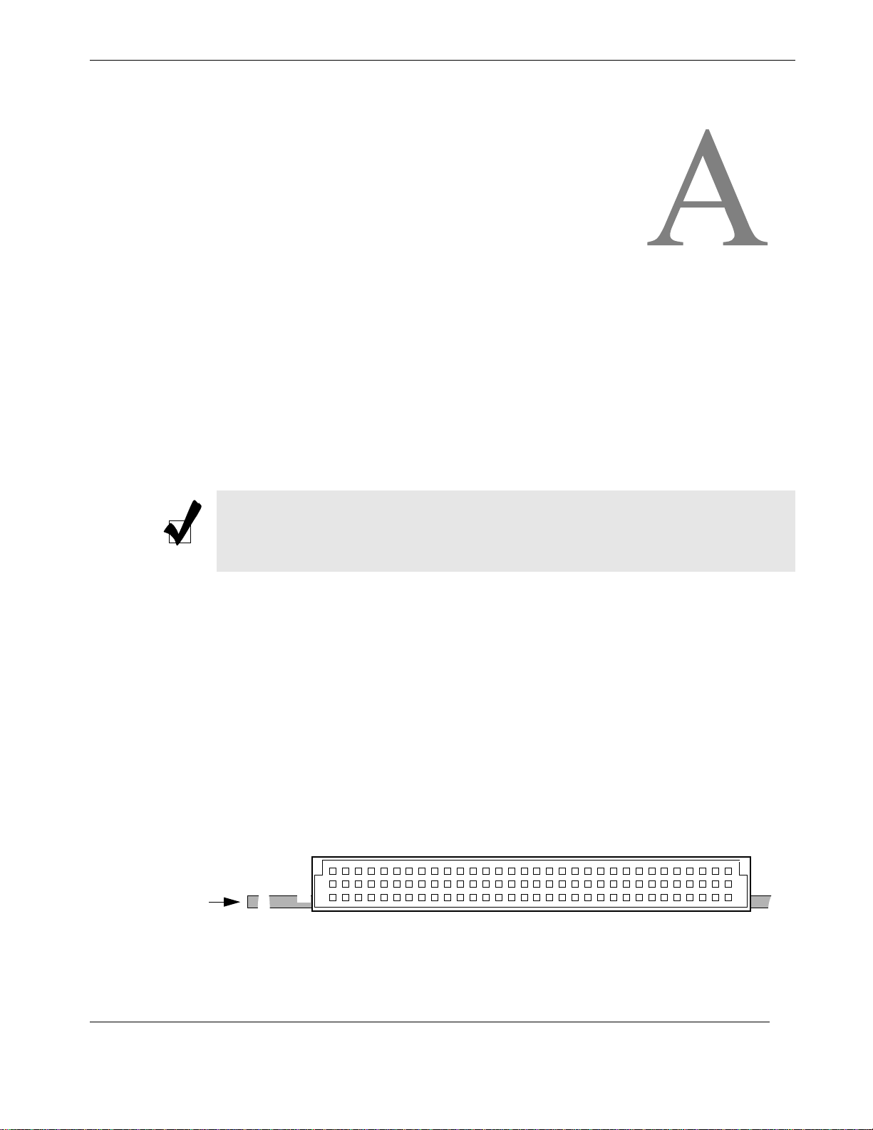
z Connector Type: 3-row, 96 pins (3x32), VME64 (Male)
z Manufacturer; Part Number: Harting; 9031966921
The connector pinout for the 3-row, VME P1 connector is shown in Figure A-1.
Connector-pin signal descriptions are described in Table A-1 on page A-2.
32
Row C
B
Bottom Edge of Board
Themis Computer
A
Figure A-1. XV1 VME P1 Connector Pinout
P1
1
A-1

XV1 Hardware Manual
Table A-1. XV1 VME P1 Connector-Pin Signals
Pin Row A Signal Row B Signal Row C Signal
1 VME_D00 VME_BBSY_L VME_D08
2 VME_D01 VME_BCLR_L VME_D09
3 VME_D02 VME_ACFAIL_L VME_D10
4 VME_D03 VME_BGIN0_L VME_D11
5 VME_D04 VME_BGOUT0_L VME_D12
6 VME_D05 VME_BGIN1_L VME_D13
7 VME_D06 VME_BGOUT1_L VME_D14
8 VME_D07 VME_BGIN2_L VME_D15
9 GND VME_BGOUT2_L GND
10 VME_SYSCLK VME_BGIN3_L VME_SYSFAIL_L
11 GND VME_BGOUT3_L VME_BERR_L
12 VME_DS1_L VME_BR0_L VME_SYSRESET_L
13 VME_DS0_L VME_BR1_L VME_WORD_L
14 VME_WRITE_L VME_BR2_L VME_AM5
15 GND VME_BR3_L VME_A23
16 VME_DTACK_L VME_AM0 VME_A22
17 GND VME_AM1 VME_A21
18 VME_AS_L VME_AM2 VME_A20
19 GND VME_AM3 VME_A19
20 VME_IACK_L GND VME_A18
21 VME_IACKIN_L Not Connected VME_A17
22 VME_IACKOUT_L Not Connected VME_A16
23 VME_AM4 GND VME_A15
24 VME_A07 VME_IRQ7_L VME_A14
25 VME_A06 VME_IRQ6_L VME_A13
26 VME_A05 VME_IRQ5_L VME_A12
27 VME_A04 VME_IRQ4_L VME_A11
28 VME_A03 VME_IRQ3_L VME_A10
29 VME_A02 VME_IRQ2_L VME_A09
30 VME_A01 VME_IRQ1_L VME_A08
31 –12V Not Connected +12V
A-2
32 VCC VCC VCC
_L Indicates an active low.
Themis Computer

A.1.2 VME P2 Connector
z Connector Type: 5-row, 160 pins (5x32), VME64 (Male)
z Manufacturer; Part Number: Harting; 02-01-160-2101
The connector pinout for the 5-row XV1 VME P2 connector is shown in Figure A-2.
Connector-pin signals routed to the P2 connector are described in Table A-2 on page
A-4. To access these P2 connector signals, a XV1 VME P2 Paddle Board (purchased
separately) must be attached to the P2 backplane behind the XV1 (refer to Section
A.5, “XV1 P2 Paddle Board,” on page A-12).
A—Connector Pinouts and Signal Descriptions
XV1 Rear Connectors
Bottom Edge of Board
Row D
32
C
B
A
Row Z
P2
1
Figure A-2. XV1 VME P2 Connector Pinout
VME P2-connector pinouts signal assignments vary with the board jumper-resistor
configurations (refer to Appendix B, “Jumper Pins and Solder Beads” for details).
Note: In Table A-2,
•an _L indicates an active low
• (–) and (+) indicate one member of a signal pair
•a thick border groups associated signals
Themis Computer
A-3

XV1 Hardware Manual
Table A-2. XV1 VME P2 Connector-Pin Signals
Pin Row Z Signal Row A Signal Row B Signal Row C Signal Row D Signal
1 VGA2_RED PWR_EN_L VCC (+5V) USB4P GND
2 GND VIN_AUX GND USB4N LAN_B_MDIN0
3 VGA2_GREEN VIN_AUX VME_RETRY_L USB5P LAN_B_MDIP0
4 GND GND VME_A[24] USB5N GND
5 VGA2_BLUE VIN_AUX VME_A[25] OC_USB4_P2_L LAN_B_MDIN1
6 GND GND VME_A[26] OC_USB5_P2_L LAN_B_MDIP1
7 HSYNC2 VIN_AUX VME_A[27] OC_USB2_P2_L GND
8 GND GND VME_A[28] OC_USB3_P2_L LAN_B_MDIN2
9 VSYNC2 SATA_TXP3B VME_A[29] SIO_TXD2_P2 LAN_B_MDIP2
10 GND SATA_TXN3B VME_A[30] SIO_RXD2_P2 GND
11 VGA2_DDC_DAT SATA_RXP3B VME_A[31] PS2_KB_CLK_P2 LAN_B_MDIN3
12 GND SATA_RXN3B GND PS2_KB_DATA_P2 LAN_B_MDIP3
13 VGA2_DDC_CLK GND VCC (+5V) PS2_MS_CLK_P2 GND
14 GND SATA_TXP4 VME_D[16] PS2_MS_DATA_P2 LAN_A_MDIN0
15 VCC SATA_TXN4 VME_D[17] SIO_SMBDATA_B LAN_A_MDIP0
16 GND SATA_RXP4 VME_D[18] SIO_SMBCLK_B GNC
17 V_3V3 SATA_RXN4 VME_D[19] HDA_RST_L LAN_A_MDIN1
18 GND GND VME_D[20] HDA_SYNC LAN_A_MDIP1
19 V_1V8 SATA_TXP5 VME_D[21] HDA_BIT_CLK GND
20 GND SATA_TXN5 VME_D[22] HDA_SDIN3 L AN_A_MDIN2
21 SIO_RTS1_P2_L SATA_RXP5 VME_D[23] HDA_SDOUT LAN_A_MDIP2
22 GND SATA_RXN5 GND USB2P GND
23 SIO_DTR1_P2_L GND VME_D[24] USB2N LAN_A_MDIN3
24 GND GND VME_D[25] USB3P LAN_A_MDIP3
25 SIO_CTS1_P2_L VIN_AUX VME_D[26] USB3N GND
26 GND GND VME_D[27] SIO_TXD1_P2 V_1V8
27 SIO_DSR1_P2_L VIN_AUX VME_D[28] SIO_RXD1_P2 LAN_LINKB100_L
28 GND GND VME_D[29] VIN_AUX LAN_LINKB1000_L
29 SIO_DCD1_P2_L VIN_AUX VME_D[30] VIN_AUX LAN_ACTB_L
30 GND GND VME_D[31] V_3V3 LAN_LINKA100_L
31 SIO_RI1_P2_L VIN_AUX GND GND LAN_LINKA1000_L
32 GND VIN_AUX VCC (+5V) ALL_PWRGD LAN_ACTA_L
A-4
Themis Computer

A—Connector Pinouts and Signal Descriptions
A.2 XV1 Front-Panel Connectors
A.2.1 Gigabit Ethernet (GbE) Port C
z Connector Type: Single RJ45 GBE Connector, 8 Pin, 2 LEDs, transformer
z Manufacturer; Part Number: Pulse; J0G-0009NL
The XV1 provides a single Gigabit Ethernet (Ethernet C) port on its front panel. The
RJ45 (8-pin) GBE connector contains two embedded LEDs, supports 10/100/
1000Base-T transmission (see Figure A-3 and Table A-3 below), and has an embed-
ded transformer for signal conversion.
Symbol
XV1 Front-Panel Connectors
Pin 8
Pin 1
Baseboard
Link Speed LED
Network Traffic LED
Figure A-3. Gigabit Ethernet RJ45 Connector Pinout
Table A-3. Gigabit Ethernet Connector-Pin Signals and LED Interpretation
Pin Signal Description LED LED Color Interpretation
1 BI_DA+ Bi-directional pair A+
2 BI_DA– Bi-directional pair A–
3 BI_DB+ Bi-directional pair B+ Yellow 100 Mb/s
4 BI_DC+ Bi-directional pair C+ Green 1000 Mb/s
5 BI_DC– Bi-directional pair C–
6 BI_DB– Bi-directional pair B–
7 BI_DD+ Bi-directional pair D+
8 BI_DD– Bi-directional pair D–
Yellow/
Green
(Top)
= Link
Speed
Green
(Bottom)
= Network
Traffic
OFF 10 Mb/s
Flashing rate is 300 ms for
transmit/receive activity.
Themis Computer
A-5

XV1 Hardware Manual
A.2.2 Multiple-I/O Connector
z Connector Type: 4-row, 60-pin (4x15) D-shell connector (Female)
z Manufacturer; Part Number: Molex; 70928-2003
The XV1 provides a single 60-pin connector on its front panel that supports four
types of I/O ports; namely:
• Two Serial ports (COM1, COM2)
• One SATA port (SATA3)
• Two USB 2.0 ports (USB0, USB1)
• One VGA graphics port
To connect with each of these ports, a special multi-split connector cable is provided
that can be attached directly to the multiple-I/O port (see Figure A-4).
SATA 3
USB0 / USB1
COM1
COM2
VGA Graphics
Figure A-4. Multiple-I/O Connector Cable
A connector pinout for the multiple-I/O connector is shown in Figure A-5.
15
16
46 60
Baseboard
Figure A-5. Multiple-I/O Connector Pinout
1
30
3145
Attach to 60-pin
Multiple-I/O Port
on XV1 faceplate
A-6
Themis Computer

A—Connector Pinouts and Signal Descriptions
XV1 Front-Panel Connectors
Connector-pin signals for the multiple-I/O connector are described in Table A-4.
Table A-4. Multiple-I/O Connector-Pin Signals
Pin Signal Pin Signal Pin Signal Pin Signal
1 USB2N FP 30 5V USB1 FP 31 HSYNC_5V 60 VSYNC_5V
2 USB2P FP 29 GND 32 VGA_DDC_DAT_5V 59 VGA_DDC_CLK_5V
3 USB1N FP 28 5V USB0 FP 33 VGA1_RED_OUT 58 GND
4 USB1P FP 27 GND 34 VGA1_GREEN_OUT 57 GND
5GND 26Unconnected 35 VGA1_BLUE_OUT 56 GND
6 SATA_RXP3 25 Unconnected 36 GND 55 5V_VGA_CONN
7SATA_RXN324Unconnected 37 GND 54 GND
8GND 23Unconnected 38 SIO_DTR1_FP_L 53 SIO_RI1_FP_L
9 SATA_TXN3 22 SIO_TXD2_FP 39 SIO_TXD1_FP 52 SIO_CTS1_FP_L
10 SATA_TXP3 21 SIO_RXD2_FP 40 SIO_RXD1_FP 51 SIO_RTS1_FP_L
11 GND 20 GND 41 SIO_DCD1_FP_L 50 SIO_DSR1_FP_L
12 Unconnected 19 Unconnected 42 Unconnected 49 Unconnected
13 Unconnected 18 Unconnected 43 Unconnected 48 Unconnected
14 Unconnected 17 Unconnected 44 Unconnected 47 Unconnected
15 Unconnected 16 Unconnected 45 Unconnected 46 Unconnected
A.2.2.1 Serial Ports COM1 & COM2
As shown in Table A-4, serial port COM1 is supported by multiple-I/O connector
pins 38 to 41 and 50 to 53 (these include signals for modem support).
Serial port COM2 is supported by multiple-I/O connector pins 21 and 22 (transmit
and receive only).
A.2.2.2 SATA3 Port
Themis Computer
The SATA3 port is supported by multiple-I/O connector pins 6, 7, 9, and 10 (see
Table A-4).
A-7

XV1 Hardware Manual
1
2
63
64
A.2.2.3 USB Ports USB0 & USB1
USB ports USB0 and USB1 are supported by multiple-I/O connector pins 1 to 4 and
pins 28 and 30 (see Table A-4).
A.2.2.4 VGA Graphics Port
The VGA graphics port is supported by multiple-I/O connector pins 31 through 35
and pins 55, 59, and 60 (see Table A-4).
A.3 Push-Button RESET
A recessed push-button RESET switch is located behind the Front Panel of the XV1
and is accessible by inserting an object the size of a paper clip. The RESET switch
will initiate a POR Reset, which is propagated throughout the XV1.
A.4 XV1 PMC Module Card Connectors
z Connector Type: 2-row, 64-pin connector (Female) (4 required)
z Manufacturer; Part: Molex; 71439-0864
An optional PMC Module card can be connected to the top side of the XV1 through
four 64-pin connectors (the interface VIO supports 3.3V @66 MHz only):
• J21 / J11..............................................................................................32-bit PCI
• J22 / J12 .............................................................................................32-bit PCI
•J23.......................................................................................................64-bit PCI
•J24.............................................................................................User I/O defined
The PMC Module card has no I/O through the VME P2 connector of the XV1. The
connector used for PMC card installation is shown in Figure A-6; three connectors
are required for 64-bit operation, and two connectors for 32-bit operation.
J11, J12, J21, J22, J23, J24
A-8
Figure A-6. PMC Module Card Connector (4 required)
Themis Computer
A—Connector Pinouts and Signal Descriptions
A.4.1 PMC Module Connector J21 / J11
PMC signals (32-bit PCI) for connectors J21 and J11 are described in Table A-5.
XV1 PMC Module Card Connectors
Table A-5. PMC Module Card Connector J21/J11
Pin (J3401) Signal Pin (J3401) Signal
1TCK 2-12V
3Ground 4INTA#
5INTB# 6INTC#
7 BUSMODE1# 8 +5V
9 INTD# 10 PCI-RSVD
11 Ground 12 PCI-RSVD
13 CLK 14 Ground
15 Ground 16 GNT#
17 REQ# 18 +5V
19 +3.3V 20 AD[31]
21 AD[28] 22 AD[27]
23 AD[25] 24 Ground
25 Ground 26 C/BE[3]#
27 AD[22] 28 AD[21]
29 AD[19] 30 +5V
31 +3.3V 32 AD[17]
33 FRAME# 34 Ground
35 Ground 36 IRDY#
37 DEVSEL# 38 +5V
39 Ground 40 LOCK#
41 SDONE# 42 SBO#
43 PAR 44 Ground
45 V(I/0) 46 AD[15]
47 AD[12] 48 AD[11]
49 AD[09] 50 +5V
51 Ground 52 C/BE[0]#
53 AD[06] 54 AD[05]
55 AD[04] 56 Ground
57 +3.3V 58 AD[03]
59 AD[02] 60 AD[01]
61 AD[0] 62 +5V
63 Ground 64 REQ64#
a
Signals (32 bit)
Themis Computer
a—Connectors J21/J11 corresponds to the PMC standard Jn1.
A-9

XV1 Hardware Manual
A.4.2 PMC Module Connector J22 / J12
PMC signals (32-bit PCI) for connectors J22 and J12 are described in Table A-6.
Table A-6. PMC Module Card Connector J22/J12
Pin (J3402) Signal Pin (J3402) Signal
1+12V 2TRST#
3TMS 4TDO
5TDI 6Ground
7Ground 8PCI-RSVD
9 N/C 10 PCI-RSVD
11 BUSMODE2# 12 +3.3V
13 RST# 14 BUSMODE3#
15 +3.3V 16 BUSMODE4#
17 PCI-RSVD 18 Ground
19 AD[30] 20 AD[29]
21 Ground 22 AD[26]
23 AD[24] 24 +3.3V
25 IDSEL 26 AD[23]
27 +3.3V 28 AD[20]
29 AD[18] 30 Ground
31 AD[16] 32 C/BE[2]#
33 Ground 34 PMC-RSVD
35 TRDY# 36 +3.3V
37 Ground 38 STOP#
39 PERR# 40 Ground
41 +3.3V 42 SERR#
43 C/BE[1]# 44 Ground
45 AD[14] 46 AD[13]
47 Ground 48 AD[10]
49 AD[08] 50 +3.3V
51 AD[07] 52 PMC-RSVD
53 +3.3V 54 PMC-RSVD
55 PMC-RSVD 56 Ground
57 PMC-RSVD 58 PMC-RSVD
59 Ground 60 PMC-RSVD
61 ACK64# 62 +3.3V
63 Ground 64 PMC-RSVD
a
Signals (32 bit)
A-10
a—Connector J7 corresponds to the PMC standard Jn2.
Themis Computer

A.4.3 PMC Module Connector J23
PMC signals (64-bit PCI) for connector J23 are described in Table A-7.
A—Connector Pinouts and Signal Descriptions
XV1 PMC Module Card Connectors
Table A-7. PMC Module Card Connector J23
Pin (J3403) Signal Pin (J3403) Signal
1PCI-RSVD 2Ground
3 Ground 4 C/BE[7]#
5 C/BE[6]# 6 C/BE[5]#
7 C/BE[4]# 8 Ground
9 +3.3V 10 PAR64
11 AD[63] 12 AD[62]
13 AD[61] 14 Ground
15 Ground 16 AD[60]
17 AD[59] 18 AD[58]
19 AD[57] 20 Ground
21 +3.3V 22 AD[56]
23 AD[55] 24 AD[54]
25 AD[53] 26 Ground
27 Ground 28 AD[52]
29 AD[51] 30 AD[50]
31 AD[49] 32 Ground
33 Ground 34 AD[48]
35 AD[47] 36 AD[46]
37 AD[45] 38 Ground
39 +3.3V 40 AD[44]
41 AD[43] 42 AD[42]
43 AD[41] 44 Ground
45 Ground 46 AD[40]
47 AD[39] 48 AD[38]
49 AD[37] 50 Ground
51 Ground 52 AD[36]
53 AD[35] 54 AD[34]
55 AD[33] 56 Ground
57 +3.3V 58 AD[32]
59 PCI-RSVD 60 PCI-RSVD
61 PCI-RSVD 62 Ground
63 Ground 64 PCI-RSVD
a
Signals (64 bit)
Themis Computer
a—Connector J23 corresponds to the PMC standard Jn3.
A-11

XV1 Hardware Manual
A.4.4 PMC Module Connector J24
PMC connector J24 (which is not installed on the standard XV1 configuration), supports
user-defined I/O signals that to support specific functions (a floppy drive, for example).
Call Themis Customer Support for a detailed list of supported J24 signals.
A.5 XV1 P2 Paddle Board
Figure D-2 on page D-3 in Appendix D, ”Board Component and Connector Diagrams” shows XV1 P2 Paddle-Board I/O connectors, which are described in the following sections.
A.5.1 Serial COM1 and COM2 Connectors
z Connector Type: Dual micro-D, 9-pin (Male) each, Right Angle, 2 required
z Manufacturer; Part: ITT Cannon; MDSM-18PE-Z10-VR25
The XV1 VME P2 Paddle Board contains two serial ports (COM1 and COM2) on its
front edge, with COM1 offering modem support (see Figure A-7 for a connector
pinout, and Table A-8 on page A-13 for pinout descriptions). Note that modem sup-
port is available only through a 5-row VME backplane; a 3-row VME backplane
supports transmit and receive signals only (see Table A-2 on page A-4). With proper
modifications, COM1 and COM2 are also accessible from the XV1 front panel, in
which case, they cannot be accessed through the Paddle Board. Call the Themis sales
office at the time of purchase to inform them as to where you would like to access
the COM1 and COM2 ports.
Symbol
Important Note
A resistor adjustment must be made
before COM1 and COM2 can be
accessed from the P2 Paddle Board
(access denied from the Front Panel).
5
1
Serial Ports
COM1 COM2
9
6
J7
Paddle Board Edge
A-12
Figure A-7. P2 Paddle Board Serial COM1 and COM2 Connector Pinout
Themis Computer

A—Connector Pinouts and Signal Descriptions
2
1
3
5
8
6
4
7
XV1 P2 Paddle Board
Table A-8. P2 Paddle Board Serial COM1 and COM2 Connector-Pin Signals
Serial Port COM1 Serial Port COM2
Pin Signal Name Pin Signal Name Pin Signal Name Pin Signal Name
A1 SIO_DCD1_L A6 SIO_DSR1_L B1 GND B6 NC
A2 SIO_RXD1 A7 SIO_RTS1_L B2 SIO_RXD2 B7 NC
A3 SIO_TXD1 A8 SIO_CTS1_L B3 SIO_TXD2 B8 NC
A4 SIO_DTR1_L A9 SIO_RI1_L B4 NC B9 NC
A5 GND B5 NC
A.5.2 DIN-8 PS/2 Keyboard/Mouse Connector
z Connector Type: 8-pin mini-DIN (Female)
z Manufacturer; Part Number: TYCO/AMP; 749179-1
z Themis Cable P/N: 110104-002
Connector-pin signals for the 8-pin mini-DIN PS/2 port (see Figur e A-8) on the XV1
P2 Paddle Board are given in Table A-9.
Symbol
Note: NC = No Connect
J2
Paddle Board Edge
Figure A-8. P2 Paddle Board PS/2 Mini-DIN Connector Pinout
Table A-9. P2 Paddle Board PS/2 Connector-Pin Signals
Pin PS/2 Signal Pin PS/2 Signal
1 GND (Ground) 5 KBD_CLK
2 GND (Ground) 6 KBD_DATA
3 +5V (Fu sed, 1.3A max) 7 MOUSE_CLK
Themis Computer
4 MOUSE_DATA 8 +5V (Fused, 1.3A max)
A-13
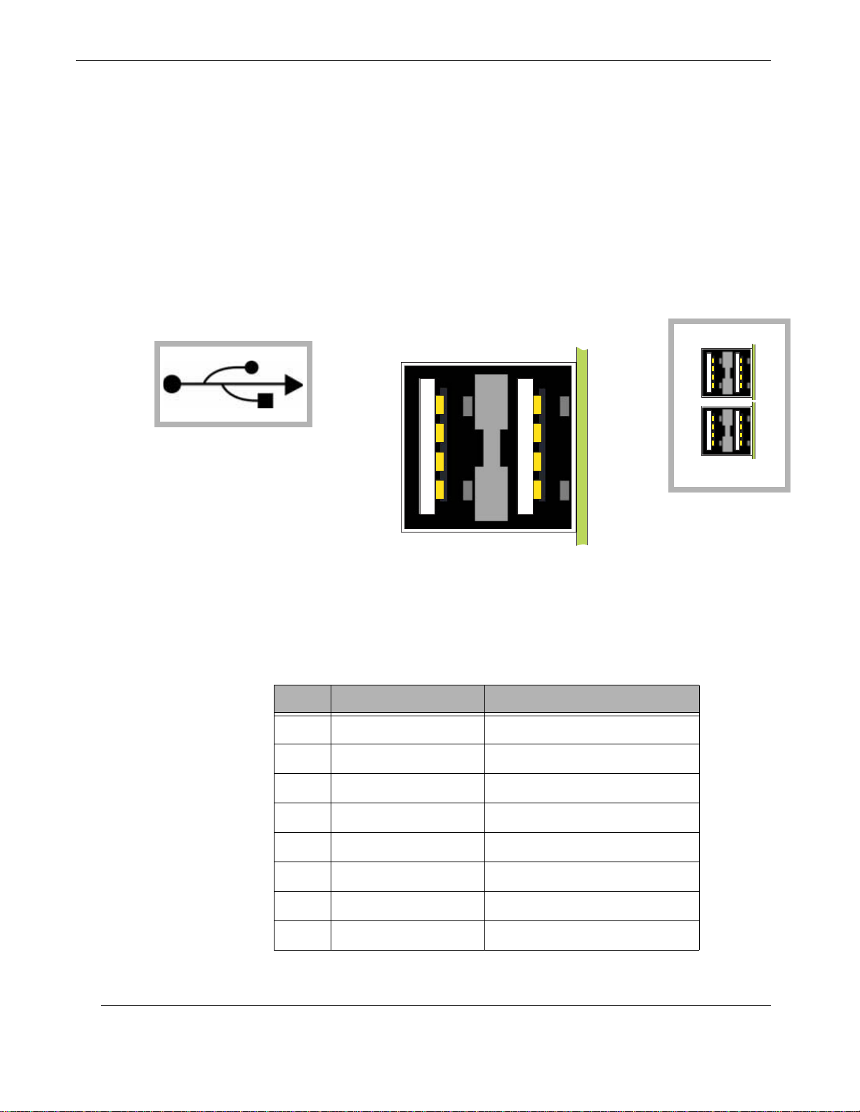
XV1 Hardware Manual
4
3
2
1
4
3
2
1
4
3
2
1
4
3
2
1
A.5.3 USB Ports USB2 / USB3 and USB4 / USB5
z Connector Type: Type A, Dual Stacked USB
z Manufacturer; Part: AMP; 5787617-4
The XV1 P2 Paddle Board supports four USB Ports: dual USB2 / USB3 and dual
USB4 / USB5, all installed on its front edge. A pinout for these stacked connectors is
given in Figure A-9, and connector-pin signals are described in Table A-10. All USB
ports support both version 2.0 and 1.1 standards.
Symbol
USB Ports
USB3 USB2
USB3/USB5 USB2/USB4
4
3
2
1
4
3
2
USB5 USB4
1
J3 / J6
Paddle Board Edge
Figure A-9. P2 Paddle Board Dual USB Ports 2/3 and 4/5 Connector Pinout
Table A-10. USB Ports 2/3 and 4/5 Connector-Pin Signals
Pin USB Signal Description
A1 USB0_PWR USB C Power
J3
J6
A2 USB0_D_N USB C Data - Negative
A3 USB0_D_P USB C Data - Positive
A4 USB0_GND USB C Ground
B1 USB1_PWR USB D Power
B2 USB1_D_N USB D Data - Negative
B3 USB1_D_P USB D Data - Positive
B4 USB1_GND USB D Ground
A-14
Themis Computer

A—Connector Pinouts and Signal Descriptions
5
1
10
6
15
11
XV1 P2 Paddle Board
A.5.4 SVGA Monitor Port (5-Row VME Backplane Only)
z Connector Type: 15-pin, D-Subminiature (Female) SVGA Connector
z Manufacturer; Part: AMP; 2-1734344-3
A Super-VGA connector is installed on the XV1 P2 Paddle Board on its front edge.
A pinout for this connector is given in Figure A-10, and connector-pin signals are
described in Table A-11. Note that the SVGA port is supported only from a 5-row
VME backplane.
The P2 Paddle Board video SVGA signals are a redundant image of those from the
XV1 Front Panel through the multiple-I/O connector.
Symbol
SVGA Display Port
J10
Paddle Board Edge
Figure A-10. P2 Paddle Board SVGA Connector Pinout
Table A-11. P2 Paddle Board SVGA Connector-Pin Signals
Pin VGA Signal Description Pin VGA Signal Description
1 RED OUT Red signal output 9 VCC Filtered Vcc voltage source
2 GREEN OUT Green signal output 10 GND Ground
3 BLUE OUT Blue signal output 11 NC No connection
4 NC No connection 12 SDA Display Data Channel—Data
5 GND Ground 13 HSYNC Horizontal synchronization
6 GND Ground 14 VSYNC Vertical synchronization
7 GND Ground 15 SCL Display Data Channel—Clock
Themis Computer
8 GND Ground
A-15

XV1 Hardware Manual
17
A.5.5 SATA Ports 3, 4, and 5
z Connector Type: Single 7-pin SATA Plug and Dual 7-pin SATA
z Manufacturer; Part: Molex; 47080-4005 (Single) / Circuit Assy; CA-D14SA
HPR-C-0-5T (Dual)
Three SATA (Serial ATA) connectors (SATA3, SATA4, SATA5) are installed on
the front edge of the XV1 CPU-0 P2 Paddle Board. A pinout is given in Figure A-11,
and connector-pin signals are described in Table A-12.
Symbol
Note: The SATA4 and SATA5
connectors are joined in
a dual assembly.
Figure A-11. P2 Paddle Board SATA Connector Pinout
Table A-12. P2 Paddle Board SATA Connector-Pin Signals
Pin VGA Signal Description
SATA3 Port
SATA4 Port
SATA5 Port
J4
17
17
J5
Paddle Board Edge
1 GND Ground
2 Tx A+ Transmit Signal A-Positive
3 Tx A– Transmit Signal A-Negative
4 GND Ground
5 Rx A+ Receive Signal A-Positive
6 Rx A– Receive Signal A-Negative
7 GND Ground
A-16
Themis Computer
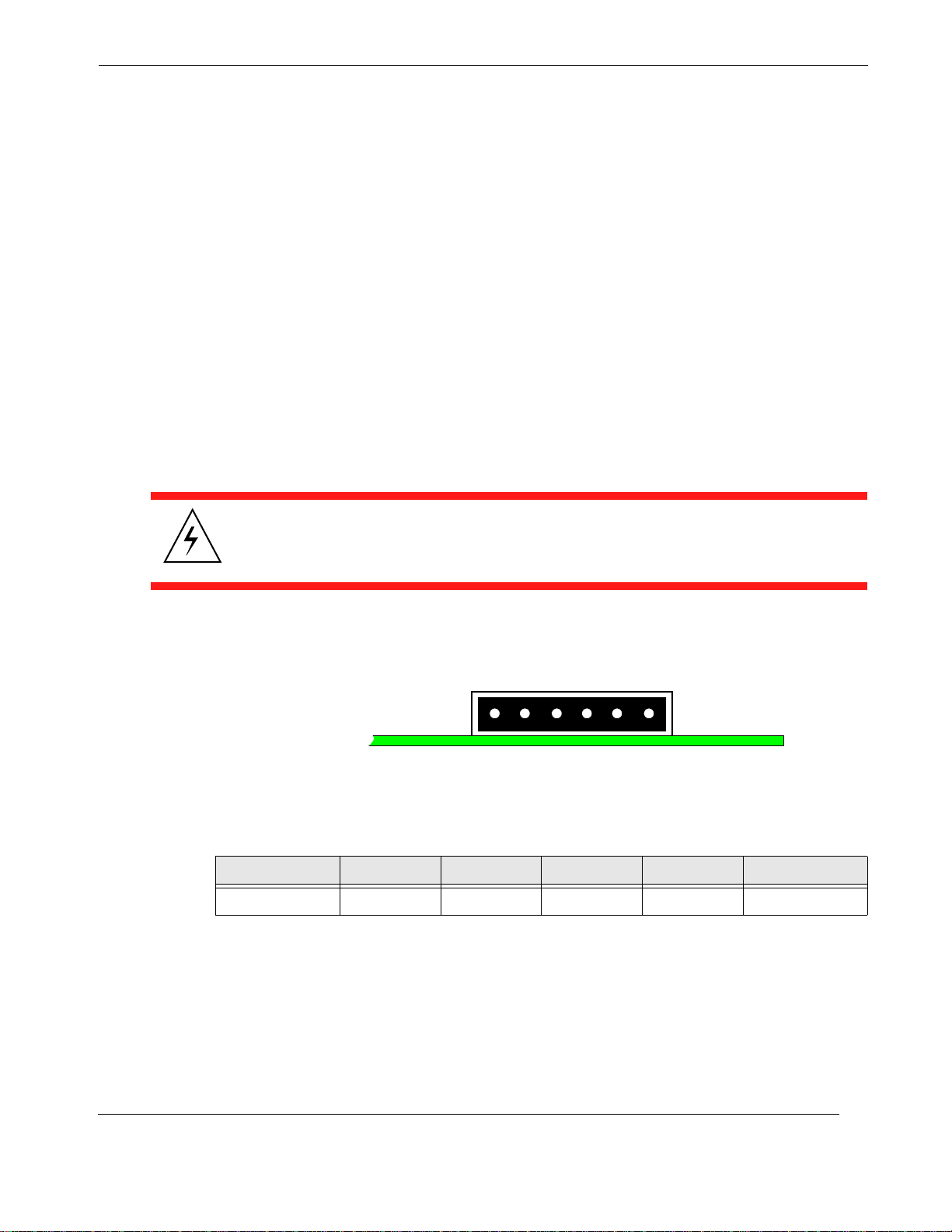
A—Connector Pinouts and Signal Descriptions
A.5.6 Auxiliary +12-Volt/+5-Volt Power Connectors
z Connector Type: 6-pin In-line Connector (Female), 2 required
z Manufacturer; Part: Molex; 43650-0600
z Themis Cable P/N: 111230-001
A.5.6.1 Auxiliary +12-Volt Power Connector
The XV1 P2 Paddle Board provides +12-volt power to the XV1 from the 12-volt rail
through multiple P2 pins in row A (see Table A-2 on page A-4) of the VME P2 backplane.
The system power supply also provides +12 volts to the paddle board through the 6-pin
Molex connector J1 or J15—only one +12-volt connection is required (see Figure A-12;
the mating plug is an ITT Cannon connector, P/N 192990-0980). Use power cable P/N
11 1230-001.
XV1 P2 Paddle Board
Warning: The Themis cable connected to this power connector should receive
+12V directly from the +12V lug on the chassis power supply , not from +12V pins
on the backplane or from the +12V cable supplying the backplane.
Power connector pinout signals are defined in Table A-13.
6
Paddle Board Edge
Figure A-12. P2 Paddle Board Power Connector Pinouts
Table A-13. +12V/+5V Power Connector-Pin Signals
Pin 1 Pin 2 Pin 3 Pin 4 Pin 5 Pin 6
+12V / +5V +12V / +5V +12V / +5V Ground Ground Ground
A.5.6.2 Auxiliary +5-Volt Power Connectors
1
J1 / J15
Themis Computer
The system power supply can also provide +5 volts to the paddle board through connectors
J1 and J15—both +5-volt connections are required. Use two power cables (P/N 111230-
001).
A-17

XV1 Hardware Manual
A.5.7 Stereo Audio In/Out Connectors
z Connector Type: Stereo Mini-Jack (3.5 mm), 2 required
z Manufacturer; Part: Kobicon; 161-3503-EX
The two stereo (L/R) audio connectors on the front edge of the P2 Paddle Board are
shown in Figure A-13, and are used to transmit HDA audio signals, one for input,
the other for output.
J14 J13
Paddle Board Front Edge
Figure A-13. P2 Paddle Board Stereo Audio Connectors
StereoStereo
In JackOut Jack
A.5.8 Gigabit Ethernet A and Ethernet B (5-Row VME
Backplane Only)
Both gigabit Ethernet A and Ethernet B on the P2 Paddle Board are used for Themis
testing purposes only.
A-18
Themis Computer

B
Appendix
Jumper Pins and Solder Beads
This appendix provides jumper-pin and solder-bead locations and configurations for the
XV1. Solder beads are considered “factory-configurable” and must not be altered by
the user . If a solder bead requires reconfiguration, contact Themis Customer Service.
Warning: Solder beads are set by Themis at the factory. Attempting to alter a solder-bead configuration could seriously damage the XV1. If you encounter a problem, contact Themis Customer Support.
DO NOT ATTEMPT TO ALTER SOLDER-BEAD CONFIGURATIONS.
B.1 Field-Configurable Jumper Pins
B.1.1 XV1 Jumper Pins
Jumper pins are found only on the top side of the XV1 system board and are
described in Table B-1 on page B-2. In Table B-1, an ON or Short jumper position
means the jumper is installed, shorting the pins and completing the circuit. OFF
means there is no jumper installed, hence the path between the pins is open, breaking
the circuit.
Figure B-1 on page B-3 shows the location of all jumpers on the XV1. In Figure
B-1, jumper pin 1 is identified with a square and a triangle.
Themis Computer
B-1
XV1 Hardware Manual
Table B-1. XV1 Jumper-Pin Settings (Top Side Only)
Jumper
Pins
JP1
JP2
JP3
JP4
JP5
JP6
JP7
Jumper
Position
a
ON Clears CMOS.
OFF Normal operation.
b
ON Enables boot from SPI
.
OFF Does not enable boot from SPI.
ON
Reserved for future use.
OFF
b
ON Selects Backup SPI
BIOS.
OFF Selects Primary SPI BIOS.
ON STEC flash is write-protected.
OFF STEC flash is not write-protected.
ON
For factory purposes only.
OFF
ON Disables onboard video.
OFF Enables onboard video.
Description
ON
VME System Controller is disabled.
Note: If SB7 (see Table B-3 on page B-6) is shorted, this function is reversed.
JP8
OFF
a—Boldface = the default jumper position. Absence of a default position indicates a manufacturing or user decision.
b—SPI = Serial Peripheral Interface.
TSI148 PCI-X-to-VME Bridge evaluates backplane signal BG3IN_ to determine
whether to enable the VME System Controller.
B.1.2 Memory Module Jumper Pins
There are no jumper pins on the XV1 Memory Modules.
B-2
Themis Computer
B—Jumper Pins and Solder Beads
Field-Configurable Jumper Pins
JP2 JP1 JP4 JP3 JP5 JP8 JP7 JP6
Legend
See Figure B-3 for
Solder-Bead Legend.
Jumper
OFF
Jumper
ON
Pin 1
SB6
VME P1
Top Side
VME P0
VME P2
Figure B-1. XV1 Jumper-Pin and Solder-Bead Locations (Top Side)
Themis Computer
B-3

XV1 Hardware Manual
B.1.3 XV1 Paddle-Board Jumper Pins
Jumper pins are found only on the top side of the XV1 Paddle Board and are
described in Table B-2.
In Table B-2, an ON jumper position means the jumper is installed, shorting the pins
and completing the circuit. OFF means there is no jumper installed, hence the path
between the pins is open, breaking the circuit.
Table B-2. XV1 Paddle-Board Jumper-Pin Settings (Top Side Only)
Jumper Pins
JP1, JP2
Jumper
Position
ON
OFF
Description
Manufacturing use only.
Figure B-2 on page B-5 shows the location of both jumpers on the XV1 Paddle
Board. In Figure B-2, jumper pin 1 is identified with a square and a triangle.
B.2 Factory-Configurable Solder Beads
B.2.1 XV1 Solder Beads
Solder beads are found mainly on the bottom side of the XV1 system board, with
one solder bead (SB6) located on the top side. All solder beads are described in
Table B-3 on page B-6.
In Table B-3, Short means a solder bead is installed, creating an electrical path
between two contacts. Open means no solder bead is installed, hence the path
between the contacts is open.
B-4
Figure B-3, page B-7, shows the location of all bottom-side solder beads on the
XV1. The location of the top-side SB6 is shown in Figure B-1 on page B-3.
Remember that pin 1 is indicated on the board by a thick bar line.
Caution: When dealing with a 3-pin solder-bead switch, a solder bead will short
only one set of pins, either 1–2 or 2–3.
If a solder bead shorts more than 2 pins, call Themis Customer Support.
Themis Computer

Legend
JP1
B—Jumper Pins and Solder Beads
Factory-Configurable Solder Beads
Jumper
OFF
Jumper
ON
Pin 1
JP2
Themis Computer
VME P2
Figure B-2. XV1 Paddle-Board Jumper-Pin Locations (Top Side)
B-5
XV1 Hardware Manual
Table B-3. XV1 Solder-Bead Settings (Bottom and Top Side)
Solder
Bead
SB1
SB2
SB3
SB4
SB5
SB6
[Top Side]
SB7
Setting
a
Description
Short Disable ES1000 VGA.
Open Enable ES1000 VGA.
Short 1–2 Compact Flash voltage is 5 volts.
Short 2–3 Compact Flash voltage is 3 volts.
Short 1–2
See Table B-4.
Short 2–3
Short 1–2
See Table B-4.
Short 2–3
Short 1–2
See Table B-4.
Short 2–3
Short Disable FPGA. [See Figure B-1, page B-3, for top-side location.]
Open Enable FPGA. [See Figure B-1, page B-3, for top-side location.]
Short
Defines function of jumper-pin JP8 (see Table B-1, page B-2).
Open
B-6
Short Enable Rx VME reset.
SB10
Open Disable Rx VME reset.
Short Enable Tx VME reset.
SB11
Open Disable Tx VME reset.
a—Boldface = the default solder-bead setting. Absence of a default setting indicates a manufacturing or user deci-
sion.
Table B-4. FSB Frequency Selection
SB5 [BSEL2] SB4 [BSEL1] SB3 [BSEL0] Frequency
Short 2–3 Open Open 166 MHz
Short 2–3 Open Short 2–3 200 MHz
Short 2–3 Short 2–3 Short 2–3 266 MHz
Open Short 2–3 Short 2–3 333 MHz
Short 1–2 Short 1–2 Short 1–2 CPU Select
Themis Computer

VME P1
B—Jumper Pins and Solder Beads
Factory-Configurable Solder Beads
SB7
SB10
SB11
SB1
VME P0
VME P2
SB2
Legend
Thick bar = Pin 1
Solder short,
pins 2 & 3
= Actual location
of solder beads
= Description
of solder beads
SB3 SB4 SB5
Bottom Side
Themis Computer
Note: Solder-bead SB6 is located on the
Top Side of the board (see Figure B-1).
Figure B-3. XV1 Solder-Bead Locations (Bottom Side)
B-7

XV1 Hardware Manual
B.2.2 Memory Module Solder Beads
There are no solder beads on the XV1 Memory Module.
B.2.3 XV1 Paddle-Board Solder Beads
There are no solder beads on the XV1 Paddle Board.
B-8
Themis Computer

C
Front-Panel I/O Connections and LEDs
C.1 Introduction
This appendix contains diagrams of all front panels (faceplates) for each possible
model configuration of the XV1. It is intended as a reference to I/O and monitoring
functions. See Table C-1 for a list of XV1 models.
Appendix
Caution: The PCI address of a PMC Module is not necessarily the same as the
PMC Module slot number.
Table C-1. XV1 Model Configurations
Model
XV1 / 1 1 Module (1 VME Slot)
XV1 / 2 2 Modules (2 VME Slots)
XV1 / 3 3 Modules (2 VME Slots)
C.1.1 Front-Panel Dimensions
A single-slot XV1 front panel measures 235-mm (9.25”) high by 20-mm
(0.78”) wide (with VME64-type handles) or 241-mm (9.5”) high by 20-mm
(0.78”) wide (with older Legacy-VME handles).
Baseboard
PMC/XMC Modules
Themis Computer
C-1

XV1 Hardware Manual
C.1.2 Injector/Ejector Handles
The XV1 is equipped with two types of injector/ejector handles (see Figure C-1 on
page C-3):
• VME64-type handles (Elma, for example), which aid in both the insertion and
the extraction of the PC board into and out of the VME backplane connectors
• Legacy-VME handles, which aid only in the extraction of the PC board from
the VME backplane connectors
When a PCB board product such as the XV1 is shipped from Themis, VME64-type
handles will be installed unless the customer specifies a different handle such as the
Legacy-VME.
C.1.2.1 VME64-type Handles
When ordered, all Themis board products are shipped with VME64-type handles
unless otherwise specified. A multiple-slot system will be shipped with all handles
secured together by mating pins. One pin is inserted through two adjacent handles.
This assures that all boards will lock onto and release from the VME rack frame at
the same time.
On those occasions when the customer is upgrading and must add or replace a board
in the system, it is important to make sure that a mating pin is used to secure two
adjacent handles.
C.1.2.2 Legacy-VME Handles
When extracting a multiple-board system from the VME rack frame, it is important
to remember that—since there is no mating pin to hold handles together—each handle works independently from all other handles, hence the operator must extract the
system from the rack frame by carefully manipulating each handle in the same direction until the system is totally removed from the rack.
Caution: Removal of the EMI shield and insertion of a spine between mating front
panels is a factory procedure and not recommended in the field.
C-2
Themis Computer

A VME64 Injector/Ejector Handle B Legacy-VME Ejector Handle
Figure C-1. PMC/XMC Injector/Ejector Handles
C.2 XV1 Front Panels
C—Front-Panel I/O Connections and LEDs
XV1 Front Panels
This section contains descriptive graphics of the front-panel I/O connections for
each XV1 model configuration listed in Table C-1 on page C-1 (see Figure C-3,
page C-4, through Figure C-5, page C-6).
C.2.1 Multiple-I/O Connector
The multiple-I/O connector on the XV1 front panel supports a total of four different
types of I/O ports (see Figure C-3)—dual serial (COM1/COM2), single SATA3,
dual 2.0 USB0/USB1, and VGA graphics. To attach to each of these different ports,
a special multi-split connector cable must be connected to the multiple-I/O connector (see Figure C-2).
SATA 3
USB0 / USB1
Attach to 60-pin
Multiple-I/O Port
on XV1 faceplate
Themis Computer
COM1
COM2
VGA Graphics
Figure C-2. Multiple-I/O Connector Cable
C-3

XV1 Hardware Manual
C.2.2 XV1/1—1 PMC/XMC Module
P
M
C
/
X
M
C
PMC/XMC Module
C-4
Gigabit Ethernet Port C (RJ45)
Status LEDs (2)
See Section C.3, “LEDs”, for interpretations
Multiple-I/O Port *
XV1
Baseboard
* Supported by multi-split connector cable.
Figure C-3. XV1/1 Front Panel
Serial COM1/COM2
Dual 2.0 USB 0/1 [KB/M]
SATA3 (SATA II)
VGA Graphics
Themis Computer

C.2.3 XV1/2—2 PMC/XMC Modules
P
M
C
/
PMC/XMC Module
X
M
C
C—Front-Panel I/O Connections and LEDs
XV1 Front Panels
PMC/XMC Module
See Figure C-3 for a description
of Front-Panel connectors
Baseboard
XV1
P
M
C
/
X
M
C
Themis Computer
Figure C-4. XV1/2 Front Panel
C-5

XV1 Hardware Manual
C.2.4 XV1/3—3 PMC/XMC Modules
PMC/XMC ModulePMC/XMC Module
P
M
C
/
X
M
C
P
M
C
/
X
M
C
PMC/XMC Module
P
M
C
/
X
M
C
C-6
See Figure C-3 for a description
of Front-Panel connectors
XV1
Baseboard
Figure C-5. XV1/3 Front Panel
Themis Computer

C.3 LEDs
Callouts indicating front-panel LEDs are shown in Figure C-6. Description and
interpretation of front-panel LEDs are given in Table C-2 on page C-8.
C—Front-Panel I/O Connections and LEDs
LEDs
A
C
D
B
XV1
Themis Computer
Figure C-6. XV1 Front-Panel LEDs
C-7

XV1 Hardware Manual
Table C-2. Front-Panel LED Interpretation
Item Callout
a
Function Color Frequency and/or Interpretation
Left LED A Drive Activity Yellow
Right LED B System Status Green
Off 10 Mbit/s
C Link Speed
Green 100 Mbit/s
Gigabit
Ethernet Port C
a—From Figure C-6 on page C-7.
D
Network
Activity
Amber 1000 Mbit/s
Green
This LED indicates drive activity for either
a SATA drive or the Compact Flash.
When the BIOS is POSTing, this LED
flashes at a 1-hertz rate.
This LED indicates system status. It flashes at a 1-hertz rate as the board goes
through BIOS POST. When the POSTing
is completed, it turns solid green.
If any power rail fails, the LED will not light
either during POST or afterwards.
LED lights when traffic is dete cted on the
network
C-8
Themis Computer

D
Appendix
Board Component and Connector Diagrams
The following sections of this appendix contain diagrams of the various boards of
the XV1. It is intended as a quick reference to component and connector identification. XV1 boards included are:
• Baseboard
• P2 Paddle Board
D.1 XV1 Baseboard
Figure D-1 on page D-2 identifies front-panel, major board-surface components, and
connectors as seen from the top side of the XV1 Baseboard.
D.2 P2 Paddle Board
Figure D-2 on page D-3 identifies the major connectors on the P2 Paddle Board, as
viewed from the top side.
Themis Computer
D-1

XV1 Hardware Manual
PMC/XMC
Module
Outline
Memory
Module
Outline
PMC/XMC
Module
Outline
Compact Flash Card Holder
Intel
ICH9R
I/O Controller
Hub (ICH)
NH82801IR
AT I
2D
Graphics
Lithium Coin Cell (3V)
Tsi148
PCI/X-to-VME
Bus Bridge
Tundra
TSI148-133CLY
SMSC
Super
I/O
VME P1
3.3V PMC
Lockout Key
VME P0
3.3V PMC
Lockout Key
Module
Module
Gigabit Ethernet C
Reset Switch
(bottom side)
Multiple-I/O Port
Top Side
D-2
Intel
5100
Memory Controller
Hub (MCH)
QG5100MCH
Intel
Quad-Core
L5408
Xeon Processor
2.13 GHz
Figure D-1. XV1 Component and Connector Diagram (Top Side)
VME P2
Heatsink
Outline
Themis Computer

On-Board
Audio Access
Connectors
D—Board Component and Connector Diagrams
P2 Paddle Board
I2C Connector
Line In
Stereo
Audio
Line Out
PS/2 Keyboard/Mouse
(Mini-DIN8)
Serial COM1 / COM2 (left)
(Dual 9-Pin D-Shell)
(Testing only)
VME P2
To VME 5-Row
or 3-Row
P2 Connector
SVGA Connector
(15 Pin D-Shell)
[
5-Row P2 Connector only
Dual USB2 / USB3
Dual USB4 / USB5
Gigabit Ethernet A
[
5-Row P2 Connector only
Gigabit Ethernet B
[
5-Row P2 Connector only
S ATA3
SATA4 / SATA5
]
]
Testing
only
]
Themis Computer
Figure D-2. Paddle Board Component and Connector Diagram (Top Side)
D-3

XV1 Hardware Manual
Caution: Connect the Paddle Board to the P2 connector of the VME B ackplane
only . Connection to the P1 connector will cause operational malfunctions as well as
possible damage to both the Baseboard and the Paddle Board.
D-4
Themis Computer

E
Appendix
VME Slot Configurations
The following 11” x 17” foldout (see Figur e E-1 on page E-3) illustrates the slot configura-
tions of all models of the XV1. Users may supplement the onboard XV1 graphics capability by installing a TGA-7000 PMC graphics accelerator card in an available PMC Module
slot.
Table E-1 summarizes all model configurations.
Table E-1. XV1 Model Configurations
Model
XV1 / 1 1 Module (1 VME Slot)
XV1 / 2 2 Modules (2 VME Slots)
XV1 / 3 3 Modules (2 VME Slots)
Baseboard
PMC/XMC Modules
Caution: The original Themis 2P2 PMC/XMC Ca rrier Board or 2P2/2P3 PMC
Carrier Boards physically cannot be installed onto the XV1. A new PMC/XMC
Carrier Board is presently being designed, but has not yet been released.
Themis Computer
E-1

XV1 Hardware Manual
E-2
Themis Computer

E
P
M
C
/
X
M
C
P
M
C
/
X
M
C
XV1
P
M
C
/
X
M
C
P
M
C
/
X
M
C
P
M
C
/
X
M
C
XV1
.
E–VME Slot Configurations
XV1
Model XV1 / 1
A
Top View
Model XV1 / 2
B
Top View
Model XV1 / 3
C
Baseboard
Baseboard
I/O Expansion Board
Front Panel
1 PMC Slot
0
2 PMC Slots
2 PMC Slots
VME Slots
PMC Sites
Audio I/O
1
1
0
XV1 / 1
VME Slots
PMC Sites
Audio I/O
2
2
0
VME Slots
PMC Sites
Audio I/O
XV1 / 2
P
M
C
/
X
M
C
2
3
0
XV1 / 3
Baseboard
Top View
1 PMC Slot
Note: The I/O Expansion Board is only 2/3 high (4RU).
= Single-height heat sink.
*
Approved PMC Cards
supported by Themis:
1
2
3
4
5/2009
5
= Double-height heat sink.
XV1
1VME Slot:
A
1
2
B
12
C
Themis Computer
Figure E-1. XV1 VME Slot Configurations
E-3

XV1 Hardware Manual
E-4
Themis Computer

Index
Symbols
+12-Volt Power Connector 1-7
+12-Volt/+5-Volt Power Connectors A-17
+5-Volt Power Connector 1-7
Numerics
10/100/1000Base-T Ethernet 1-5, A-5
5100 Memory Controller Hub 3-2
82571EB Dual Gigabit Ethernet Controller 3-3
82801 I/O Controller Hub (ICH) 3-2
A
AMP 2-1734344-3 A-15
AMP 5787617-4 A-14
AMP 749179-1 A-13
ATI ES1000 2D graphics accelerator 2-4
Auxiliary Functions 2-8
B
Baseboard 2-1, D-1
VME P1 Pinout A-2
VME P2 Connector A-3
VME P2 Connector Pinout A-4
Battery Replacement 1-8
BIOS 3-4
BIOS Flash 3-4
Block Diagram, XV1 2-2
Board Type 1-1
SATA3, SATA4, SATA5 1-7
Stereo Audio Connector 1-7
SVGA Video Port 1-6
USB2, USB3, USB4, USB5 1-6
Power 1-4
Serial, RS232, Micro DB9 to DB9 1-4
Carrier Boards 2-5, 3-5
Cautions xviii
Check Configurations 1-2
Comments are Welcome xix
Component and Connector Diagrams
Paddle Board 1-3, D-3
XV1 D-2
Customer Comments xiv
D
Daisy Chain Jumper Settings 1-8
Dimensions, Front Panel C-1
Dual Gigabit Ethernet Controller
Features 3-3
E
Environmental Specifications 2-9
Ethernet 3-3
Connector Pin Signals and LEDs A-5
Connector Pinout A-5
Ethernet C, Gigabit 1-5, 2-3
Ethernet Port C A-5
C
Cables
attaching 1-4, 1-5
Multiple-I/O Connector (60 pins) 1-4
Paddle Board 1-6
COM1 and COM2 1-6
Power Connectors +12V/+5V 1-7
PS/2 KB/M 1-6
Themis Computer
F
Features 2-1
Flash Memory 3-4
FPGA (Field-Programmable Gate Array) 3-4
Front Panel
Dimensions C-1
I/O Connections 1-5, 2-3
LED Interpretation C-8
Index-1

XV1 Hardware Manual
LEDs C-7
Front Panels C-3
Front-Panel Connectors A-5
G
Gigabit Ethernet
Port C 1-5
Gigabit Ethernet Port
Controller 3-3
Gigabit Ethernet Port C A-5
LEDs C-8
H
Handles C-2
Legacy-VME C-2
PMC/XMC Carrier Board C-3
VME64-Type C-2
Hardware Overview 3-1
I
I/O Controller Hub (ICH) 3-2
Features 3-2
I/O Subsystem 2-7
I/O-Expansion Board 2-5, 3-5
IDE
primary A-1
secondary A-1
In Case Of Difficulties xix
Injector/Ejector Handles C-2
Integration Kit 1-4
3-Row Paddle Board 1-4
5-Row Paddle Board 1-4
Pigtail DIN Cable 1-4
Serial Cable, Micro DB9 to DB9 1-4
Intel 5100 Memory Controller Hub 3-2
Intel 5408 Quad-Core LV Xeon processor 3-1
Intel 82801 I/O Controller Hub 3-2
Intended Audience xv
J
Jumper Pins B-1
Jumper-Pin Locations B-3
L
LAN port (RJ45) 1-5, 2-3
LEDs C-7
Color Interpretation C-8
Gigabit Ethernet Port C C-8
Legacy-VME Handles C-2
Lithium Battery 1-8
LPC Features 3-3
M
Memory Configurations 2-3
Memory Controller Hub
Features 3-2
Memory Controller Hub (MCH) 3-2
Memory Module
Solder Beads B-8
Memory Specifications 2-6
Model Configurations xv, C-1
XV1 E-1
Multiple-I/O Connector A-6, C-3
SATA port (SATA3) A-6
SATA3 Port A-7
Serial ports (COM1, COM2) A-6
Serial Ports COM1 & COM2 A-7
USB 2.0 ports (USB0, USB1) A-6
USB Ports USB0 & USB1 A-8
VGA Graphics Port A-8
VGA graphics port A-6
multiple-I/O connector 1-5
cable 1-5
Multiple-I/O Connector (60 pins) 1-4
Multiple-I/O Connector Cable A-6, C-3
Multiple-I/O Connector Pinout A-6
Multiple-I/O Connector Ports 1-5, 2-3
SATA3 port 1-5, 2-3
Serial ports COM1 and COM2 1-5, 2-3
SVGA graphics port 1-5, 2-3
USB ports 0 and 1 1-5, 2-3
Multiple-I/O Connector-Pin Signals A-7
multi-split connector cable A-6
Index-2
Themis Computer

Index
N
Notes xviii
O
Operating systems 2-6
Linux (Red Hat Enterprise 5.3) xiii
Microsoft Windows 2008 Server xiii
Microsoft Windows Vista xiii
Solaris 10, v10 xiii
P
Paddle Board 2-4, D-1
+12V and +5V power 2-4
+12V power 1-4
+5V power 1-4
3-Row 1-4
5-Row 1-4
Connectors A-12
Ethernet A and Ethernet B A-18
Ethernet ports 2-4
I/O Connections 1-4, 2-4
Installation 1-2
Jumper Pins B-4
Jumper-Pin Locations B-5
PS/2 keyboard/mouse port 1-4, 2-4
SATA Port 1-4
SATA ports 2-4
serial ports 1-4, 2-4
Stereo audio input/output 1-4, 2-4
SVGA monitor port 1-4, 2-4
USB ports 1-4, 2-4
Pigtail Cable, DIN 1-4
PMC
Module Card connector J21/J11 signals A-9
Module Card connector J22/J12
Signals A-10
Module Card connector J23 Signals A-11
Module Connector J21/J11 A-9
Module Connector J22/J12 A-10
Module Connector J23 A-11
Module Connector J24 A-12
PMC Module Card connectors A-8
PMC/XMC Cards 2-4
PMC/XMC Carrier Board 2-5, 3-5
Handles C-3
PMC/XMC Module 1-5, 2-3
PMC/XMC Modules 2-5, 3-5
Power Requirements 2-10
Processor and Memory Subsystems 2-6
Processor Specifications 2-6
Programmable Logic 3-4
PS/2 Keyboard/Mouse 1-6, A-13
Push-Button RESET Switch A-8
R
Rear-Panel Connectors A-1
Registering Your XV1 xix
Regulatory Compliance 2-9
Replacing the Battery 1-8
RESET Switch A-8
RJ45 1-5
S
SATA
Ports 3, 4, and 5 1-7
SATA Ports 3, 4, and 5 A-16
SCH5027 Super I/O Controller 3-3
Features 3-3
SDRAM Memory xiii
Serial COM1/COM2 Connector-Pin
Signals A-13
Serial COM1/COM2 Connectors A-12
Serial Ports
COM1 and COM2 1-6
Serializer-Deserializer 3-3
Sidebars xviii
Slot Configurations, XV1 E-1
small-outline dual in-line memory modules (SO-
DIMMs) 2-3
SMSC SCH5027 Super I/O Controller 3-3
SO-DIMMs 2-3
Solder Beads B-1, B-4
Solder-Bead Location B-3
Specifications 2-1
Themis Computer
Index-3

XV1 Hardware Manual
Auxiliary Functions 2-8
Environmental 2-9
Memory 2-6
Non-Operating Environmental 2-9
Operating Environmental 2-9
Processor 2-6
Subsystem 2-7
System 2-6
Split Pigtail Cable, DIN 1-4
Stereo Audio I/O Connector 1-7
Stereo Audio In/Out Connectors A-18
Subsystem Specifications 2-7
Super I/O Controller 3-3
SVGA Display Port A-15
SVGA Video Port 1-6
System Specifications 2-6
T
TGA-7000 PMC Graphics Card 2-4
TOD/NVRAM Battery 1-8
Location 1-8
Tsi148 PCI/X-to-VME Bridge 3-4
Tundra Tsi148 PCI/X-to-VME Bridge 3-4
U
Unpacking the XV1 xvi
USB
Ports 2, 3, 4, and 5 1-6
USB Ports 2/3 and 4/5 Connector-Pin
Signals A-14
USB Ports, Dual A-14
USB2/USB3 A-14
USB4/USB5 A-14
V
VME P1
Connector A-1
Connector Pinout A-1
Connector-Pin Signals A-2
VME P2
Connector A-3
Connector Pinout A-3
Connector-Pin Signals A-4
VME64-Type Handles C-2
W
Warnings xviii
Warranty xix
Website information xviii
X
XV1
Baseboard 3-1, D-1
Block Diagram 2-2
Component and Connector Diagram (Top
Side) D-2
Configurations 1-2
Environmental Specifications 2-9
Front Panels C-3
Front-Panel Connectors A-5
Front-Panel LEDs C-7
Integration Kit 1-4
Jumper Pins B-1
Jumper-Pin and Solder-Bead Locations (Top
Side) B-3
Jumper-Pin Settings (Top Side Only) B-2
List of Features 2-1
Model Configurations xv, C-1, E-1
Model XV1/1 Front Panel C-4, C-6
Model XV1/2 Front Panel C-5
P2 Paddle Board 12-V/5-V Power Connector
Pinouts A-17
P2 Paddle Board Dual Stereo Audio
Connector A-18
P2 Paddle Board PS/2 Connector Pin
Signals A-13
P2 Paddle Board SATA Connector
Pinout A-16
P2 Paddle Board SATA Connector-Pin
Signals A-16
P2 Paddle Board Serial COM1/COM2 Con-
nector Pinout A-12
P2 Paddle Board USB Ports 2/3 and 4/5 Con-
nector Pinout A-14
Index-4
Themis Computer

P2 Paddle Board VGA Connector
Pinout A-15
P2 Paddle Board VGA Connector-Pin
Signals A-15
Paddle Board 2-4, D-1
3-Row 1-4
5-Row 1-4
Connector Diagram 1-3, D-3
Serial COM1/COM2 Connector-Pin
Signals A-13
Serial COM1/COM2 Connectors A-12
Paddle-Board Jumper-Pin Locations B-5
Paddle-Board Solder Beads B-8
Photo of Model XV1/1 xiii
Photo of Model XV1/2 xiv
Photo of Model XV1/3 xiv
Power Requirements 2-10
PS/2 Mini-DIN Connector Pinout A-13
Rear-Panel Connectors A-1
Regulatory Compliance 2-9
Slot Configurations E-1
Solder Beads B-4
System Specifications 2-6
Index
Themis Computer
Index-5

XV1 Hardware Manual
Index-6
Themis Computer

Themis Computer
47200 Bayside Parkway
Fremont, CA 94538
Attn: Publications Department
Place
Stamp
Here
Fold here; tape at top to seal

Reader Comment Card
We welcome your comments and suggestions to help improve the XV1 User Manual. Please take
time to let us know what you think about this manual.
• Information provided in the manual was complete.
Agree___ Disagree___ Not Applicable___
• Information was well documented and easy to follow .
Agree___ Disagree___ Not Applicable___
• Information was easily accessible.
Agree___ Disagree___ Not Applicable___
• The manual was useful.
Agree___ Disagree___ Not Applicable___
• Please write down any comments you may have about this manual, including how it can be
improved:
___________________________________________________________
___________________________________________________________
___________________________________________________________
___________________________________________________________
___________________________________________________________
___________________________________________________________
___________________________________________________________
___________________________________________________________
___________________________________________________________
Name: _____________________________________________________
Title: _____________________________________________________
Company: _____________________________________________________
Address: _____________________________________________________
 Loading...