


USPIIi-1v
Hardware Manual
Revision B4


Themis Computer—Rest of World
20 rue du Tour de l’Eau
38400 Saint Martin d’Hères, France
Phone +33 476 59 60 46
Fax +33 476 59 60 49
Themis Computer—Americas and Pacific Rim
3185 Laurelview Court
Fremont, CA 94538
Phone (510) 252-0870
Fax (510) 490-5529
World Wide Web http://www.themis.com
USPIIi-1v Hardware Manual
Version B4 — December 2001

Copyright © 2000 Themis Computer, Inc.
ALL RIGHTS RESERVED. No part of this publication may be reproduced in any form, by
photocopy, microfilm, retrieval system, or by any other means now known or hereafter invented without
the prior written permission of Themis Computer.
The information in this publication has been carefully checked and is believed to be accurate. However,
Themis Computer assumes no responsibility for inaccuracies. Themis Computer retains the right to
make changes to this publication at any time without prior notice. Themis Computer does not assume
any liability arising from the application or use of this publication or the product(s) described herein.
RESTRICTED RIGHTS LEGEND: Use, duplication, or disclosure by the United States Government
is subject to the restrictions set forth in DFARS 252.227-7013 (c)(1)(ii) and FAR 52.227-19.
TRADEMARKS
SOLARIS
™
is a registered trademark of Sun Microsystems
SPARC
™
is a registered trademark of SPARC International
All other trademarks used in this publication are the property of their respective owners.
USPIIi-1v Hardware Manual
December 2001
Part Number: 105614
Themis Customer Support
Telephone: +1 510-252-0870
Fax: +1 510-490-5529
E-mail: support@themis.com
Web Site: http://www.themis.com

Version Revision History
Version B4 December 2001
Replaced Universe II with Universe IIB throughout manual.
Corrected misspellings throughout manual.
Reenforced definition of backplane reset on pages 2-2 and B-2.
Defined non-standard signal for P2 pin B3 in Table A-2, page A-3.
Reversed Serial Port C and D callouts, pages C-3, C-4, and D-5.
Version B3 October 5, 2000
Corrected I/O Board Jumper Setting references on page B-5.
Version B2 July 20, 2000
Changed definition of OBP in System and User 1 flash.
Fixed minor inconsistencies in B.2.1 and 3.2.3.
Version B1 May 25, 2000
Reworked for 360/440 MHz CPU.
Fixed Jumper references.
Version B January 17, 2000
Version A1 September 29, 1998
Version A July 29, 1998
Initial Customer Release.

USPIIi-1v User’s Manual
Themis Computer

Themis Computer v
Table of Contents
1 Introduction ........................................................................................................... 1-1
1.1 How to Use This Manual ....................................................................................... 1-1
1.2 Intended Audience ................................................................................................. 1-1
1.3 Product Warranty and Registration........................................................................ 1-2
1.4 Unpacking.............................................................................................................. 1-2
1.5 How to Start Quickly ............................................................................................. 1-3
1.6 Chapter Overview .................................................................................................. 1-4
1.7 Related References ................................................................................................ 1-4
2 Installation ............................................................................................................. 2-1
2.1 Determine Board Type and Configuration ............................................................ 2-1
2.2 Configuration ......................................................................................................... 2-2
2.3 Backplane Jumper Settings.................................................................................... 2-2
2.4 Installing The USPIIi-1v Paddle Board ................................................................. 2-3
2.5 Attaching Cables to Peripheral Devices ................................................................ 2-4
2.5.1 Console Port (TTYA) ............................................................................ 2-4
2.5.2 Keyboard and Mouse ............................................................................. 2-5
2.5.3 Ethernet Network................................................................................... 2-5
2.5.4 SCSI A and B......................................................................................... 2-5
2.5.5 Creator Graphics Card ........................................................................... 2-6
2.6 Configuring The VME Interface............................................................................ 2-6
3 Specification.......................................................................................................... 3-1
3.1 Overview................................................................................................................ 3-1
3.1.1 Baseboard............................................................................................... 3-1
3.1.2 I/O Board and Creator Graphics ............................................................ 3-2
3.1.3 PMC Carrier Board................................................................................ 3-2
3.1.4 Paddle Board.......................................................................................... 3-2
3.1.5 Block Diagram....................................................................................... 3-3
3.2 System Specification.............................................................................................. 3-4
3.2.1 Processor & Memory Subsystems ......................................................... 3-4

USPIIi-1v Hardware Manual
vi
Themis Computer
3.2.2 I/O Subsystem........................................................................................ 3-5
3.2.3 Auxiliary Functions ............................................................................... 3-6
3.3 Environmental Specification.................................................................................. 3-7
3.4 Estimated Power Requirements ............................................................................. 3-8
4 Hardware Overview................................................................................................ 4-1
4.1 Major Components ................................................................................................ 4-1
4.1.1 SME UltraSPARC-IIi Processor and Cache.......................................... 4-1
4.1.2 E-Cache.................................................................................................. 4-1
4.1.3 SME Advanced PCI Bridge (APB) ....................................................... 4-2
4.1.4 SME Reset, Interrupt, and Clock (RIC)................................................. 4-2
4.1.5 Tundra Universe IIB .............................................................................. 4-2
4.1.6 SME PCI I/O Controller ........................................................................ 4-3
4.1.7 Symbios SCSI Controller....................................................................... 4-3
4.1.8 FPGA ..................................................................................................... 4-3
4.1.9 National Super I/O ................................................................................. 4-3
4.1.10 Seimens SAB 82532 .............................................................................. 4-3
4.1.11 FLASH.................................................................................................. 4-3
4.1.12 TOD and NVRAM................................................................................. 4-4
4.2 Memory Subsystem ............................................................................................... 4-4
4.3 PMC Carrier Subsystem ........................................................................................ 4-5
4.4 OpenBoot PROM................................................................................................... 4-5
5 Universe-IIB Description ....................................................................................... 5-1
5.1 Features.................................................................................................................. 5-1
5.2 USPIIi-1v and the Universe IIB PCI Interface ...................................................... 5-2
5.3 VMEbus Interface.................................................................................................. 5-2
5.3.1 VMEbus Configuration.......................................................................... 5-2
5.3.2 Universe IIB as the VMEbus Slave ....................................................... 5-2
5.3.3 Universe IIB as the VMEbus Master..................................................... 5-3
5.3.4 VMEbus First Slot Detector .................................................................. 5-4
5.3.4.1 Automatic Slot Identification............................................. 5-5
5.3.4.2 Registered Access at the power up .................................... 5-6
5.3.5 Universe IIB’s hardware Power -Up Options........................................ 5-6
5.4 Slave Image Programming..................................................................................... 5-7
5.4.1 VME Slave Images ................................................................................ 5-8
5.4.1.1 VMEbus Fields .................................................................. 5-8
5.4.1.2 PCI Bus Fields ................................................................... 5-8
5.4.1.3 Control Fields .................................................................... 5-9
5.4.2 PCI Bus Target Images .......................................................................... 5-9
5.4.2.1 PCI Bus Fields ................................................................... 5-10
5.4.2.2 VMEbus Fields .................................................................. 5-10
5.4.2.3 Control Fields .................................................................... 5-11
5.4.2.4 Special PCI Target Image .................................................. 5-11

Themis Computer vii
Table of Contents
5.5 Universe IIB’s Interrupt and Interrupt Handler ..................................................... 5-14
5.5.1 VME and PCI Interrupters:.................................................................... 5-14
5.5.2 VMEbus Interrupt Handling: ................................................................. 5-15
5.5.3 Universe IIB’s Mailbox Registers: ........................................................ 5-15
5.5.4 Universe IIB’s Semaphores ................................................................... 5-15
5.5.5 Programmable slave images on the VMEbus and PCI bus: .................. 5-15
5.5.6 DMA Controller..................................................................................... 5-16
6 FPGA, Watchdog, Voltage and Temperature Sensors ...................................... 6-1
6.1 FPGA ..................................................................................................................... 6-1
6.1.1 Introduction............................................................................................ 6-1
6.1.2 Boot Address Decoder ........................................................................... 6-1
6.1.3 3-Level Watchdog.................................................................................. 6-2
6.1.4 Power Management System................................................................... 6-3
6.2 Temperature Sensor ............................................................................................... 6-4
7 Resets .................................................................................................................... 7-1
7.1 Overview................................................................................................................ 7-1
7.2 UltraSPARC-IIi Reset Request Signals................................................................. 7-2
7.2.1 Power-On Reset (POR).......................................................................... 7-2
7.2.2 Externally Initiated Reset (XIR) ............................................................ 7-2
7.2.3 Watchdog Reset (WDR) ........................................................................ 7-2
7.2.4 Software Initiated Reset (SIR) ............................................................... 7-3
7.3 Reset Sources......................................................................................................... 7-3
7.3.1 Push Button Reset.................................................................................. 7-3
7.3.2 Power Management Resets.................................................................... 7-3
7.3.3 VMEbus Resets...................................................................................... 7-4
7.3.4 3-Level Watchdog Resets ...................................................................... 7-4
7.3.5 Software POR ........................................................................................ 7-4
7.3.6 Software XIR ......................................................................................... 7-4
7.4 UltraSPARC-IIi Reset Control Register ................................................................ 7-5
7.5 USPIIi-1v Reset Tree Diagram.............................................................................. 7-6
A Connector Pinouts, LEDs, Switches ................................................................... A-1
A.1 Introduction............................................................................................................ A-1
A.2 Baseboard Front Panel ........................................................................................... A-1
A.2.1 Baseboard VME P1 ............................................................................... A-1
A.2.2 Baseboard VME P2 ............................................................................... A-3
A.2.3 SCSI A and B......................................................................................... A-6
A.2.4 RJ45 Ethernet A Connector ................................................................... A-8
A.2.5 Keyboard/Mouse Connector and Serial Port A (PS/2 Mode only)........ A-9
A.2.6 PS/2 Keyboard/Mouse Split Cable ........................................................ A-10
A.2.7 Serial Port A (Console) Adapter Cable (PS/2 Mode only).................... A-11
A.2.8 Keyboard/Mouse Connector and Serial Port A (Sun Mode only) ......... A-12
A.2.9 LEDs ...................................................................................................... A-13

USPIIi-1v Hardware Manual
viii
Themis Computer
A.2.10 Push-Button RESET .............................................................................. A-13
A.3 I/O Board ............................................................................................................... A-14
A.3.1 I/O Board VME P2 ................................................................................ A-14
A.3.2 Serial Port C (TTYC or Console) and Serial Port D (TTYD or Aux Port) A16
A.3.3 Parallel Port............................................................................................ A-18
A.3.4 RJ45 Ethernet B Connector ................................................................... A-19
A.3.5 Audio ..................................................................................................... A-19
A.3.6 Creator Graphics Slot............................................................................. A-19
A.4 PMC Carrier Board................................................................................................ A-20
A.4.1 PMC Carrier Board P1 Connector ......................................................... A-20
A.4.2 PMC Carrier Board VME P2 Connector ............................................... A-22
A.4.3 PMC Carrier Slot User I/O .................................................................... A-24
A.4.3.1 PMC Carrier Slot #1: 64 Bit User I/O Configuration ........ A-24
A.4.3.2 PMC Carrier Slot #1: 32 Bit User I/O Configuration ........ A-26
A.4.3.3 PMC Carrier Slot #2: 32 Bit User I/O Configuration ........ A-27
A.5 Paddle Board.......................................................................................................... A-28
A.5.1 SCSI Connector ..................................................................................... A-28
A.5.2 MII Connector........................................................................................ A-30
A.5.3 DB9 Connector ...................................................................................... A-31
B Jumper and Solder Bead Configurations ............................................................ B-1
B.1 Overview................................................................................................................ B-1
B.2 Field Configurables................................................................................................ B-1
B.2.1 Baseboard Jumpers ................................................................................................ B-1
B.2.2 I/O Board Jumpers ................................................................................................. B-4
B.2.3 PMC Carrier Board Jumpers.................................................................. B-6
B.3 Factory Configurables............................................................................................ B-6
B.3.1 Baseboard Solder Beads ........................................................................ B-6
B.3.2 I/O Board Solder Beads ......................................................................... B-10
B.3.3 PMC Carrier Board Solder Beads.......................................................... B-10
C Front Panel Diagrams............................................................................................ C-1
C.1 Introduction............................................................................................................ C-1
C.2 Baseboard Front Panel ........................................................................................... C-2
C.3 Baseboard, I/O Board, and Creator Graphics Front Panels ................................... C-3
C.4 Baseboard, I/O Board, and PMC Carrier Board Front Panel................................. C-4
D Board Diagrams ..................................................................................................... D-1
D.1 Baseboard Board Diagrams ................................................................................... D-1
D.2 I/O Board Diagrams............................................................................................... D-5
D.3 PMC Board ............................................................................................................ D-6
D.4 Paddle Board.......................................................................................................... D-8
E Glossary.................................................................................................................. F-1
E.1 Terminology........................................................................................................... F-1

Themis Computer ix
List of Tables
Table 2-1. Summary of different connectors configuration.................................................................... 2-4
Table 3-1. Processor Specifications........................................................................................................ 3-4
Table 3-2. Memory Specification ........................................................................................................... 3-4
Table 3-3. I/O Sub-system Specification................................................................................................ 3-5
Table 3-4. Auxiliary Functions Specifications ....................................................................................... 3-6
Table 3-5. USPIIi-1v Operating Environmental Specifications ............................................................. 3-7
Table 3-6. USPIIi-1v Non-operating Environmental Specifications...................................................... 3-7
Table 3-7. Estimated Power Requirements............................................................................................. 3-8
Table 4-1. Flash EPROM Jumpers ......................................................................................................... 4-4
Table 5-1. Universe IIB PCI Interface Pins............................................................................................ 5-2
Table 5-2. Universe IIB Miscellaneous Control Register (MISC_CTL)................................................ 5-4
Table 5-3. Universe IIB Power Up Options ........................................................................................... 5-6
Table 5-4. PCI Configuration Base Address 0 Register (PCI_BS0) ...................................................... 5-7
Table 5-5. PCI Configuration Base Address 1 Register (PCI_BS1) ...................................................... 5-7
Table 5-6. VMEbus Fields for VMEbus Slave Image............................................................................ 5-8
Table 5-7. PCI Bus Fields for VMEbus Slave Image............................................................................. 5-8
Table 5-8. Control Fields for VMEbus Slave Image .............................................................................. 5-9
Table 5-9. PCI Bus Fields for PCI Bus Target Image .......................................................................... 5-10
Table 5-10. PCI Bus Fields for PCI Bus Target Image ........................................................................ 5-11
Table 5-11. Control Fields for PCI Bus Target Image ......................................................................... 5-11
Table 5-12. PCI Bus Fields for Special PCI Bus Target Image ........................................................... 5-12
Table 5-13. PCI Bus Fields for Special PCI Bus Target Image ........................................................... 5-12
Table 5-14. Control Fields for Special PCI Bus Target Image............................................................. 5-12
Table 5-15. Special PCI Target Image Register (Offset 188)............................................................... 5-12
Table 6-1. Mapping of Flash Devices: J3304 on 2-3 or removed (Boot from System Flash)................ 6-1
Table 6-2. Mapping of Flash Devices: J3304 on 1-2 (Boot from User Flash) ....................................... 6-2
Table 6-3. Jumper J3303 setting ............................................................................................................. 6-2

USPIIi-1v Hardware Manual
x
Themis Computer
Table 6-4. Watchdog POR Enable/Disable ............................................................................................ 6-2
Table 6-5. Watchdog Enable/Disable ..................................................................................................... 6-3
Table 7-1. UltraSPARC-IIi Reset_Control Register............................................................................... 7-5
Table A-1. Baseboard VME P1 Pinout.................................................................................................. A-2
Table A-2. Baseboard VME P2 Connector in PS/2 Mode..................................................................... A-3
Table A-3. Baseboard VME P2 Connector in Sun Mode...................................................................... A-4
Table A-4. Baseboard SCSI A and B Pinout ......................................................................................... A-6
Table A-5. RJ45 Ethernet A Pinout ....................................................................................................... A-8
Table A-6. Baseboard Console and Keyboard/Mouse Pinout (PS/2 Mode).......................................... A-9
Table A-7. PS/2 Keyboard/Mouse Split Cable Pinout ........................................................................ A-10
Table A-8. Serial Port A (Console) Adapter Cable ............................................................................. A-11
Table A-9. Baseboard Console and Keyboard/Mouse Pinout (Sun Mode)......................................... A-12
Table A-10. Possible colors of the ALARM LED............................................................................... A-13
Table A-11. I/O Board VME P2 Connector ........................................................................................ A-14
Table A-12. I/O Board TTY C AND TTY D Pinout........................................................................... A-16
Table A-13. I/O Board Parallel Port Pinout......................................................................................... A-18
Table A-14. RJ45 Ethernet B Pinout ................................................................................................... A-19
Table A-15. PMC Carrier Board VME P1 Pinout ............................................................................... A-20
Table A-16. PMC Carrier Board VME P2 Pinout ............................................................................... A-22
Table A-17. PMC Carrier Slot #1 with 64 Bits of User I/O ................................................................ A-24
Table A-18. PMC Carrier Slot #1 with 32 Bits of User I/O ................................................................ A-26
Table A-19. PMC Carrier Slot #2 with 32 Bits of User I/O ................................................................ A-27
Table A-20. Paddle Board SCSI Connector Pinout............................................................................. A-28
Table A-21. Paddle Board MII Connector Pinout ............................................................................... A-30
Table A-22. Paddle Board DB9 Connector Pinout.............................................................................. A-31
Table B-1. Baseboard Jumper Setting ....................................................................................................B-1
Table B-2. I/O Board Jumper Setting .....................................................................................................B-4
Table B-3. Baseboard Component Side Solder Beads............................................................................B-6
Table B-4. Baseboard Solder Side Solder Beads....................................................................................B-6
Table B-5. I/O Board Solder Side Solder Beads...................................................................................B-10

Themis Computer xi
List of Figures
Figure 3-1. USPIIi-1v Baseboard Block Diagram..................................................................................3-3
Figure 4-1. Memory Sub-System Topology ........................................................................................... 4-5
Figure 5-1. Universe IIB Architectural Diagram.................................................................................... 5-4
Figure 5-2. Address Translation for VMEbus to PCI Bus Transfers...................................................... 5-9
Figure 5-3. Address Translation for PCI Bus to VMEbus Transfers.................................................... 5-10
Figure 5-4. Memory Mapping in the Special PCI Target Image .......................................................... 5-14
Figure 7-1. USPIIi-1v Reset Diagram .................................................................................................... 7-6
Figure A-1. VME P1 Baseboard Connector Orientation....................................................................... A-1
Figure A-2. Baseboard VME P2 Connector Orientation....................................................................... A-3
Figure A-3. Baseboard SCSI A and B Connector Orientation .............................................................. A-6
Figure A-4. Ethernet A Connector Orientation ..................................................................................... A-8
Figure A-5. Baseboard Console and Keyboard/Mouse Connector Orientation (PS/2 Mode)............... A-9
Figure A-6. PS/2 Keyboard/Mouse Split Cable................................................................................... A-10
Figure A-7. Serial Port Adapter Cable................................................................................................. A-11
Figure A-8. Baseboard Console and Keyboard/Mouse Connector Orientation (Sun Mode) .............. A-12
Figure A-9. I/O Board VME P2 Connector Orientation...................................................................... A-14
Figure A-10. I/O Board TTYC and TTYD Connector Orientation..................................................... A-16
Figure A-11. I/O Board Parallel Port Connector Orientation.............................................................. A-18
Figure A-12. Ethernet B Connector Orientation..................................................................................A-19
Figure A-13. PMC Carrier Board VME P1 Connector Orientation .................................................... A-20
Figure A-14. PMC Board VME P2 Connector Orientation................................................................. A-22
Figure A-15. PMC Carrier Board User I/O Connector........................................................................ A-24
Figure A-16. Paddle Board SCSI Connector .......................................................................................A-28
Figure A-17. Paddle Board MII Connector ......................................................................................... A-30
Figure A-18. Paddle Board DB9 Connector........................................................................................A-31
Figure B-1. Baseboard Jumper Locations...............................................................................................B-3

USPIIi-1v Hardware Manual
xii
Themis Computer
Figure B-2. I/O Board Jumper Locations ...............................................................................................B-5
Figure B-3. Baseboard Component Side Solder Bead Locations...........................................................B-8
Figure B-4. Baseboard Solder Side Solder Bead Locations ...................................................................B-8
Figure B-5. I/O Board Solder Side Solder Beads .................................................................................B-10
Figure C-1. Single Slot Front Panel........................................................................................................C-2
Figure C-2. Double Slot Front Panels.....................................................................................................C-3
Figure C-3. Triple Slot Front Panel ........................................................................................................C-4
Figure D-1. Baseboard Front Panel Diagram ........................................................................................ D-2
Figure D-2. Baseboard Component Diagram ........................................................................................D-3
Figure D-3. Baseboard Connector Diagram .......................................................................................... D-4
Figure D-4. I/O Board Component Side................................................................................................ D-5
Figure D-5. PMC Carrier Board Component Side ................................................................................ D-6
Figure D-6. PMC Board Connector Diagram........................................................................................D-7
Figure D-7. Paddle Board Component Side .......................................................................................... D-8

Themis Computer 1-1
1
1Introduction
1.1 How to Use This Manual
Thank you for purchasing the Themis USPIIi-1v single board computer. This manual describes the USPIIi-1v,
a SPARC version 9.0 compliant computer with a VMEbus interface and an UltraSPARC-IIi processor.
We value our customer’s comments and concerns. Themis Computer is eager to know what is thought of our
products. A “Reader Comment Card” is located at the end of this manual for your use. Please take the time fill
it out and return it to Themis Computer.
Before you begin, carefully read each of the procedures in this manual and the associated CPU manual.
Improper handling of the equipment can cause serious damage to the equipment.
1.2 Intended Audience
This manual is written for system integrators and programmers. It contains all necessary information for
installation and configuration of the USPIIi-1v and assumes the Open Boot Program (OBP) code is installed
in the system flash. If you intend to operate the USPIIi-1v with an operating system other than Solaris, such
as VxWorks or other real-time kernel, please consult the appropriate documentation supplements
accompanying your OS or kernel software.
Although all specific hardware and software features are described in this manual, programmers wishing to
write code for the USPIIi-1v without the benefit of an operating system or real-time kernel will require
additional data sheets. Please refer to the Section 1.7, "Related References," on page 1-4 for information
concerning this documentation.
The reader should have a working knowledge of the VMEbus specifications, SPARC processor architecture,
Ethernet, and SCSI (ANSI X3.131-1986) specifications.
USPIIi-1v Hardware Manual
1-2
Themis Computer
1.3 Product Warranty and Registration
Please review the Themis Computer warranty and complete the product registration card delivered with your
USPIIi-1v board(s). Return of the registration card is not required to activate your product warranty but, by
registering your USPIIi-1v, Themis Computer will be better able to provide you with timely updated
information and product enhancement notifications.
Our Customer Support department is committed to providing the best product support in the industry.
Customer support is available 8am - 5pm (PST), Monday through Friday via telephone, fax, e-mail or our
World Wide Web site.
Themis Customer Support
Telephone: +1 510-252-0870
Fax: +1 510-490-5529
E-mail: support@themis.com
Web Site: http://www.themis.com
1.4 Unpacking
The following section describes the shipping contents of the USPIIi-1v.
Caution —
The USPIIi-1v contains statically sensitive components. Industry standard anti-static measures
must be observed when removing the USPIIi-1v from its shipping container and during any subsequent
handling. A wrist strap (or grounding strap) provides grounding for static electricity between your body and
the chassis of the system unit. Electric current and voltage do not pass through the wrist strap.
Remove the USPIIi-1v and accessories from the shipping container and check the contents against the
packing list. Be certain to observe industry standard ESD protection procedures when handling static sensitive
components. The package should include:
• USPIIi-1v board assembled in the configuration ordered
– Baseboard
– Memory Cards
– I/O Expansion Board
– Creator Graphics Card
– PMC Carrier Board with PMC User I/O Adapter Card
• USPIIi-1v Hardware and Software Manuals, if ordered.
• INT-KIT-USPIIi-1V/1-VME: USPIIi-1v/1 or 1v/2p integration kit, if ordered (Themis P/N 108890)
• INT-KIT-USPIIi-1V/2-VME: USPIIi-1v/2c or 1v/3 integration kit, if ordered (Themis P/N 108891)
The INT-KIT-USPIIi-1V/1-VME integration kit includes:
• A Micro DB9 connector to PS/2 Keyboard and Mouse split adapter cable for the baseboard PS/2
keyboard and mouse; Themis Part Number: 108114.

Themis Computer 1-3
1. Introduction
• A Micro DB9 connector to Male, DB25 Console adapter cable for the Baseboard Console (TTY A)
port; Themis Part Number 108113.
• A 68 pin, Sub-Miniature connector to 0.005”, male standard SCSI-3 connector adapter cable for the
Baseboard SCSI A; Themis Part Number 108712.
• A Paddle Board, Themis Part Number 105581. This paddle board must be connected behind the first
slot occupied by the USPIIi-1v board
• A 68 pin, SCSI-3 ribbon cable for the paddle board SCSI (SCSI A); Themis Part Number 108432.
The INT-KIT-USPIIi-1V/2-VME integration kit includes:
• The INT-KIT-USPIIi-1V/1-VME integration kit
• A second Paddle Board, Themis Part Number 105581. This paddle board must be connected behind the
second slot occupied by the USPIIi-1v board
• A second 68 pin, SCSI-3 ribbon cable for the second paddle board SCSI (SCSI B); Themis Part Number
108432.
• A Micro DB9 connector to Sun type 5 Keyboard and Mouse connector (Din-8) adapter cable; Themis
Part Number: 108783.
• A 26 pin, Male, Amplimite connector to a DB25 connector Adapter Cables for Serial Ports C or D;
Themis Part Number 108376.
• A 26 pin Male, Amplimite connector to DB25 printer cable for the Parallel Port; Themis Part Number
104077.
Please report any discrepancies to Themis Computer customer support immediately.
Remove the USPIIi-1v board from its antistatic wrapping and verify that it is in the ordered configuration. For
information on the available configurations and their appearances refer to Chapter 3, "Specification."
1.5 How to Start Quickly
To start quickly with the USPIIi-1v Themis Computer recommends that you read the following sections:
• Chapter 2, "Installation," This appendix contains vital information on configuring the USPIIi-1v and the
design and setup of VMEbus based systems.
• Consult Appendix B, "Jumper and Solder Bead Configurations." This appendix contains a complete
listing of all user configurable jumpers and the default settings. Verify that the jumpers on your board
are set to meet your application requirements.
In addition to the USPIIi-1v hardware manual, the USPIIi-1v software manual (Themis P/N 108966) contains
information on software registers, address maps, additional Openboot commands as well as a description of
the Themis Computer VME software package for Solaris.

USPIIi-1v Hardware Manual
1-4
Themis Computer
1.6 Chapter Overview
This document is organized in chapters and appendices of increasing information content and detail. A brief
outline of the contents of each chapter is provided:
• Chapter 1, "Introduction," contains a brief overview of this document, warranty information and related
references.
• Chapter 2, "Installation," provides instructions on the installation and configuration of the USPIIi-1v for
your particular environment and application. The information contained in this chapter is mandatory
for the correct operation of the USPIIi-1v. This chapter should be read in its entirety before use
of the board.
• Chapter 3, "Specification," provides a tabular description subsystems on the USPIIi-1v as well as the
System, Environmental, Electrical, and Performance specifications.
• Chapter 4, "Hardware Overview," provides a brief description of the major components on the USPIIi-
1v, the memory subsystem and the Open Boot Program code (OBP).
• Chapter 5, "Universe-II Description," provides detailed information concerning the VMEbus interface
for the USPIIi-1v, the Tundra Universe IIB. For a more detailed description of the Universe IIB, refer
the “Universe II User’s Manual”, available on the Tundra web-site at http://www.tundra.com.
• Chapter 6, "FPGA, Watchdog, Voltage and Temperature Sensors," provides a description of the FPGA
and EPLD on the USPIIi-1v. Included in this chapter are description of the temperature warning system,
boot address decoder, power management system, and the 3-level watchdog.
• Chapter 7, "Resets," describes the Reset Tree of the USPIIi-1v.
• Appendix A, "Connector Pinouts, LEDs, Switches," provides connector part numbers and pinouts for
the User I/O on the USPIIi-1v.
• Appendix B, "Jumper and Solder Bead Configurations," provides a detailed description of each of the
user configurable jumpers on the USPIIi-1v, as well as diagrams illustrating the location of all solder
beads and jumpers.
• Appendix C, "Front Panel Diagrams," illustrates front panels for single, double, and triple slot
configurations of the USPIIi-1v.
• Appendix D, "Board Diagrams," provides board diagrams of the USPIIi-1v.
• Appendix E, "Glossary," provides the general definition of terms and abbreviations used in this manual.
1.7 Related References
The following is a list of related references.
• USPIIi-1v Software Manual (P/N 108966)
• PCI Local Bus Specification, Revision 2.1, PCI Special Interest Group, Portland
• American National Standard for VME64, ANSI/VITA, 1994
• PCI System Architecture, by Shanley and Anderson, MindShare Press
• IEEE Standard 1275-1994, Standard For Boot (Initialization, Configuration) Firmware, Core Practices and
Requirements
•
IEEE Standard 1275.1-1994, Standard For Boot (Initialization, Configuration) Firmware, ISA Supplement for
IEEE P1754 (SPARC)

Themis Computer 1-5
1. Introduction
• IEEE Standard P1275.6/D4, Standard For Boot (Initialization, Configuration) Firmware, 64 Bit Extensions
•
OpenBoot 3.x Command Reference, Sun Microsystems (802-5837-10, Rev A)
• PCI Bus Binding to IEEE 1275-1994, Standard for Boot (Initialization, Configuration) Firmware, Revision 1.0,
14 April 1994, Prepared by the Open Firmware Task Force of the PCI Alliance
•
OpenBoot 3.x Command Supplement for PCI, Sun Microsystems (805-1627-10)
• The SPARC Architecture Manual, Version 9, David L. Weaver and Tom Germond, editors, PTR Prentice Hall
•
SunVTS™ 2.1 SunVTS User’s Guide Part No. 802-7299 August 1997, Rev. A
• SunVTS™ Quick Reference Card, Part No. 802-7301 August 1997, Rev. A
• SunVTS™ 2.1.3 Test Reference Manual Part No. 805-4163-10, May 1998, Rev. A
Integrated Circuit Specifications:
• UltraSPARC-IIi User’s Manual (SUN Part Number: 805-0087-01)
• SME1040 Highly Integrated 64-bit RISC Processor, PCI Interface Data Sheet
(SUN Part Number: 805-0086-02)
• STP2210QFP Reset/Interrupt/Clock Controller (RIC) User’s Manual
(SUN Part Number: 805-0167-01)
• SME2411BGA-66 Advanced PCI Bridge (APB) User’s Manual
(SUN Part Number: 805-1251-01)
• SME STP2003QFP: PCI Input to Output Controller User’s Manual
(SUN Part Number: 802-7837-01)
• Universe II User Manual, Tundra, Spring, 1998
• National Semiconductor DP83843 Phyter Data Sheet, Version E, August, 1997, National
Semiconductor Corporation,
• Symbios SYM53C876 SCSI I/O Processor Data Manual, Version 3.0, 1996
Sun documents are available for download on www.sun.com or docs.sun.com. Hardcopies can be ordered on the the
catalog section of the SunExpress™ Internet site at www.sun.com/sunexpress. Non-Sun documents are available from their
respective vendor’s Web site.

USPIIi-1v Hardware Manual
1-6
Themis Computer

Themis Computer 2-1
2
2Installation
2.1 Determine Board Type and Configuration
Check the white sticker located on your board’s P2 connector. It contains information on board type, serial
number and release number.
Example:
[ USPIIi-1v/1-2MB-512-440 A1] [S1300786]
– Board Type: USPIIi-1v/1
– Extended (second level, or “L2”) Cache Size: 2 MBytes
– DRAM: 512 MBytes
– CPU Frequency: 440 MHz
– Revision: A1
– Serial Number: S1300786
See Chapter 3.1, "Overview," for a specification of possible board types.
The USPIIi-1v can be provided in two factory configurations, referenced in this manual as “PS/2
configuration” and “Sun configuration”. PS/2 configuration means that the board was pre-configured to use
PS/2-type keyboard and mouse; Sun configuration means that Sun type 5 keyboard and mouse can be
installed. USPIIi-1v and -1v/2p boards are only available in PS/2 mode. To determine the mode configured on
USPIIi-1v/2c and -1v/3 boards, check the position of jumper JP3304 on the baseboard (the slot #1 board).
– JP3304 not installed or set to 2-3 (inner position): board runs in Sun configuration
– JP3304 set to 1-2 (outer position): board runs in PS/2 configuration
Similarly, solder beads SB1801 to 1811 define the configuration in place. Refer to Appendix § B Jumper and
Solder Bead Configurations for a complete listing of jumper definitions.
Warning —
!
You must determine your board type and configuration in order to attach it properly to
peripheral devices. To change to a keyboard/mouse configuration different than the one set on your board,
please contact technical support.

USPIIi-1v Hardware Manual
2-2
Themis Computer
2.2 Configuration
When you first receive the USPIIi-1v, confirm that the installation of jumpers is appropriate to your
application
. Refer to Appendix § B Jumper and Solder Bead Configurations for a complete listing of jumper
definitions. The default jumper configuration is as follows:
• Baseboard:
– JP1401 set to 1-2 to set the System FLASH to Read-Only
– JP1601 set to 2-3. This jumper setting should not be changed
– JP3801 set to 1-2 to enable assertion of VME SYSRESET (USPIIi-1v must be system controller)
– JP3901 set to 1-2 to enable reception of VME SYSRESET
– JP3304: factory set to mirror PS/2 or Sun configuration. See § 2.1 Determine Board Type and
Configuration
– All other baseboard jumpers are left uninstalled
• I/O Board:
– JP0705, JP0706 installed to configure Serial Port C and D as RS232.
– JP0801, JP0802, JP0803, JP0804, JP0805, JP0806, JP0808 set to 2-3 to configure Serial Port C
and D as RS232.
– All other I/O board jumpers are left uninstalled
• PMC Carrier Board:
– J11 and J12, the User I/O Adapter Card, is left uninstalled. This will route all 64 bits of User I/O
on the PMC Carrier board to PMC #1, as opposed to routing 32 bits of User I/O to PMC #1 and
32 bits of User I/O to PMC #2.
If the default jumper settings meet your requirements you are now ready to install the USPIIi-1v in a standard
VME chassis.
In addition to the USPIIi-1v a standard VME chassis with P1/P2 backplane is required. If the USPIIi-1v is to
be used in a workstation configuration instead of as an embedded controller, a hard disk and graphics frame
buffer or serial terminal will also be required.
2.3 Backplane Jumper Settings
In the case of the USPIIi-1v/2c and USPIIi-1v/3, certain signals require jumpers on the backplane of the VME
chassis. If the VME chassis does not have auto-jumpering capability, these jumpers need to be manually set.
The pins that require jumpers are located on the second slot occupied by the USPIIi-1v board:
• Pin A20 should be jumpered to pin A21 (IACK)
• Pin B4 should be jumpered to pin B5 (BG0)

Themis Computer 2-3
2. Installation
• Pin B6 should be jumpered to pin B7 (BG1)
• Pin B8 should be jumpered to pin B9 (BG2)
• Pin B10 should be jumpered to pin B11 (BG3)
2.4 Installing The USPIIi-1v Paddle Board
The paddle board, also referred to as a “transition board”, attaches to the rear of the P2 backplane of the VME
chassis. It provides connectors for Serial Ports, Ethernet MII and SCSI.
• For the USPIIi-1v/1 and USPII-1v/2p, only one paddle board can be installed. It is part of the single slot
integration kit, INT-KIT-USPIIi-1v/1-VME. This paddle board must be installed at the rear of the P2
backplane, behind the position occupied by the baseboard (for the USPIIi-1v/2p, a second VME slot is
occupied by the PMC extension carrier). The paddle board provides connectors for:
– Serial Port B or keyboard/mouse (PS/2 or Sun)
– SCSI Port A
– Ethernet Port A MII
• For the USPIIi-1v/2c and USPIIi-1v/3, two paddle boards can be installed. They are part of the two- slot
integration kit, INT-KIT-USPIIi-1v/2-VME. The first paddleboard must be installed at the rear of the P2
backplane, behind the position occupied by the baseboard, as described above. The second paddle board
goes behind the position occupied by the second slot, also referred as the I/O board. It provides
connectors for:
– Serial Port C or D
– SCSI Port B
– Ethernet Port B MII
USPIIi-1v Hardware Manual
2-4
Themis Computer
2.5 Attaching Cables to Peripheral Devices
Attach adapter cables to the appropriate front panel and P2 paddle board connectors. The following sections
provide information on what adapter cables are required and how to attach them. Also refer to Appendices §
C Front Panel Diagrams and § D Board Diagrams.
The location of the console connector and of the keyboard and mouse connectors depends of the configuration
of the USPIIi-1v.
2.5.1 Console Port (TTYA)
In PS/2 mode: attach one end of cable 108113 to the front panel “Console” connector and the other end to a
ASCII serial terminal or emulator
In Sun mode: attach one end of cable 108376 to the front panel “TTYC” connector and the other end to a
ASCII serial terminal or emulator.
Note —
USPII-1v serial ports are wired in “DCE” mode. A null modem and a gender-changer may be
required for attachment to your serial terminal or emulator
Note —
If the USPIIi-1v is used with Creator Graphics, it is not mandatory to attach it to a serial terminal if
already connected to PS/2 or Sun keyboard/mouse. In this case, software will automatically use this keyboard
for input and the Graphics port for output.
Table 2-1. Summary of different connectors configuration.
Connectors PS/2 Configuration Sun Configuration
Front panel “kybd/mouse” connector used as PS/2 keyboard NOT USED
Front panel “Console” connector used as Console port (TTYA) used as Sun keyboard/mouse port
Paddle board #1 DB9 used as PS/2 or Aux port
(TTYB), depending on solder
beads SB1807-1811
used as Sun keyboard/mouse port
Front panel “TTYC” used as serial port C (TTYC) used as Console Port (TTYA)
Front panel “TTYD” used as serial port C (TTYD) used as Aux port (TTYB)
Paddle board #2 DB9 used as serial port C or D,
depending on solder beads
SB301-306 (default: port C)
used as Console (TTYA) or Aux port
(TTYB) (default: Console)

Themis Computer 2-5
2. Installation
2.5.2 Keyboard and Mouse
In PS/2 mode: attach one end of cable 108114 to the front panel ““kybd/mouse” connector and the two other
ends to a PS/2 keyboard and a PS/2 mouse.
In Sun mode: attach one end of cable 108783 to the front panel “Console” connector and the other end to a
Sun type 5 keyboard/mouse set.
Note —
The POST (power on self test) displays the message “Warning: no keyboard detected” if no
keyboard is attached to the USPIIi-1v.
2.5.3 Ethernet Network
The USPIIi-1v features an RJ-45 for 10/100 BaseT Ethernet interface connections. An MII interface is
provided on the paddle board. The interface has auto-detection capabilities and no configuration is necessary.
If only the baseboard is present, a single network connection (Ethernet A) available, either through the RJ45
connector or MII. If the I/O Board is present a second ethernet (Ethernet B) is available. Both Ethernets A and
B may be active simultaneously.
After attaching the USPIIi-1v to a network, you can verify proper physical connection by executing the
Openboot network selftest (test net). This test will indicate external loopback failure on each of the network
interfaces when there is not a proper physical connection:
2.5.4 SCSI A and B
Themis Computer provides adapter cables for SCSI A or B with conversion to standard 68 pin, 0.050 inch,
male SCSI connectors. Attach cable 108712 to the desired SCSI connection (SCSI A or SCSI B) on the front
panel min-din 68 connector labelled either “SCSI A” or “SCSI B”. Additionally, you can attach cable 108432
to the SCSI connector of paddle board #1 (SCSI A) or #2 (SCSI B). It is possible to use both front and rear
connections simultaneously. The USPIIi-1v features an automatic SCSI termination system for each
individual SCSI port. When the board is located at one end of the SCSI chain (i.e. SCSI devices connected
ok test net
Using MII Ethernet Interface
Lance Register test -- succeeded
Internal loopback test -- succeeded
External loopback test -- Lost Carrier (transceiver cable problem?)
send failed
Using TP Ethernet Interface
Lance Register test -- succeeded
Internal loopback test -- succeeded
External loopback test -- succeeded
send ok
net selftest succeeded
ok

USPIIi-1v Hardware Manual
2-6
Themis Computer
either at the front OR at the back), onboard SCSI terminators will be activated to terminate that end of the
SCSI bus. When the board is sitting in the middle of the SCSI chain (i.e. devices connected both at the front
and at the back), onboard terminators will be automatically removed.
You can verify proper physical connection by executing the Openboot command probe-scsi. This command
transmits an inquiry command to SCSI devices connected to the system unit onboard SCSI interface. If the
SCSI device is connected and active, the target address, unit number, device type, and manufacturer name is
displayed. The example below identifies the probe-scsi output me
ssage:
2.5.5 Creator Graphics Card
A Creator Graphics Card can be installed by Themis Computer on the USPIIi-1v/2c and USPIIi-1v/3. A
DB13W3 video output connector is available at the front, together with a Din-8 synchronization port for
stereo displays.
Note —
Creator Graphics must be used in conjunction with a PS/2 or Sun keyboard and mouse. If the latter
are not attached to the USPIIi-1v board prior to power on, OpenBoot will redirect its text output to the
serial console and not to Creator Graphics
2.6 Configuring The VME Interface
Themis has implemented a variable and flexible VMEbus interface using both onboard jumpers, OpenBoot
PROM (OBP) commands, and OBP environment variables specific to the USPIIi-1v board.
The USPIIi-1v is typically re-configured when VMEbus boards are added, removed, or changed in the
chassis. Board configuration normally involves allocation of VMEbus master access address, interrupts, and
slave base address of the USP-2.
Only the VME SYSRESET function is configured by hardware jumpers. Consult Appendix B.2.1, "Baseboard
Jumpers," for details. All other VMEbus interface related options are configured using extensions to the Sun
OpenBoot PROM monitor program and are described in the “USPIIi-1v Software Manual”, Themis P/N
108966.
ok probe-scsi
Primary UltraSCSI bus:
Target 0
Unit 0 Disk SEAGATE ST32272W 0876
Target 6
Unit 0 Removable Read Only device TOSHIBA CD-ROM XM-6201TA1037
Secondary UltraSCSI bus:
ok

Themis Computer 3-1
3
3Specification
3.1 Overview
The USPIIi-1v is available under four product configurations:
• USPIIi-1v/1, “USPIIi-1v Baseboard” is the single slot baseboard.
• USPIIi-1v/2c, “USPIIi-1v with Graphics and Expanded I/O” provides the USPIIi-1v baseboard and, in
the second slot, an I/O Expansion board and an optional Creator Graphics card.
• USPIIi-1v/2p, “USPIIi-1v with a PMC Carrier Board” provides the USPIIi-1v baseboard and, in the
second slot, a triple PMC Carrier board.
• USPIIi-1v/3, “USPIIi-1v with Graphics, Expanded I/O, and PMC Carrier Board” provides the all the
features in the “USPIIi-1v with Graphics and Expanded I/O” and the “USPIIi-1v with a PMC Carrier
Board”. The optional Creator Graphics card and Expanded I/O are located in the second slot. The PMC
Carrier board is located in the third slot.
The Creator Graphics card is physically separate from the I/O board and is completely optional. It is also
possible to have the Baseboard with Creator Graphics without the I/O board or the Baseboard with the I/O
Board but without Creator Graphics card. These options are also possible with the triple slot version of the
USPIIi-1v.
A single slot, P2 paddle board is also available for the Baseboard and the I/O Board. The paddle board
provides I/O connections for the MII, SCSI, and Serial signals.
3.1.1 Baseboard
The USPIIi-1v Baseboard is intended to provide an UltraSPARC-IIi platform in an industry standard single
slot, 6U, VME form factor. It has been optimized for service in the telecommunications and embedded
systems industries. The baseboard is implemented as a single slot VMEbus board with an on board
UltraSPARC-IIi processor/cache complex and proprietary coplanar memory boards. The UltraSPARC-IIi is
available in 360 MHz or 440 MHz with 2 MB external cache.
The memory subsystem utilizes a family of proprietary, coplanar, stackable DRAM memory modules of
either 64 MB, 128MB, 256 MB or 512 MB per module. Memory configurations of 64 MB, 128 MB, 256 MB,
512 MB, and 1GB are supported.

USPIIi-1v Hardware Manual
3-2
Themis Computer
The local I/O subsystem is PCI based, with separate PCI channels provided for I/O functions and external
VMEbus backplane access. SCSI ports A and B, Ethernet A, Console Port and PS/2 Keyboard/Mouse
connections are provided on the front panel of the baseboard.
The back panel VMEbus interface provides signals for UltraWide SCSI A, Ethernet A MII, and Serial Port B.
Additional signals are provided for System, Alarm, Warning, and RESET.
3.1.2 I/O Board and Creator Graphics
The USPIIi-1v I/O Board occupies the second slot and provides front panel access to RS-232/422 Serial Ports
C and D, Sun Keyboard/mouse, Bidirectional IEEE1284 Parallel Port, RJ-45 10/100-BaseT Ethernet B, and
Audio Line-In and Line-out. Also, rear access is provided on the P2 connector for Ethernet B MII, SCSI B
and Serial ports C or D.
3.1.3 PMC Carrier Board
A PMC Carrier Board is available for vendor specific, 32-bit, 33 MHz, PMC expansion boards. Up to three
(3) PMC expansion cards are supported.
The User I/O on the PMC Carrier Board may be configured. Either 64 bits of User I/O may be made available
on PMC #1, while the User I/O on PMC #2 is not used. Or, 32 bits of User I/O may be made available on
both PMC #1 and PMC #2.
3.1.4 Paddle Board
A single slot, P2 paddle board is available for the USPIIi-1v baseboard and for the USPIIi-1v I/O board. The
same paddle board design used for the baseboard is used for the I/O board.
When used in conjunction with the baseboard, the paddle board provides the user with connections for MII A,
Serial B, and SCSI A. When used in conjunction with the I/O Board, the paddle board provides connections
for Serial port C or D, MII B and SCSI B.

Themis Computer 3-3
3. Specification
3.1.5 Block Diagram
Figure 3-1. USPIIi-1v Baseboard Block Diagram
UltraSPARC-IIi
E-Cache
DRAM interface
PCI interface
Memory Mezzanine
72
Xcvers
buffers
EDO DRAM chips
EDO DRAM chips
Addr/
144
PCI-VME
66MHz
32-bit PCI
SCSI
Ethernet A
Super I/O
TOD
Flash
E-Bus
Serial
Keyboard
Parallel
RIC
PCIOs
f
f
f *
f
b
b
f
33MHz
APB
Cards
Cache Interface
f
BA
A
b
Bridge
PMC
Expansion
PMC
Slot
#1
PMC
Slot
#2
ff
CNTLs
32-bit PCI
PMC
Slot
#3
f
I/O
Exp.
b*
Exp. Conn
Ethernet B
33MHz
AB
Other
I/O
32-bit PCI
2nd & 3rd Slot Exp.
b *
* via I/O Board
b
f
Creator Graphics
UPA64
DATA
MII
PHY
MII

USPIIi-1v Hardware Manual
3-4
Themis Computer
3.2 System Specification
3.2.1 Processor & Memory Subsystems
Below are the processor and memory subsection specifications.
Table 3-1. Processor Specifications
Feature/Function Specifications
Processor UltraSPARC-IIi
Processor Speed Grade 1 - 360 MHz
Grade 2 - 440 MHz
Performance 18.3 SPECint95 @ 440 MHz w/ 2 MB cache (estimate)
20.4 SPECfp95 @ 440 MHz w/ 2 MB cache (estimate)
External Cache 2 MB SRAM, fast Register-Latch access mode
I/O Bus Interface 32 bit/66MHz PCI data path from CPU
Table 3-2. Memory Specification
Feature/Function Specifications
Main Memory Proprietary Coplanar Modules
One or Two Modules
a
a. Under certain conditions, it is actually possible to stack four memory modules for a total of 1 GBytes. Consult the factory.
Memory Bus Interface 72 bit Data Path from CPU, including 8 bit ECC
2 to 1 Interleave to DRAM
13 bit Address Bus
3.3V Level Interface
Memory Modules Four Module Types
64 MB, using 36 - 4Mx4 EDO DRAMs
128 MB, using 18 - 4Mx16 EDO DRAMs
256 MB, using 36 - 4Mx16 EDO DRAMs
512 MB, using 36 - 4Mx64 EDO DRAMs
Memory Configurations 64 MB - One 64 MB Module
128 MB - One 128 MB Module
256 MB - One 256 MB Module
512 MB - Two 256 MB Modules
512 MB - One 512 MB Module
1 GByte - Two 512 MB Modules

Themis Computer 3-5
3. Specification
3.2.2 I/O Subsystem
Table 3-3, "I/O Sub-system Specification," on page 3-5, summarizes the I/O subsystem functionality of the
various product configurations.
Table 3-3. I/O Sub-system Specification
Function
Single Slot
(Baseboard)
Dual Slot
(Baseboard,
Creator
Graphics and
I/O Board)
Dual Slot
(Baseboard and
PMC Carrier
Board)
Triple Slot
(Baseboard,
Creator
Graphics, I/O
Board, and PMC
Carrier Board)
KB/Mouse Port
PS/2 Compatible
Slot 1 FP/P2
b
Slot 1 FP/P2
b
Slot 1 FP/P2
b
Slot 1 FP/P2
b
KB/Mouse Port
Sun compatible (requires I/O
board)
a
Slot 1 FP/P2 Slot 1 FP/P2 Slot 1 FP/P2 Slot 1 FP/P2
Serial Port A (async RS-232)
- not available in Sun mode-
Slot 1 FP Slot 1 FP Slot 1 FP Slot 1 FP
Serial Port B (async RS-232)
- not available in Sun mode-
Slot 1 P2
b
Slot 1 P2
b
Slot 1 P2
b
Slot 1 P2
b
Serial Port C
Asynchronous/Synchronous
RS-232/422
na Slot 2 FP/P2
c
na Slot 2 FP/P2
c
Serial Port D
Asynchronous/Synchronous
RS232/422
na Slot 2 FP/P2
c
na Slot 2 FP/P2
c
Parallel Port
Bi-Directional IEEE1284
na Slot 2 FP na Slot 2 FP
Ethernet Port A
Auto-negotiating
10/100BaseT on FP
MII Interface on P2
Slot 1 FP RJ45 Slot 1 FP RJ45,
P2 MII
Slot 1 FP RJ45,
P2 MII
Slot 1 FP RJ45,
P2 MII
Ethernet Port B
Auto-negotiating
10/100BaseT on FP
MII Interface on P2
na Slot 2 FP RJ45,
P2 MII
na Slot 1 FP RJ45,
P2 MII
SCSI Port A
Single Ended Ultra/Wide SCSI
40 MB/s
Slot 1 FP/P2 Slot 1 FP/P2 Slot 1 FP/P2 Slot 1 FP P2
SCSI Port B
Single Ended Ultra/Wide SCSI
40 MB/s
Slot 1 FP Slot 1 FP &
Slot 2 P2
Slot 1 FP Slot 1 FP &
Slot 2 P2
PMC Expansion, 32-bit/33MHz
Three PMC Slots in a single
VME slot
d
na na Slot 2:
PMC1:FP/P2
PMC2: FP/P2
PMC3: FP
Slot 3:
PMC1: FP/P2
PMC2: FP/P2
PMC3: FP
Creator Graphics na Slot 2
(Optional)
na Slot 2 (Optional)
USPIIi-1v Hardware Manual
3-6
Themis Computer
* Key:
FP - Interface via front panel connector
P2 - Interface via P2 connector
Slot 1, 2, and 3 refer to the position of the VME slots. Baseboard is always on slot 1.
3.2.3 Auxiliary Functions
Table 3-4, "Auxiliary Functions Specifications," on page 3-6 summarizes the functional specifications of the
auxiliary functions. These specifications apply to all four product configurations.
Audio Line In
Impedance = 10Kohm
Vrms(max) = 2 V
na Slot 2 na Slot 2
Audio Line Out
Impedance = 200 ohm
Vrms(max) = 2 V
na Slot 2 na Slot 2
a. Sun keyboard/mouse utilizes the two baseboard serial ports (serial A and B). Therefore, the console port becomes the next one available,
serial port C on the I/O board.
b. Selection is exclusive: Only one between port B and PS/2 keyboard/mouse is available on P2
c. Selection is exclusive: Only one between ports C and D is available on P2
d. The User I/O on the PMC Carrier Board may be configured. Either 64 bits of User I/O may be made available on PMC #1, while the User I/O
on PMC #2 is not used. Or, 32 bits of User I/O may be made available on both PMC #1 and PMC #2.
Table 3-4. Auxiliary Functions Specifications
Feature/Function Specifications
Boot Flash 2 MB or 4 MB
One 28F016 or 28F032 Device
User Flash 8 MB
Two 28F032 Devices
NVRAM/TOD 8 KB (8Kx8), Battery Backed
M48T59
Power OK LED One Bi-color Green/Amber/Red LED
Located on Front Panel of the Baseboard
System Status LED One Green LED
Located on Front Panel of the Baseboard
Reset Switch Momentary Push-button - Generates POR
Located on Front Panel
Table 3-3. I/O Sub-system Specification
Function
Single Slot
(Baseboard)
Dual Slot
(Baseboard,
Creator
Graphics and
I/O Board)
Dual Slot
(Baseboard and
PMC Carrier
Board)
Triple Slot
(Baseboard,
Creator
Graphics, I/O
Board, and PMC
Carrier Board)
Themis Computer 3-7
3. Specification
3.3 Environmental Specification
When measuring the operating environment air temperature for the USPIIi-1v, measure the air temperature as
close to the air intake port on the enclosure as possible.
Although the thermal characteristics of the USPIIi-1v are quite good, the maximum air flow should be across
the USPIIi-1v board processor section.
Watchdog Timers Three Level Watchdog
Level One: Interrupt
Level Two: XIR
Level Three: POR Reset
Voltage Sensors Monitors +5V Supply
XIR when outside of 4.75-5.25 V
POR when outside of 4.5V-5.5 V
Temperature Sensors Two Level
Level One: XIR
Level Two: Shutdown
Table 3-5. USPIIi-1v Operating Environmental Specifications
Description Minimum Value Maximum Value
Temperature Range 0 C 55 C
Humidity Range (relative
non-condensing at 104 F (40 C)
5% 95%
Altitude Range -500 meters 9,843 feet (3,000meters)
Air Flow 300 lfm airflow at 50 C
Table 3-6. USPIIi-1v Non-operating Environmental Specifications
Description Minimum Value Maximum Value
Temperature Range -40 C 85 C
Humidity Range (relative non-con-
densing at 104 F (40 C)
5% 95%
Altitude Range 0 feet (0 meters) 38,370 feet (12000 meters)
Table 3-4. Auxiliary Functions Specifications
Feature/Function Specifications

USPIIi-1v Hardware Manual
3-8
Themis Computer
3.4 Estimated Power Requirements
Table 3-7. Estimated Power Requirements
Configuration
(USPIIi-1v/1 with
360/440 MHz processor)
Watts Dissipation
(typical)
128 MBytes memory 32/34 Watts
256 MBytes memory 34/36 Watts
1024 MBytes memory 35/37 Watts

Themis Computer 4-1
4
4Hardware Overview
4.1 Major Components
The following sections provide a description of the major of the USPIIi-1v. More detailed explanations of
certain subsystems is provided in later sections and chapters.
4.1.1 SME UltraSPARC-IIi Processor and Cache
The Central Processor for the USPIIi-1v is the UltraSPARC-IIi (SME: SME1430). There are two versions of
CPU available, the UltraSPARC IIi-360 and the UltraSPARC IIi-440. The architecture complies with SPARC
V9 instruction set, which enables the system to use a wide range of peripherals and the high performance
Solaris 2.6 operating system. For further details on the UltraSPARC-IIi CPU refer to the “USPIIi-1v Software
Manual”, or the SME1430 Highly Integrated 64-bit RISC Processor, PCI Interface Data Sheet, SUN
document number 805-0086-02, and the UltraSPARC-IIi User’s Manual, SUN part number 805-0087-01.
4.1.2 E-Cache
The E-Cache (also referred to as “Level 2 Cache”) is a unified, write-back, allocating-on-misses, direct
mapped cache. The E-Cache is physically indexed and physically tagged (PIPT) and has no virtual or context
information. Except for stable storage and error management, the operating system requires no knowledge of
the E-Cache after initialization. The E-Cache includes the content of the Instruction Cache (I-Cache) and the
Data Cache (D-Cache). For more information on the I-Cache and D-Cache, Section 5.2.6, "Instruction and
Data Cache (I- and D- Cache)," on page 5-3.
The USPIIi-1v E-Cache uses a fast Register-Latch access mode. In the Register-Latched mode (also referred
to as “2-2”) the E-Cache Static RAMs have a cycle time equal to twice the processor cycle time. Depending
on the grade of UltraSPARC-IIi processor ordered, the SRAM access time will either be 4.5 nanoseconds, for
the 440 MHz processor, or 5.5 nanoseconds for the 360 MHz processor. In the Register-Latched mode, two
processor clocks are consumed to send the address and two processor clocks are consumed to return the ECache data giving a 4-cycle pin-to-pin latency. As a result of the tight control over the SRAM turn on and
turn off times, no dead cycles are necessary when alternating between reads and writes.
Memory accesses to the E-Cache must be cacheable. Consequently, no E-Cache enable bit is present in the
LSU_Control_Register (Refer to Table 5-4, "LSU_Control_Register," on page 5-12). Instruction fetches are
directed to non-cacheable PCI or UPA64S space when any of the following conditions are true:

USPIIi-1v Hardware Manual
4-2
Themis Computer
• The I-MMU is disabled
• The UltraSPARC-IIi is in RED_state
• The access is mapped by the I-MMU as physically non-cacheable
Data accesses to non-cacheable PCI or UPA64S space occur when either:
• The D-MMU enable bit (DM) in the LSU_Control_Register is clear, or
• The access is mapped by the D-MMU as non-physical cacheable (unless ASI_PHYS_USE-EC is used).
Note —
When non-cacheable accesses are used, the associated addresses must be legal according to the
UltraSPARC-IIi physical address map (refer to the “USPIIi-1v Software Manual).
4.1.3 SME Advanced PCI Bridge (APB)
The SME Advanced PCI Bridge (SME: SME2411) interfaces directly with the UltraSPARC-IIi
microprocessor and concentrates two (2), +5V, 32-bit, 33MHz PCI buses into one +3.3V, 32-bit, 66 MHz PCI
bus that interface directly with the UltraSPARC-IIi. The 66 MHz PCI-to-CPU can achieve a peak bandwidth
of 2 GBits/sec. Within the USPIIi-1v, the two (2), 33 MHz PCI busses are referred to as PCIA and PCIB.
4.1.4 SME Reset, Interrupt, and Clock (RIC)
The SME Reset, Interrupt and Clock (SME: STP2210QFP) ASIC provides a variety of functions on the
USPIIi-1v. The RIC manages system resets, system interrupts, system scans, and system clock control
functions. These functions are divided into independent functional blocks on the RIC.
The interrupt controller on the RIC accepts all interrupts from the USPIIi-1v subsystems (up to 41 interrupts)
and delivers encoded interrupts on the six (6) interrupt lines routed to the UltraSPARC-IIi microprocessor.
Interrupts are accepted by the RIC in a round-robin priority scheme. The interrupts received by the RIC are
not passed to the UltraSPARC-IIi in the order they are received. Instead, a priority level is assigned. Eight (8)
interrupt levels are implemented in hardware. For more information concerning the SME RIC ASIC, refer to
Chapter 7, "Resets."
4.1.5 Tundra Universe IIB
The Tundra Universe IIB (Tundra: CA91C142) ASIC interfaces the local 32-bit PCI bus to the VMEbus. The
Universe IIB includes a 33 MHz, 32-bit PCI bus interface, a fully compliant, high performance, 64-bit
VMEbus interface as well as a broad range of VMEbus address and data transfer modes of:
• A32/A24/A16 master and slave transfer, except for A64 and A40
• D64/D32/D16/D08 master and slave transfer, except for MD32
• MBLT, BLT, ADOH, RMW, LOCK, and location monitors
The Universe IIB also includes support for full VMEbus System Controller, nine user programmable slave
images, and seven interrupt lines. For more information on the Universe IIB, refer to Chapter 5, "UniverseIIB Description." and the Tundra Universe II User Manual, published by Tundra (Tundra Document Number
8091142.MD300.01).

Themis Computer 4-3
4. Hardware Overview
4.1.6 SME PCI I/O Controller
The SME PCI I/O Controller (SME: STP2003QFP) is a +5 Volt ASIC that provides a Master / Slave interface
bus compliant with PCI Local Bus Specification, Revision 2.1. The PCI I/O is connected to the SME APB via
the local PCI bus. MII support for 10Base-T (802.3) and 100Base-T (802.30) Ethernet is provided by PCI I/O
as well as an IEEE 1149.1 JTAG compliant architecture, a 40 MHz SCSI clock oscillator, a 10MHz real-time
clock, and an expansion bus interface (EBus2).
Support for CS4231 Audio CODEC, the National PC87303 Super I/O, the Siemens SAB82532 Dual 16C550
Synchronous/Asynchronous Serial Port controllers, the NVRAM, Time-of-Day, Voltage Sensors, and a boot
PROM control port is provided via the EBus2. The boot PROM control port interface directly to the EPROM.
4.1.7 Symbios SCSI Controller
The Symbios SCSI Controller (SYM53C876) provides two (2) UltraWide SCSI interfaces (40 MB/sec). In
order to maximize speed, it is attached directly to the SME APB through local 33 MHz PCI Bus A. A
maximum burst rate of up to 132 MB/sec is supported.
4.1.8 FPGA
The FPGA device on the USPIIi-1v is the Altera EPF8820. It resides on the EBus2 of the baseboard PCI I/O
ASICs. Physically, the FPGA is located on the baseboard. The FPGA implements a voltage monitor, boot
address decoder, a three-level watchdog timer, and the SYSTEM_OK_LED register. At boot-up the FPGA
self loads from a serial EPROM (Altera EPC1213PC8) to program itself for these features. For more
information on the FPGA, refer to Chapter 6, "FPGA, Watchdog, Voltage and Temperature Sensors."
4.1.9 National Super I/O
The National Super I/O (PC87307-ICE) is an industry standard, single-chip solution that provides support for
a Floppy Disk Controller, PS/2 Keyboard and Mouse, real-time clock, two (2) fast full function synchronous/
asynchronous serial ports (Serial Ports C and D), and an IEEE 1284 bi-directional parallel port. Each
component is individually configured to maximize the performance of the USPIIi-1v.
4.1.10 Seimens SAB 82532
Physically located on the I/O board, the Seimens SAB 82532 Enhanced Serial Communication Controller
provides support for Serial Ports C and D and the SUN Keyboard and Mouse. Serial Ports C and D are
supported entirely independent of one another. Maximum external data transfer rate of 10 Mbits/second and a
maximum internal data transfer rate of 2 Mbits/second is attainable on each port.
4.1.11 FLASH
The 2 MB System Flash EPROM is a 2Mx8 Bit, Intel E28F016 device, or a Sharp LH28F320 device. It is
located on the EBus2. System Flash contains the OpenBoot PROM (OBP) specially configured for the PS/2
mode. See Chapter 2.1, "Determine Board Type and Configuration." for explanations on PS/2 and Sun
keyboard/mouse modes.

USPIIi-1v Hardware Manual
4-4
Themis Computer
The 8 MB User Flash is made of two 4Mx8 bit Sharp LH28F320. User Flash contains the OpenBoot PROM
(OBP) specially configured for the Sun mode.
Either the System Flash or the User Flash may be used for board boot-up, selectable by jumper setting. Make
sure that your selection and the code in PROM it corresponds to, match your effective keyboard/mouse
configuration. For more information on selecting between User Flash and System Flash, refer to Section 6.1.2,
"Boot Address Decoder," on page 6-1.
4.1.12 TOD and NVRAM
The Non-Volatile Memory RAM and a Time of Day (TOD) clock are both contained in the timekeeper chip
(SGS-Thomson, M48T59Y-70MH1). The NVRAM has its own lithium battery to operate the clock and
maintain the contents of the NVRAM during power-off situations. The battery device is an SGS Thomson
Microelectronics BT1402. This single lithium battery provides backup for approximately 10 years and the
real-time clock circuitry provides accuracy of +/- one (1) second per day.
NVRAM and TOD are programmed using the FORTH toolkit in Open Boot Program (OBP).
4.2 Memory Subsystem
The USPIIi-1v supports up to two coplanar memory modules of either 64 MB, 128 MB, 256 MB or 512 MB
each. The modules may be combined to provide 64 MB, 128 MB, 256 MB, 512 MB or 1024 MB in a single
slot configuration.
The memory design includes Error Correction Code (ECC). A single bit error in a 64 bit word is corrected
without loss of a cycle. CAS before RAS refresh is used and CAS, RAS, and WE are buffered on the memory
module.
Table 4-1. Flash EPROM Jumpers
Jumper Setting Description
JP1401 on position 1-2 (Default) System Flash Write Protected
JP1401 on position 2-3 System Flash Write Enabled
JP3302 on position 1-2 or Un-installed (Default) User Flash Write Protected
JP3302 on position 2-3 User Flash Write Enabled
JP3304 on position 2-3 or Un-installed
a
a. The default position of this jumper depends on the board configuration (PS/2 mode or Sun mode)
Boot from System Flash
JP3304 on position 1-2 Boot from User Flash
JP3303 on position 2-3 or Un-installed Boot from System or User Flash, depending on
JP3304
JP3303 on position 1-2 Boot from external ROMBO connector
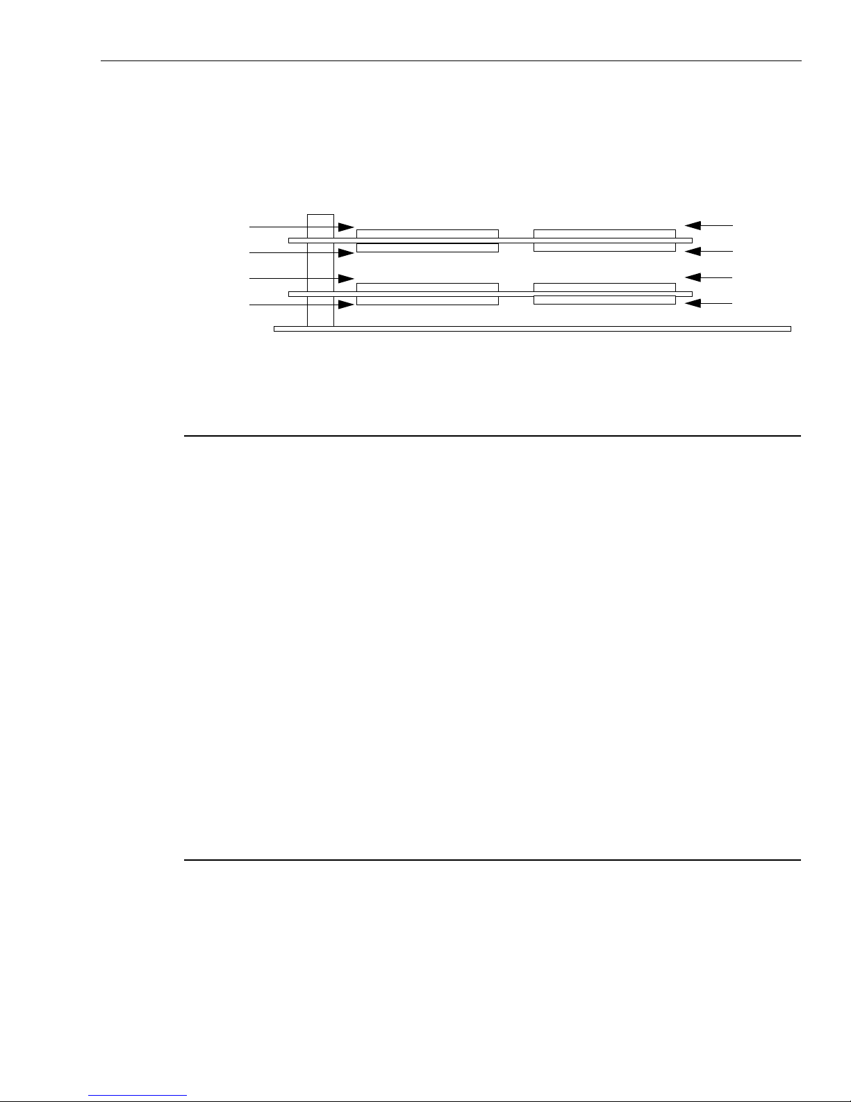
Themis Computer 4-5
4. Hardware Overview
10-bit column addressing is supported on the modules. Considerable attention was paid to minimize the power
consumption of USPIIi-1v. The maximum active power consumption of a 64 MB memory module is 4.212
watts.
.
Figure 4-1. Memory Sub-System Topology
4.3 PMC Carrier Subsystem
The PMC Carrier Board subsystem supports up to three (3) standard PMC boards in either the second or third
slot of the USPIIi-1v product configuration. If the I/O board or Creator Graphics card is included in the
product configuration (USPIIi-1v/3), the PMC carrier board is physically located in the third slot. Otherwise,
the PMC Carrier board is located in the second slot (USPIIi-1v/2p).
In addition to the standard PMC I/O, 64 bits of configurable User I/O are provided from the VME P2
connector directly to the PMC #1 and PMC #2 board positions. All 64 bits may be routed to PMC #1, leaving
0 bits of User I/O for PMC #2. Or, 32 bits may be routed to PMC #1 and to PMC #2. In the latter case, PMC
#1 will utilize the upper VME P2 signals, VME P2 A[32..17] and VME P2 C[32..17] while PMC #2 will
utilize the lower VME P2 signals, VME P2 A[16..1] and VME P2 C[16..1]. The signals are available on the
J5 connector of PMC #1 and the J8 connector of PMC #2. If all 64 bits of User I/O are routed to PMC #1, it
utilizes all 64 signals of the VME P2 connector. In this case, all 64 signals are available on the J5 connector
of PMC #1. For a diagram illustrating the locations of the various connectors and the PMC carrier slots
Section D.3, "PMC Board," on page D-6.
The selection of the User I/O signal routing is performed by installing a User I/O adapter card on J11 and J12
of the PMC Carrier board. If the adapter card is left uninstalled all 64 bits of User I/O are routed to PMC #1.
If the adapter card is installed, 32 bits of User I/O are routed to PMC #1 and 32 bits of User I/O are routed to
PMC #2. Consult the factory for that option.
4.4 OpenBoot PROM
The OpenBoot PROM (OBP) can be accessed through the EBus2. OBP code is contained in Flash Memory
and provides the following functionality:
• Runs start-up diagnostic tests.
• Initializes the host machine.
Bank #0
Bank #2
Bank #3
Bank #1
Bank #7
Bank #5
Bank #4
Bank #6

USPIIi-1v Hardware Manual
4-6
Themis Computer
• Reads non-volatile RAM (NVRAM) and executes the boot sequence. The Diagnostic Executive or
standalone programs can also be executed.
• Includes the abbreviated system monitor. Entry into the system monitor is signified by the “ok” prompt.
If a boot attempt fails, the OBP tries to start the abbreviated system monitor.
• Supplies program code for the FORTH Toolkit; the on-board diagnostics contain the FORTH Toolkit
and the FORTH language interpreter. Entry into the FORTH Toolkit is signified by the “ok” prompt.
For more information on the OBP please refer to the OpenBoot Command Reference from Sun Microsystems
and to the “USPIIi-1v Software Manual”.

5.1 Features
Tundra’s Universe IIB (CA91C142) interfaces the local 32-bit PCI bus to the VMEbus. The following lists
some of the Universe IIB’s features on the USPIIi-1v board:
• 33 MHz, 32-bit PCI bus interface
• Fully compliant, high performance 64-bit VMEbus interface
• Integral FIFOs buffer with multiple transactions from the PCI bus to the VMEbus and from the
VMEbus to the PCI (both directions)
• Programmable DMA controller with linked list support
• A broad range of VMEbus address and data transfer modes:
5
5Universe-IIB Description
– A32/A24/A16 master and slave transfer, except for A64 and A40
– D64/D32/D16/D08 master and slave transfer, except for MD32
– MBLT, BLT, ADOH, RMW, LOCK, and location monitors
• Support for full VMEbus System Controller
• Nine user programmable slave images on the VMEbus and the PCI bus ports
• Seven interrupt lines
• Auto initialization for the slave only applications
• Programmable registers from both the VMEbus and the PCI bus
• Support for four mailbox registers
• Support for four location monitors
• Support for eight semaphores
• Support for RMW cycles and lock cycles
This chapter is intended to outline the VMEbus to PCI Bus interface on the USPIIi-1v. If more detailed
information is need, please refer to the Tundra “Universe II User’s Manual”, Spring 1998.
Note — All registers on the Universe IIB are little-endian.
Themis Computer 5-1

USPIIi-1v Hardware Manual
5.2 USPIIi-1v and the Universe IIB PCI Interface
The following table lists some of the PCI signals of the USPIIi-1v to the Universe IIB’s PCI interface.
Table 5-1. Universe IIB PCI Interface Pins
USPIIi-1v
Universe IIB Pins
AD[31..0] AAD<31..0> 32-bit PCI Bus interface
LCLK U2_CLK 33MHz
IDSEL AAD<12> Primary PCI Bus Address 12
REQ# AREQ_L<0> PCI Bus Request 0
GNT# AGNT_L<0> PCI Bus Grant 0
LINT_0# U2_LINT_L<0> PCI IRQ 0
LINT_[7..1]# Pulled up. Unused PCI IRQs
Primary PCI Bus
Signals
Description
5.3 VMEbus Interface
5.3.1 VMEbus Configuration
The following lists the initial configuration of the VMEbus system:
• VMEbus First Slot Detector
• Two methods of Auto Slot ID
• Register Access at the power up
5.3.2 Universe IIB as the VMEbus Slave
The Universe IIB’s VMEbus Slave Channel supports all of the addressing and data transfer modes which are
documented in the VME64 specification. The Universe IIB does not support the A64 mode and the modes
intended to augment the 3U applications, i.e. A40 and MD32. The Universe II becomes a slave when one of
its eight programmed slave images or register images are accessed by a VMEbus master. It is not implied that
the Universe II cannot reflect a cycle on the VMEbus and access itself, as it is capable of doing so. Depending
on the programmed values of the VMEbus slave images, the incoming write transaction from the VMEbus
may be treated as either posted or coupled (refer to Section 5.4, "Slave Image Programming," on page 5-7). If
the post write operation is selected, the data is written to a Posted Write Receive FIFO (RXFIFO) and the
VMEbus master receives the data acknowledgment from the Universe IIB. The Universe IIB transfers the
write data from the RXFIFO without the involvement of the initiating VMEbus master (refer to “Posted
Writes” on page 2-15 of the Universe IIB manual for a complete explanation of this operation). If the coupled
5-2 Themis Computer

5. Universe-IIB Description
cycle operation is selected, the transaction is completed on the PCI bus first, and the data acknowledgment is
sent to the VMEbus master. With the coupled cycle, the VMEbus is not available to other masters while the
PCI bus is executing the transaction.
Read transactions may either be pre-fetched or coupled. A pre-fetched read is initiated when enabled by the
user and a VMEbus master requests for a block read transaction (BLT or MBLT). When the Universe IIB
receives a request for the block transfer, it begins to fill its Read Data FIFO (RDFIFO) using burst
transactions from the PCI bus resource. The initiating VMEbus master then obtains its block read data from
the RDFIFO of the Universe IIB rather than the PCI resources directly.
A RMW cycle allows a VMEbus master to read from a VMEbus slave and then write to the same resource
without releasing the bus between the two operations. Each one of the Universe IIB slave images can be
programmed to map RMW cycles to the PCI Locked cycles. RWM cycles are not supported with the
unaligned or D24 Cycles.
In order to support the VMEbus broadcast capability, Universe IIB has four Location Monitors. The location
monitor’s image consist of a 4Kbyte image in A32, A24, or A16 space on the VMEbus. If the Location
Monitor is enabled, an access to a Location Monitor would cause the PCI Master Interface to issue an
interrupt.
The Universe IIB supports the VMEbus lock commands as they are described in the VME64 Specification.
The ADOH cycles are used to execute the lock command with a special AM code. A locked resource can not
be accessed by any other resource as long as the VMEbus master has the bus ownership. It Target-Abort or
Master-Abort occurs during a locked transaction on the PCI bus, the Universe IIB will reliquaries its lock on
the bus, in accordance with the PCI Specification.
5.3.3 Universe IIB as the VMEbus Master
The Universe IIB becomes the VMEbus master when the VMEbus Master Interface is internally requested by
the Interrupt Channel, the PCI Bus Target Channel, or the DMA channels. The Interrupt Channel always has
the highest priority over the other two channels and will request the VMEbus Master Interface when it
receives an enabled VMEbus interrupt request.
The PCI Bus Target Channel and the DMA Channel compete for the VMEbus Master Interface and are
awarded it in a fair manner. There are several methods available for user to configure the relative priority that
the DMA channel and the PCI Bus Target Channel have over the VMEbus Master Interface. The PCI Target
Channel requests the VMEbus Master Interface when:
• the TXFIFO contains a completed transaction
• if there is a coupled cycle request.
The DMA Channel requests the VMEbus Master Interface when:
• the DMAFIFO has 64 bytes available when reading from the VMEbus
• the DMAFIFO has 64 bytes in its FIFO when writing to the VMEbus
• the DMA block is complete.
Themis Computer 5-3

USPIIi-1v Hardware Manual
PCI
Master
Bi-Directional DMA FIFO
VMEbus Slave Channel
posted writes
pre-fetch reads
coupled read
VME
Slave
PCI Bus
PCI
Slave
PCI Bus Slave Channel
posted writes with FIFO
coupled read logic
VME
Master
VMEbus
Interrupt Channel
PCI
Interrupts
Interrupt Handler
Interrupter
VME
Interrupts
Bi-Directional DMA FIFO
Figure 5-1. Universe IIB Architectural Diagram
The Universe IIB’s VMEbus Master Interface supports all of the addressing and data transfer modes as
specified by the VME64 specification. The Universe IIB does not support the A64 mode and modes intended
to augment the 3U applications, i.e. A40 and MD32. The Universe IIB is compatible with all the VMEbus
modules that conform to pre-VME64 specification. The Universe IIB as the VMEbus Master supports RMW,
and ADOH. The Universe IIB accepts BERR# and DTACK# as cycle terminations from the VMEbus.The
Universe IIB does not accept the RETRY# as a termination from the VMEbus Slave. DTACK# indicates the
successful completion of a transaction. The Universe IIB utilizes the ADOH cycle to implement the VMEbus
Lock command allowing a PCI bus master to lock the VMEbus resources.
5.3.4 VMEbus First Slot Detector
As defined by the VME64 specification, the Universe IIB samples the BG3IN# right after the reset to
determine if the USPIIi-1v resides in slot 1. If the BG3IN# is sampled low right after the reset, the USPIIi-1v
board becomes the SYSCON. Otherwise the SYSCON Module of the Universe IIB is disabled. The software
can set or clear the SYSCON bit the MISC_CTL register of the Universe IIB. The definition of the
MISC_CNT register is provided in Table 5-2, "Universe IIB Miscellaneous Control Register (MISC_CTL),"
on page 5-4. The offset of this register is 0x404.
Table 5-2. Universe IIB Miscellaneous Control Register (MISC_CTL)
BIts Name Description Reset
[31:28] VBTO VMEbus Time-out:
26 VARB VMEbus Arbitration Mode: 0 = Round Robin; 1 = Priority 0 R/W
5-4 Themis Computer
a
Access
State
0011 R/W
0000 = Disable; 0001 = 16 µs; 0010 = 32 µs; 0011 = 64 µs;
0100 = 128 µs; 0101 = 256 µs; 0110 = 512 µs;
0111 = 1024 µs; Others = RESERVED

5. Universe-IIB Description
Table 5-2. Universe IIB Miscellaneous Control Register (MISC_CTL)
BIts Name Description Reset
[25:24] VARBTO VMEbus Arbitration Time-out
00 = Disable Timer; 01 = 16 µs (minimum value of 8 µs,
due to the 8 µs clock granularity); 10 = 256 µs;
others - RESERVED
23 SW_LST PCI Reset: 0 = no effect; 1 = initiate PCI bus LRST# 0 W
22 SW_SYSRST Software VMEbus SYSRESET: 0 = no effect; 1 = Initiate
VMEbus SYSRST
20 BI BI- Mode: 0 = Universe IIB is in BI-mode;
1 = Universe IIB is not in BI mode
19 ENGBI Enable Global BI-mode Initiator:
0 = Assertion of VIRQ1 ignored; 1 = Assertion of VIRQ1
puts the Universe IIB in BI-mode
18 RESCIND Unused on the Universe IIB 1 R/W
17 SYSCON SYSCON:
0 = Universe IIB is not a VMEbus System Controller;
1 = Universe IIB is a VMEbus System Contoller
16 V64AUTO VME64 Auto ID:
Write: 0 = no effect; 1 = Initiate sequence
This bit initiates the Universe IIB VME64 Auto ID Slave par-
ticipation.
a
Access
State
01 R/W
0 W
Power-up
Option
0 R/W
Power-up
Option
Power-up
Option
R/W
R/W
R/W
a. All unspecified bits in this table are RESERVED for the Universe IIB and should not be accessed by the user.
When the Universe IIB is configured as the System Controller, it provides the following functions on the
VMEbus:
– A 16MHz Clock Driver
– An Arbitration Module
– A bus timer
– An IACK Daisy Chain Driver (DCD).
The USPIIi-1v supports Round-Robin arbitration. The VMEbus arbitrator time out is also controlled by the
MISC_CNT register described above. The timer may be set to either 16 µs, 256 µs, or disabled. The default
setting is 16 µs. The arbitration timer has a granularity of 8 µs; setting the timer to 16 µs means the timer
may expire in as little as 8 µs or as much as 24 µs. It should also be noted that disabling the arbitration timer
implies that the Universe IIB will not recover from an access error. Disabling the arbitration timer is not
recommended.
5.3.4.1 Automatic Slot Identification
The Universe IIB supports two types of Auto ID functionality:
• Auto Slot ID as described by the VME64 specification
• Proprietary Method which is developed by Tundra
Themis Computer 5-5

USPIIi-1v Hardware Manual
Refer to “Auto Slot ID: VME64 Specified”, on page 2-24, and “Auto-ID: A Proprietary Tundra Method”, on
page 2-25 of the Universe IIB Manual for more information.
5.3.4.2 Registered Access at the power up
Register access at the power up is used in a system where either the Universe IIB is independent of the local
CPU or there a CPU is not present. Since the Universe IIB and the UltraSPARC-IIi are present on the USPIIi-
1v, registered access at power up is not supported.
5.3.5 Universe IIB’s hardware Power -Up Options
The Universe IIB power up options are determined right after the PWRRST# based on the level of VMEbus
Address VA[31..1] and VMEbus Data VD[31..27]. Table 5-3, "Address Translation for PCI Bus to VMEbus
Transfers," on page 5-10 for the Universe IIB’s power up options on the USPIIi-1v.
The Universe IIB is automatically configured at power up to operate in the default configuration listed in
Table 5-3, "Universe IIB Power Up Options ," on page 5-6. It should be noted that all power up options are
latched only at the positive edge of PWRRST#; they are loaded when SYSRST#, PWRRST#, and RST# are
negated.
Table 5-3. Universe IIB Power Up Options
Option Register Field Default Pins
VMEbus Register
Access Slave
Image
VMEbus CR/CSR
Slave Image
Auto-ID MISC_STAT DY4AUTO Disabled VD[30]
BI-Mod) MISC_CTL BI Disabled VD[28]
AUTO_SYSCON
Detect
SYSFAIL# Asser-
tion
PCI Target IMAGE LSI0_CTL EN Disabled VA[13]
VRAI_CTL EN Disabled VA[31]
VAS A16 VA[30..29]
VRAI_BS BS 0x00 VA[28..21]
VCSR_CTL LAS[0]
VCSR_TO TO 0x00 VA[19..15]
MISC_CTL V64AUTO Disabled VD[29]
VINT_EN SW_INT 0
VINT_STAT SW_INT 0
VINT_MAP1 SW_INT 000
MISC_CTL SYSCON Enabled VBG3IN#
VCSR_SET SYSFAIL Asserted VD[27]
VCSR_CLR SYSFAIL -- --
a
Memory VA[20]
LSI0_BS BS 0x0 VA[9..6]
LSI0_BD BD 0x0 VA[5..2]
5-6 Themis Computer
LAS[0] Memory VA[12]
VAS A16 VA[11..10]

5. Universe-IIB Description
Table 5-3. Universe IIB Power Up Options
Option Register Field Default Pins
PCI Bus Size
PCI CSR Image
Space
b
MISC_STAT LCLSIZE 32-bit REQ64#
PCI_CSR BM Disabled VA[14]
PCI Register
Access
PCI_BS0
PCI_BS1
SPACE Refer to:
Table 5-4 and
VA[1]
Table 5-5 .
PCI Bus Size
PCI CSR Image
c
MISC_STAT LCLSIZE 32-bit REQ64#
PCI_CSR BM disabled VA[14]
Size
a. The LAS field will enable the PCI_CSR registers IOS or MS field if the EN FIELD of the LSIO_CTL register is set.
b. As per PCI 2.1 Specification, the PCI Bus Size is loaded on any RST# event.
c. Following the PCI 2.1 Specification, the PCI Bus Size is loaded on any RST# event.
The PCI Configuration Base Address 0 and Base Address 1 Registers offsets are 0x010 and 0x014,
respectively. The registers specify the 4KB aligned base address of the 4 KB Universe IIB register space on
PCI. The power-up options determine if the registers are mapped into Memory or I/O space.
Table 5-4. PCI Configuration Base Address 0 Register (PCI_BS0)
BIts Name Description Reset
[31:12] BS Base Address 0 R/W
00 SPACE PCI Bus Address Space: 0 = Memory; 1 = I/O Power-up
a
Access
State
R
Options
a. All other bits are Read 0.
Table 5-5. PCI Configuration Base Address 1 Register (PCI_BS1)
BIts Name Description Reset
[31:12] BS Base Address 0 R/W
00 SPACE PCI Bus Address Space: 0 = Memory; 1 = I/O Power-up
a. All other bits are Read 0.
5.4 Slave Image Programming
The Universe II recognizes two types of accesses on its bus interfaces: accesses destined for the other bus and
accesses decoded for its own register space.
a
Access
State
R
Options
Themis Computer 5-7
USPIIi-1v Hardware Manual
5.4.1 VME Slave Images
A VMEbus slave image is used to access the resources of the PCI bus when the Universe II is not the
VMEbus master. The user may control the type of accesses by programming specific attributes of the
VMEbus slave image. The Universe II will only accept accesses to the VMEbus from with the programmed
limits of the VMEbus slave image.
Note — The Bus Master Enable (BM) bit of the PCI_CS register must be set in order for the image to
accept posted writes from an external VMEbus master. If this bit is cleared while there is data in the
VMEbus Slave Posted Write FIFO, the data will be written to the PCI bus. No further data is accepted into
this FIFO until the bit is set.
5.4.1.1 VMEbus Fields
Before the Universe II responds to a VMEbus Master (other than itself), the address must lie between the base
and bound addresses. Also, the address modified must match modifier specified by the address space, access
mode, and type fields. A description of the VMEbus fields for VMEbus Slave Images in presented in Table 56, "VMEbus Fields for VMEbus Slave Image," on page 5-8.
The Universe II’s eight VMEbus slave images (0-7) are bounded by A32 space. Slave images 0 and 5 have a
4 KB resolution. Typically, these images would be used as an A16 image since they provided the finest
granularity. Slave images 1 to 3 and 6 to 8 have a 64 KB resolution. The maximum image size of 4 GB.
Field Register Bits Description
base BS[31:12] or BS[31:16] in VSIx_BS Multiples of 4 or 64 KBytes (base to
bound BD[31:12] or BD[31:16] in VSIx_BD
address space VAS in VSIx_CTL A16, A24, A32, User 1, User 2
mode SUPER in VSIx_CTL Supervisor and /or non-privileged
type PGm in VSIx_CTL Program and/or data
Warning —!The address space of a VMEbus slave image must not overlap with the address space for the
Universe II’s control and status registers.
5.4.1.2 PCI Bus Fields
The PCI bus fields specifies the mapping of a VMEbus transaction to the appropriate PCI bus transaction and
allows users to translate a VMEbus address to a different address on the PCI bus. The translation of VMEbus
transactions beyond 4 GB results in a wrap-around to the low portion of the address range.
Table 5-6. VMEbus Fields for VMEbus Slave Image
bound: maximum of 4 GB)
Table 5-7. PCI Bus Fields for VMEbus Slave Image
Field Register Bits Description
Translation Offset TO[31:12] or TO[31:16] in
5-8 Themis Computer
VSIx_TO
Offsets VMEbus slave address to a
selected PCI address

5. Universe-IIB Description
Table 5-7. PCI Bus Fields for VMEbus Slave Image
Field Register Bits Description
Address space LAS in VSIx_CTL Memory, I/O, Configuration
RMW LLRMW in VSIx_CTL RMW enable bit
A32 Image
5.4.1.3 Control Fields
A VMEbus slave image is enabled using the EN bit of the control field. The control field also specifies how
reads and writes are processed: either as a coupled transfer or a posted write. At power up, all images are
disabled and configured for coupled reads and writes.
Field Register Bits Description
image enable EN in VSIx_CTL enable bit
posted write PWEN in VSIx_CTL posted write enable bit
Offset [31..12]
VME [31..12] VME[11..0]
+
PCI [11..0]PCI [31..12]
Figure 5-2. Address Translation for VMEbus to PCI Bus Transfers
Table 5-8. Control Fields for VMEbus Slave Image
prefetched read PREN in VSIx_CTL prefetched read enable bit
enable PCI64 LD64EN in VSIx_CTL enables 64-bit PIC bus transactions
Note — For a VMEbus slave image to respond to an incoming cycle, the PCI Master Interface must be
enabled (bit BM in the PCI_CSR register).
5.4.2 PCI Bus Target Images
The Universe II accepts accesses from the PCI bus with specific programmed PCI target images that open
windows to the VMEbus and control to the type of access to the VMEbus. There are eight (0-7) standard PCI
target images and one special PCI target image. The special PCI target image may be used for A16 and A24
transaction, freeing the other 8 images for standard A32 transactions.
Themis Computer 5-9
USPIIi-1v Hardware Manual
5.4.2.1 PCI Bus Fields
Decoding for VMEbus accesses is based on the address and command information produced by a PCI bus
master. The PCI Target Interface claims a cycle if there is an address match and if the command matches
certain criteria.
The PCI target images are A32-capable only. For accesses other than A32 the Special PCI Target Image may
be used (refer to Section 5.4.2.4, "Special PCI Target Image," on page 5-11). Of the eight standard PCI target
images, the first and fifth (PCI target images 0 and 4) have a 4 KB resolution. PCI target images 1 to 3 and 5
to 8 have a 64 KB resolution.
Field Register Bits Description
base BS[31:12] or BS[31:16] in LSIx_BS Multiples of 4 or 64 KBytes (base to
bound BD[31:12] or BD[31:16] in LSIx_BD
address space LAS in LSIx_CTL Memory or I/O
Warning —!The address space of a VMEbus slave image must not overlap with the address space for the
Universe II’s control and status registers.
Table 5-9. PCI Bus Fields for PCI Bus Target Image
bound: maximum of 4 GB)
5.4.2.2 VMEbus Fields
The VMEbus fields cause the Universe II to generate the appropriate VMEbus address, AM code, and cycle
type, allowing PCI transactions to be mapped to a VMEbus transaction. It is possible to use invalid
combinations, such as block transfers in A16 space. This may cause illegal transactions on the VMEbus. All
accesses beyond the 4 GB limit will wrap around to the low address range
.
A32 Image
Offset [31..12]
VME [31..12] VME[11..0]
+
PCI [11..0]PCI [31..12]
Figure 5-3. Address Translation for PCI Bus to VMEbus Transfers
5-10 Themis Computer

Field Register Bits Description
base BS[31:12] or BS[31:16] in LSIx_BS Translates PCI Bus Address to
bound BD[31:12] or BD[31:16] in LSIx_BD 8, 16, 32, or 64 bits
address space LAS in LSIx_CTL A16, A24, A32, User 1, User 2
mode SUPER in LSIx_CTL Supervisor or non-privileged
type PGM in LSIx_CTL Program or data
cycle VCT in LSIx_CTL Single or Block
5.4.2.3 Control Fields
Through the control fields, the user specify how writes are processes and enable a PCI target image. The PCI
target image is enabled by setting the EN bit.
5. Universe-IIB Description
Table 5-10. PCI Bus Fields for PCI Bus Target Image
VMEbus Address
Posted Writes are performed when the PWEN bit is set and the particular PCI target image is accessed. Posted
writes are only decoded within PCI Memory space. Access from other memory spaces are performed with
coupled cycles, regardless of the setting of the PWEN bit.
Table 5-11. Control Fields for PCI Bus Target Image
Field Register Bits Description
image enable EN in LSIx_CTL enable bit
posted write PWEN in LSIx_CTL posted write enable bit
Note — For a VMEbus slave image to respond to an incoming cycle, the PCI Master Interface must be
enabled (bit BM in the PCI_CSR register).
5.4.2.4 Special PCI Target Image
A special PCI target image is provided to expedite A16 and A24 transaction. The other eight, standard, PCI
target images are typically programmed to access A32 space. The special PCI target image is a 64 MB space,
located either within memory or I/O space, that is decoded using PCI address lines [31:26]. Its base address is
aligned on 64 MB boundaries and no offsets are provided. Therefore, PCI address information is mapped
directly to the VMEbus. The special PCI target image has a lower priority than any other PCI target image.
Themis Computer 5-11
USPIIi-1v Hardware Manual
The 64 MB space is divided into four (4), 16 MB spaces that are selected using AD[25:16]. For each region,
the upper 64 KB map to VMEbus A16 space, while the remaining portion map to VMEbus A24 space. The
addressing of this slave image is depicted in Figure 5-2 "Address Translation for VMEbus to PCI Bus
Transfers," on page 5-9.
base BS[05] in 64 MB aligned base address for the
address space LAS in Places Image in Memory or I/O
maximum data width VDW in separately set each region for 16 or
mode SUPER in separately set each region for
type PGM in Program or data
Table 5-12. PCI Bus Fields for Special PCI Bus Target Image
Field Register Bits Description
image
Table 5-13. PCI Bus Fields for Special PCI Bus Target Image
Field Register Bits Description
32 bits
supervisor or non-privileged
cycle VCT in Separately sets each region as pro-
gram or data
.
Table 5-14. Control Fields for Special PCI Bus Target Image
Field Register Bits Description
image enable EN in enable bit
posted write PWEN in posted write enable bit
The special PCI target image register is described below.
Table 5-15. Special PCI Target Image Register (Offset 188)
Bits Name Type Reset
State
31 EN R/W 0 Image Enable
0 = Disable, 1 = Enable
30 PWEN R/W 0 Posted Write Enable
0 = Disable, 1 = Enable
29:24 Reserved
23:20 VDW [3..0] R/W 0 VMEbus Maximum Datawidth. Each of the four bits specifies a
data width for the corresponding 16 MB regions. The lower order
bits correspond to the lower order address regions.
0 = 16 bit, 1 = 32 bit
19:16 Reserved
Description
5-12 Themis Computer

5. Universe-IIB Description
Table 5-15. Special PCI Target Image Register (Offset 188)
Bits Name Type Reset
State
15:12 PGM [3..0] R/W 0 Program/Data AM Code
Each of the four bits specifies Program/Data AM code for the corresponding 16 mB region. The lower order bits correspond to the
lower order address regions.
0 = Data, 1 = Program
11:8 SUPER [3..0] R/W 0 Supervisor/User AM Code
Each of the four bits specifies Supervisor/User AM code for the
corresponding 16 MB region. Lower order bits correspond to the
lower address regions.
0 = Non-Privileged, 1 = Supervisor
07-02 BS [5..0] R/W 0 Base Address
Specifies a 64 MB aligned base address for this 64 MB image
01 Reserved
00 LAS R/W 0 PCI Bus Address Space
0 = PCI Bus Memory Space, 1 = PCI Bus I/O Space
Description
Themis Computer 5-13

USPIIi-1v Hardware Manual
64 MB
BASE+0x400.0000
BASE+0x3FF.FFFF
BASE+0x300.0000
BASE+0x2FF.0000
BASE+0x200.0000
BASE+0x1FF.0000
BASE+0x100.0000
BASE+0x0FF.0000
A16
3
A24
16 MB
A16
2
A24
A16
1
A24
A16
0
A24
BASE+0x000.0000
Figure 5-4. Memory Mapping in the Special PCI Target Image
5.5 Universe IIB’s Interrupt and Interrupt Handler
5.5.1 VME and PCI Interrupters:
For the VMEbus, the interrupt source can be mapped to any of the VMEbus interrupt output pins such as
VIRQ#[7..0]. If a hardware and software source are assigned to the same VMEbus VIRQn# pin, the software
source always has higher priority. Interrupt sources mapped to the PCI bus interrupts are generated via the
PCI Interrupt pin, INT#0.
For the VMEbus interrupt outputs, the Universe IIB interrupter provides an 8-bit STATUS/ID to a VMEbus
interrupt handler. Optionally, the Universe IIB generates an internal interrupt to signal that the interrupt vector
has been provided.
5-14 Themis Computer

Interrupts mapped to the PCI bus interrupt output pin (INT0#) are serviced by the PCI Interrupt Controller.
The UltraSPARC-II i determines which interrupt sources are active by reading the interrupt status register in
the Universe IIB. The interrupt is negated after being serviced by the UltraSPARC-IIi.
5.5.2 VMEbus Interrupt Handling:
A VMEbus interrupt causes the Universe IIB to issue a normal VMEbus IACK cycle and to generate the
specified interrupt output. When the IACK cycle is completed, the Universe IIB relinquishes the VMEbus.
The interrupt vector is read by the PCI resource servicing the interrupt output. Hardware and internal
interrupts are RORA. Software interrupts are ROAK.
5.5.3 Universe IIB’s Mailbox Registers:
Universe IIB contains four 32-bit mailbox registers that provide an additional communication path between
the PCI bus and the VMEbus. The mailboxes support read and write accesses from either bus. The mailboxes
may be enabled to generate interrupts on either bus whenever written to. The mailboxes are accessed from the
same address spaces and in the same method as other Universe IIB registers.
5. Universe-IIB Description
5.5.4 Universe IIB’s Semaphores
The Universe IIB contains two general purpose semaphore registers such as SEMA0 and SEMA1; each
register contains four semaphores. To obtain the ownership of a semaphore, a processor writes a logic one to
the semaphore bit and an unique pattern to the associated tag field; if a subsequent read of the tag field returns
the same pattern, then the processor has gained the ownership of the semaphore. In order to release the
semaphore, the processor writes a value of 0 to it.
5.5.5 Programmable slave images on the VMEbus and PCI bus:
There are two types of accesses that the Universe IIB recognizes on its bus interfaces: accesses for its own
register space and accesses destined elsewhere.
For the VME Slave Images, the Universe IIB accepts accesses from the VMEbus within specific programmed
slave images. Each one of the VMEbus slave image opens a window to the resources on the PCI bus, and
through the specific attributes, the VMEbus slave images allow the user to control the type of access to the
PCI resources. The VMEbus slave images are divided into VMEbus, PCI bus, and Control fields (refer to
Section 5.4, "Slave Image Programming," on page 5-7).
For the PCI Slave Images, the Universe IIB accepts accesses from the PCI bus with the specific programmed
PCI target images. Each one of the PCI bus slave image opens a window to the resources on the VMEbus, and
it allows the user to control the type of access to the VMEbus resources. The PCI bus slave images are
divided into VMEbus, PCI bus, and control fields. There is one special PCI target image which is separate
from the VMEbus, PCI bus, and the control fields (refer to Section 5.4, "Slave Image Programming," on page
5-7).
Themis Computer 5-15

USPIIi-1v Hardware Manual
5.5.6 DMA Controller
The Universe IIB utilizes an internal DMA controller for high performance data transfer between the
VMEbus and the PCI bus. Universe IIB’s parameters for the DMA transfer are software configurable. DMA
operations between the source and destination bus are decoupled via the use of a single bidirectional FIFO
(DMAFIFO).
There are two modes of operation for the DMA: Linked List Mode and Direct Mode. In Linked List Mode,
the Universe IIB loads the DMA registers from PCI memory and executes the transfers described by these
registers. In the direct mode, the PCI master directly programs the DMA registers.
The DMA controller also utilizes the command packet. A command packet is a block of DMA registers stored
in PCI memory. A command packet may be linked to another command packet so that when the DMA has
finished the operations described by one command packet, the DMA controller can automatically move on to
the next command packet in the linked-list of command packets (refer to “DMA Controller” on page 2-77 of
the Universe II User’s Manual).
5-16 Themis Computer

Themis Computer 6-1
6
6FPGA, Watchdog, Voltage and Temperature Sensors
6.1 FPGA
6.1.1 Introduction
The FPGA device on the USPIIi-1v is the Altera EPF882 and resides on the EBus2 of the baseboard PCI I/O
ASICs. Physically, the FPGA is located on the baseboard. The FPGA implements a voltage monitor, boot
address decoder, a three-level watchdog timer, and the READY_LED register. At boot-up the FPGA self
loads from a serial EPROM (Altera EPC1213PC8) to program itself for these features.
Full description of the FPGA registers is presented in the “USPIIi-1v Software Manual”.
6.1.2 Boot Address Decoder
The Flash EPROM logic is made of 3 Flash devices:
• System Flash (2MB or 4 MB) is loaded at factory with OpenBoot for the Sun Configuration
• User Flash 1 (4 MB) is loaded at factory with OpenBoot for the PS/2 Configuration
• User Flash 2 (4 MB) is not loaded
Depending on the board configuration, either System Flash/User Flash 2 (in PS/2 Configuration) or User
Flash 1/User Flash 2 (in Sun configuration) will be available for user programs or data. The USPIIi-1v
OpenBoot contain special commands to program Flash devices, please refer to the USPIIi-1v Software
Manual.

USPIIi-1v Hardware Manual
6-2
Themis Computer
The Boot Address Decoder selects between boot access of the System Flash, the ROMBO connector, or User
Flash 1. Selection is made by jumpers J3303 and J3304. The tables below
show the address maps related to the
PCIO’s internal address space for all jumper combinations.
The device mapped in Address Space will be the
USPIIi-1v boot device.
Selection between System Flash or ROMBO is made through jumper J3303:
6.1.3 3-Level Watchdog
A 3-level watchdog is implemented in the FPGA. The states of the watchdog are “normal”, “warning”,
“coping”, and “failed”. Each watchdog may be programmed to expire within the range of 0.1 seconds to
approximately 6500 seconds and contains a 16-bit counter register, 16-bit a limit register, and an 8-bit status
register. The counter register and the status register are read-only while the limit register is read/write. Refer
to the “USPIIi-1v Software Manual” for a description of the Watchdog Registers.
Note —
The 3-level watchdog implemented in the FPGA is entirely separate from the internal watchdog of
the UltraSPARC-IIi. For more information on the watchdog implemented in the UltraSPARC-IIi refer to
Section 7.2.3, "Watchdog Reset (WDR)," on page 7-2 or the UltraSPARC-IIi User’s Manual, published by
SUN Microelectronics (SME).
Table 6-1. Mapping of Flash Devices: J3304 on 2-3 or removed (Boot from System Flash)
Address Space Address Range Device Access
0 0x00.0000 - 0x3F.FFFF System Flash/ROMBO Read/Write
b
1 0x40.0000 - 0x7F.FFFF User Flash 1 Read/Write
a
2 0x80.0000 - 0xBF.FFFF User Flash 2 Read/Write
a
Table 6-2. Mapping of Flash Devices: J3304 on 1-2 (Boot from User Flash)
Address Space Address Range Device Access
0 0x00.0000 - 0x3F.FFFF User Flash 1 Read/Write
a
a. In order to write to the User Flash, jumper JP3302 must be set to position 2-3.
1 0x40.0000 - 0x7F.FFFF User Flash 2 Read/Write
a
2 0x80.0000 - 0xBF.FFFF System Flash/ROMBO Read/Write
b
b. In order to write to the System Flash, jumper JP1401 must be set to position 2-3.
Table 6-3. Jumper J3303 setting
Jumper J3303 Setting Address Space Assignment
1-2 ROMBO
2-3 or Not Installed (Default) System Flash

Themis Computer 6-3
6. FPGA, Watchdog, Voltage and Temperature Sensors
When no watchdogs have expired the USPIIi-1v is in a ‘normal’ state. When the level 1 watchdog expires, a
maskable interrupt is sent to the RIC. The USPIIi-1v is considered to be in a ‘warning’ state. Upon expiration,
the level 2 watchdog issues a non-maskable XIR interrupt to the RIC. This signal has the same effect as an
“Abort” button assertion and will terminate the active job. When this occurs the board is considered to be in
a ‘coping’ state.
The level 3 watchdog causes a “serious alarm condition” when it expires. The USPIIi-1v is then considered to
be in a ‘failed’ state. This signal is connected to the backplane of the board. This signal will generate a non-
maskable Power-On-Reset to be issued to the UltraSPARC-IIi and propagated throughout the system. This
reset may be disabled by setting jumper J3301. If jumper J3301 is set to 1-2 the reset is enabled. If jumper
J3301 is set to 2-3 the reset is disabled.
Expiration of watchdog level 2 will turn the front panel ALARM LED to amber. Expiration of watchdog level
3 will turn it to red and cause the assertion of the SW ALARM pin on VME P2. See Appendix A.2.2,
"Baseboard VME P2," and Appendix A.2.9, "LEDs."
Upon expiration, any higher-order watchdog will reset a lower-order watchdog, i.e.: the expiration of
watchdog 3 resets watchdog 1 and watchdog 2 to their initial, programmed states.
The entire 3-Level Watchdog may be disable through the setting of solder bead SB3302. When solder bead
SB3302 is installed (shorted) the watchdog is enabled. When solder bead SB3302 is open, the watchdog is
disabled.
6.1.4 Power Management System
A voltage monitor is implemented in the FPGA and with external circuitry. The USPIIi-1v voltage monitor
has three states: normal, coping, and failed. The +5V, +3.3V and +1.9V signals are monitored for drops of -
5% and -10%. The voltage monitor is in a normal state if all three voltage levels are within 5% of nominal.
The voltage monitor is in a coping state if any of the signals drop below -5%. If the voltage monitor is in the
coping state for longer than 100 milliseconds, the FPGA will generate an XIR interrupt to the RIC. If the
voltage monitor is in the coping state for longer than 500 milliseconds, the ‘Functional Bit’ of the FPGA
status register is set.
If a voltage drop of more than -10% for more than 100 milliseconds is detected the board will enter the
‘failed’ state. When entering the failed state the USPIIi-1v’s FPGA will shut down both the 3.3V and the 1.9V
DC-DC power converters, in order to protect the board from damage. It is necessary to cycle the power in
order to recover from this type of shutdown.
Table 6-4. Watchdog POR Enable/Disable
Jumper J3301 Setting Description
Installed 1-2 or Not installed (Default) Disable Reset
Installed 2-3 Enable Reset
Table 6-5. Watchdog Enable/Disable
Solder Bead SB3302 Setting Description
Installed 3-Level Watchdog Enabled
Open (Default) 3-Level Watchdog Disabled

USPIIi-1v Hardware Manual
6-4
Themis Computer
Power Management System entering coping state will turn the front ALARM LED to amber. In failed state,
the LED will turn RED and the POWER FAIL signal will be asserted on VME P2. See Appendix A.2.2,
"Baseboard VME P2," and Appendix A.2.9, "LEDs." The POWER FAIL signal on P2 will also be asserted if
VME ACFAIL is active.

Themis Computer 6-5
6. FPGA, Watchdog, Voltage and Temperature Sensors
6.2 Temperature Sensor
The temperature sensor is implemented using registers in the FPGA and the Dallas Semiconductor DS1620
Digital Thermometer and Thermostat. The Dallas DS1620 provides 9-bit temperature readings which indicate
the temperature of the device. The Dallas DS1620 device is located close to the UltraSPARC-IIi to provide an
accurate reading of the temperature around the processor.
Two user defined temperatures are stored in the Dallas DS1620’s NVRAM: temp-warning and temp-critical.
These variables may be configured by through OBP extension variables (refer to the “USPIIi-1v Software
Manual”). The settings of temp-critical and temp-warning are stored in the 8-bit TL and 8-bit TH registers of
the DS1620.
Warning —!Do not re-configure the temperature warning settings on the USPIIi-1v. Altering these
variables may seriously damage the product. If there are problems with the temperature sensor on the
board, contact Themis Customer Service immediately.
Temperature sensor reaching warning temperature will turn the front ALARM LED to amber. At critical
temperature, the LED will turn RED and the HI TEMP signal will be asserted on VME P2. See Appendix
A.2.2, "Baseboard VME P2," and Appendix A.2.9, "LEDs."

USPIIi-1v Hardware Manual
6-6
Themis Computer

Themis Computer 7-1
7
7Resets
7.1 Overview
This chapter presents a brief discussion of the reset structure of the USPIIi-1v. The various types of resets,
some possible reset sources, and reset effects are explained.
Resets are used to force all or part of the system into a known state. A Reset is defined as any action or signal
that places the UltraSPARC-IIi in Reset, Error, and Debug State (RED_State). This state will be entered under
any of the following conditions:
• A Trap is taken when:
– Trap_Level = Max_Trap_Level - 1
• One of the Reset request signals (POR, XIR, WDR) becomes active
• A reset request, SIR, is issued when the Trap_Level < Max_Trap_Level (If Trap_Level =
Max_Trap_Level, the UltraSPARC-IIi enters and error_state)
• Internal_processor_error exception or catastrophic_error exception occurs
• The setting of PSTATE.RED by system software
The RED_state is indicated by the PSTATE.RED bit being set. For more information on the RED_state
consult Section 17.3, RED_state, of the UltraSPARC-IIi User’s Manual.
The USPIIi-1v reset tree uses the UltraSPARC-IIi CPU in conjunction with the SME Reset, Interrupt, and
Clock chip (RIC), an FPGA, EPLD, and the Universe IIB VMEbus Interface ASIC. The FPGA monitors the
power system and EPLD, as well as receives input from the push-button reset to set the B_POR bit in the
Reset_Control_Register (Table 7-1 ‘UltraSPARC-IIi Reset_Control Register,’ on page 7-5). When any of the
system voltage are out of their nominal ranges, or when the FPGA is self-programming itself, the FPGA
asserts a signal (POWER_OK) to the EPLD. The EPLD passes this signal directly to the RIC which issues a
system reset to the FPGA. The FPGA passes this signal to the UltraSPARC-IIi which places the system in a
reset state until all voltages are with their specified ranges and the FPGA is fully configured.
The FPGA also receives input from the Push-Button Reset. When the FPGA receives this signal it issues a
Push-Button POR to the RIC which, in turn, issues a POR to the UltraSPARC-IIi. The UltraSPARC-IIi will
then place the system in a reset state.

USPIIi-1v Hardware Manual
7-2
Themis Computer
The system, or part of the system, may also be reset by a Watchdog Reset (WDR) or a Software-Initiated
Reset (SIR). These resets originate within the UltraSPARC-IIi core and are only observed by the processor
core. Depending on the conditions and type of the reset, the processor may propagate the reset throughout the
system, in the case of a POR, or reset part of the system, i.e.: the processor core itself.
Note that, unlike other UltraSPARC based systems, the UltraSPARC-IIi does not support a wake-up reset for
power management.
7.2 UltraSPARC-IIi Reset Request Signals
The reset request signals accepted by the UltraSPARC-IIi on the USPIIi-1v board are explained in this
section. The signals are: Power-On Reset (POR), initiated when power is applied to the system or when a
Push-Button Reset is asserted; Externally Initiated Reset (XIR), initiated in response to a signal external to the
UltraSPARC-IIi processor generally indicating a critical system event; Watchdog Reset (WDR), initiated in
response to the error_state; and Software Initiated Reset (SIR), initiated by software with the SIR command.
POR and XIR are received by the UltraSPARC-IIi from the RIC while WDR and SIR are internally generated
by the UltraSPARC-IIi and effect only the processor core. Reset priorities, from highest to lowest are: POR,
XIR, WDR, and SIR.
7.2.1 Power-On Reset (POR)
A POR is a processor and board reset. When POR is active all other resets and traps are ignored. Any pending
external transactions are cancelled.
The UltraSPARC-IIi CPU will propagate this reset to all of the subsystems of the USPIIi-1v, including the ECache, FLASH, UPA64S, and through the Advanced PCI Bridge (APB) to PCI A and PCI B buses to all
other devices. All devices on the board are returned to their initialization states.
7.2.2 Externally Initiated Reset (XIR)
An XIR has a higher priority than all other interrupt, except POR. It is initiated by a source external to the
UltraSPARC-IIi, such as an external component, and propagated to the UltraSPARC-IIi via the RIC. The XIR
preserves the existing state of the board and, if the UltraSPARC-IIi is in error_state, brings it to RED_state. A
system-wide reset does not occur.
7.2.3 Watchdog Reset (WDR)
On the USPIIi-1v a Watchdog Reset (WDR) is generated in response to the error_state of the UltraSPARCIIi. It is generated internally to the UltraSPARC-IIi core. The UltraSPARC-IIi will enter an error_state when
a trap occurs and Trap_Level = Max_Trap_Level - 1. A WDR reset performs a system reset; all pending and
in-progress hardware operations are cancelled or aborted. Hardware and firmware registers are unchanged
from before the WDR but may be in an inconsistent state as some operations have been aborted. If the
processor is in error_state, a WDR places it in RED_state.

Themis Computer 7-3
7. Resets
Note that a WDR reset initiated internal to the processor is different that the 3-Level Watchdog implemented
in the FPGA of the USPIIi-1v. For further explanation of the 3-Level Watchdog Section 7.3.4, "3-Level
Watchdog Resets," on page 7-4.
7.2.4 Software Initiated Reset (SIR)
A Software Initiated Reset is initiated by an SIR instruction from supervisory software. It is initiated within
the UltraSPARC-IIi core and effects only the UltraSPARC-IIi. An SIR is not propagated to the I/O or external
system.
7.3 Reset Sources
The UltraSPARC-IIi accepts two reset signals from the RIC: POR_Reset, and XIR_Reset. The RIC receives
reset signals from the FPGA. The RIC accepts to five resets from the system: Power_OK, Push_Button_POR,
Push_Button_XIR, Scan_POR, and Scan_XIR. Scan_POR and Scan_XIR are used for engineering test
purposes only and not used during the normal operation of the board. POWER_OK is propagated from the
FPGA, through the EPLD, to the RIC. The RIC interprets these signals and issues an appropriate signal, as
explained in succeeding sections.
The UltraSPARC-IIi also accepts SYS_RESET_L from the FPGA. Part of the power management system,
this signal will cause a reset of the USPIIi-1v, as explained below (refer to Section 7.3.2, "Power Management
Resets," on page 7-3).
7.3.1 Push Button Reset
The Push Button Reset is one of the three ways the UltraSPARC-IIi may receive a POR. Push Button Reset
in activated by pressing the push button on the front panel of the USPIIi-1v. This activates the
Push_Button_POR to the RIC. The RIC propagates the signal as a POR to the UltraSPARC-IIi which will
reset the processor. When a Push Button reset in initiated, the B_POR in the Reset_Control_Register (Table
7-1 ‘UltraSPARC-IIi Reset_Control Register,’ on page 7-5) will be set until software clears it. This is done to
allow software to detect the source of the reset. The POR bit will not be set.
7.3.2 Power Management Resets
The power management system on the USPIIi-1v is the second source of a POR for the UltraSPARC-IIi. The
power management system will detect if any of the voltage signals (2.5V, 3.3V, or 5V) drop below 10% of
their specified values. If such a situation occurs the FPGA, where the decision logic of the power management
system is implemented, will assert FPGA_POWER_OK to the EPLD which then asserts POWER_OK to the
RIC. The RIC will assert SYS_RST_PAL to the FPGA which then asserts SYS_RESET_L to the
UltraSPARC-IIi. The UltraSPARC-IIi receives this signal as a POR and propagates a reset throughout the
USPIIi-1v. This sequence occurs during board power-up. The USPIIi-1v will maintain a reset state until all
system voltages are with nominal values and the FPGA is fully configured.

USPIIi-1v Hardware Manual
7-4
Themis Computer
7.3.3 VMEbus Resets
A system reset from the VMEbus is received by the Universe IIB ASIC through the VME P1 connector. The
Universe IIB asserts LOCAL_RESET to the EPLD. The EPLD will de-assert POWER_OK to the RIC when
it receives LOCAL_RESET and initiate the same reset sequence as explained in the above section (refer to
Section 7.3.2, "Power Management Resets," on page 7-3).
An incoming VMEbus may be enabled or disabled through the setting of jumper JP3901. If JP3901 is
installed to 1-2 the USPIIi-1v may be reset from the VMEbus. If JP3901 is installed to 2-3 or left open, resets
from the VMEbus will be disabled.
Outgoing VMEbus resets may also be enabled and disabled by setting jumper JP3801. If JP3801 is installed
to 1-2 a reset of the USPIIi-1v will be propagated through the Universe IIB distributed through the VMEbus.
If JP3801 is installed to 2-3 or left open a reset of the USPIIi-1v will not be propagated to the VMEbus.
Software may initiate a VMEbus Reset by writing to VME_Software_Reset address located at
0x1FF.F110.0001. A Software VMEbus Reset will reset only the VMEbus. No components on the USPIIi-1v
are effected by a Software VMEbus Reset.
7.3.4 3-Level Watchdog Resets
A 3-Level Watchdog is implemented in the FPGA as explained in Section 6.1.3, "3-Level Watchdog," on
page 6-2. When the second watchdog in the FPGA expires, the FPGA asserts XIR to the RIC which
propagates the signal to the UltraSPARC-IIi. This signal initiates an XIR in the processor. An XIR is not
propagated through the system. Only the processor is effected.
When the third watchdog in the FPGA expires, the FPGA assets POR to the RIC which propagates the signal
to the UltraSPARC-IIi. This signal initiates a POR in the processor, which is propagated throughout the
system.
Note —
The 3-Level Watchdog is different from a Watchdog implemented internally on the UltraSPARCIIi. Refer to Section 7.2.3, "Watchdog Reset (WDR)," on page 7-2 for more information concerning the
Watchdog Reset implemented internally on the UltraSPARC-IIi.
7.3.5 Software POR
Software may initiate a reset equivalent to a Power-On-Reset (POR) by setting the SOFT_POR bit in the
UltraSPARC-IIi Reset_Control Register (Table 7-1 ‘UltraSPARC-IIi Reset_Control Register,’ on page 7-5).
This bit will remain set until software clears it, to allow software to detect the source of the reset.
7.3.6 Software XIR
Software may initiate a reset equivalent to an Externally-Initiated-Reset (XIR) by setting the SOFT_XIR bit
in the UltraSPARC-IIi Reset_Control Register (Table 7-1 ‘UltraSPARC-IIi Reset_Control Register,’ on page
7-5). This bit will remain set until software clears it, to allow software to detect the source of the reset.
Themis Computer 7-5
7. Resets
7.4 UltraSPARC-IIi Reset Control Register
The UltraSPARC-IIi Reset_Control Register indicate the source of a reset and provides control of software
reset generation. It is located at 0x1FE.0000.F020.
Table 7-1. UltraSPARC-IIi Reset_Control Register
Field Bits Value Description Type
Reserved 63:32 0 Reserved R0
POR 31 *
a
a. The highest priority reset source has its bit set. Only the bits marked with “*” are set.
Set if the last reset was due to the assertion of SYS_RESET_L R/W1C
SOFT_POR 30 * Setting to 1 causes a POR reset; stays set until software clears it R/W
SOFT_XIR 29 * Setting to 1 causes an XIR trap; stays set until software clears it R/W
B_POR 28 * Set if the last reset was due to the assertion of P_RESET_L R/W1C
B_XIR 27 * Set if the last reset was due to the assertion of an X_Reset_L R/W1C
Reserved 26:0 * Reserved R0
USPIIi-1v Hardware Manual
7-6
Themis Computer
7.5 USPIIi-1v Reset Tree Diagram.
Figure 7-1. USPIIi-1v Reset Diagram
1
1. Internal to the UltraSPARC-IIi are the Watch Dog Reset (WDR) and Software Initiated Reset (SIR). These two resets are
initiated within the processor core and effect only the processor
VME
FPGA
RIC
UltraSPARC-IIi
APB
X2.5V
X3.3V
X5.0V
CONF_DONE
Button_XIR_L
Button_POR
EPLD
POWER_OK
SYS_RESET_PAL
PO_XIR
PO_POR
B_POR
B_XIR
P_RST
FLASHES
Phyter
SCSI
PCI
ENET
BRST
ARST
P1
I/O
SYS_RESET_L
VME_RESET
LOCAL_RESET
Universe IIB
JP3801
JP3901
VMEbus
13
13
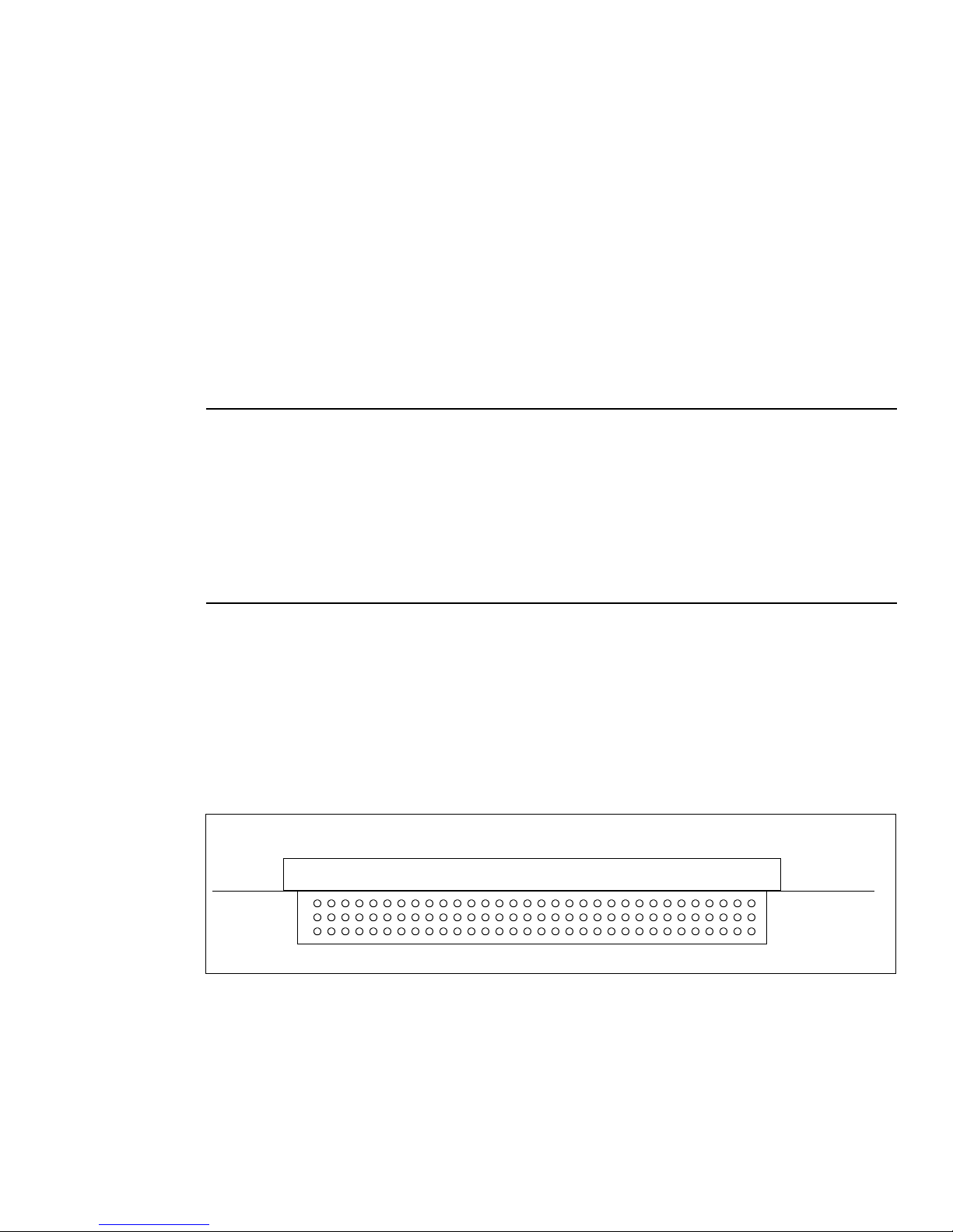
Themis Computer A-1
A
AConnector Pinouts, LEDs, Switches
A.1 Introduction
The following appendix provides the connector pinouts for the user interfaces on the USPIIi-1v as well as
descriptions of other user interfaces such as LEDs and Switches. The baseboard, I/O Board, PMC Carrier
Board, and Paddle Board connector pinouts are each presented as individual sections. For a diagram of the
front panel I/O available on each board, refer to Appendix C, "Front Panel Diagrams."
A.2 Baseboard Front Panel
For a diagram of the baseboard front panel, refer to Appendix C.2, "Baseboard Front Panel."
A.2.1 Baseboard VME P1
• Connector Type: VME32
.
Figure A-1. VME P1 Baseboard Connector Orientation
132
Row A
Row B
Row C
(Top View)
PCB Edge

USPIIi-1v Hardware Manual
A-2
Themis Computer
Table A-1. Baseboard VME P1 Pinout
Pin
Row A
Signal Name
Row B
Signal Name
Row C
Signal Name
1 VME D00 VME BBSY VME D08
2 VME D01 VME BCLR VME D09
3 VME D02 VME ACFAIL VME D10
4 VME D03 VME BGIN0 VME D11
5 VME D04 VME BGOUT0 VME D12
6 VME D05 VME BGIN1 VME D13
7 VME D06 VME BGOUT1 VME D14
8 VME D07 VME BGIN2 VME D15
9 GND VME BGOUT2 GND
10 VME SYSCLK VME BGIN3 VME SYSFAIL
11 GND VME BGOUT3 VME BERR
12 VME DS1 VME BR0 VME SYSRESET
13 VME DS0 VME BR1 VME WORD
14 VME WRITE VME BR2 VME AM5
15 GND VME BR3 VME A23
16 VME DTACK VME AM0 VME A22
17 GND VME AM1 VME A21
18 VME AS VME AM2 VME A20
19 GND VME AM3 VME A19
20 VME IACK GND VME A18
21 VME IACKIN Not Connected VME A17
22 VME IACKOUT Not Connected VME A16
23 VME AM04 GND VME A15
24 VME A07 VME IRQ7 VME A14
25 VME A06 VME IRQ6 VME A13
26 VME A05 VME IRQ5 VME A12
27 VME A04 VME IRQ4 VME A11
28 VME A03 VME IRQ3 VME A10
29 VME A02 VME IRQ2 VME A09
30 VME A01 VME IRQ1 VME A08
31 -12V Not Connected +12V
32 VCC VCC VCC
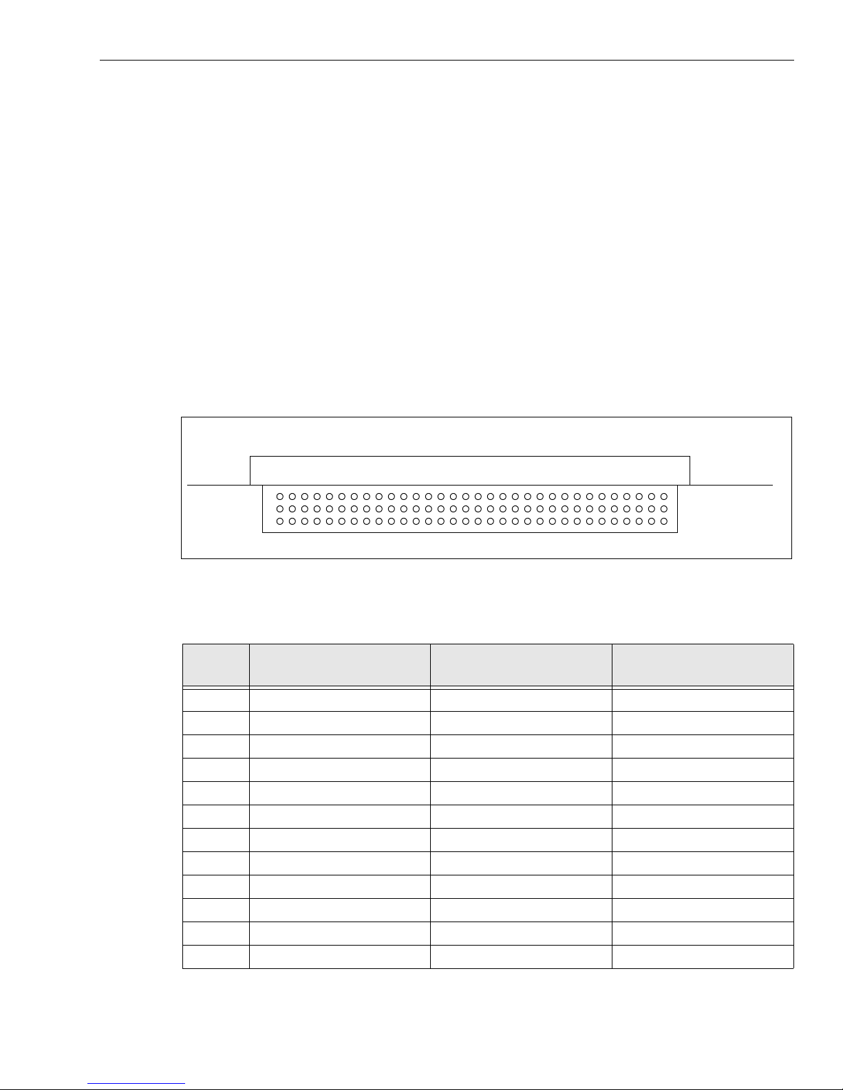
Themis Computer A-3
A. Connector Pinouts, LEDs, Switches
A.2.2 Baseboard VME P2
SCSI port A, Ethernet MII port A and alarm signals are routed to P2. Additional P2 pinout varies with the
board configuration: in PS/2 mode, either PS/2 keyboard/mouse signals or serial port B signals are available
on P2. In Sun mode, Sun keyboard/mouse signals are available on P2. Refer to Section 2.1, "Determine Board
Type and Configuration," on page 2-1. Selection between serial port B and PS/2 keyboard/mouse signals is
made by solder beads SB1801 to SB1811. Refer to Section B.3.1, "Baseboard Solder Beads," on page B-6.
P2 also contains 3 unbuffered, active low, alarm output signals:
– POWER FAIL: Asserted on Power Failure (refer to 6.1.4, "Power Management System," on page
6-3) or when VME ACFAIL is active
– HI TEMP: Asserted when Critical Temperature is reached (refer to 6.2, "Temperature Sensor," on
page 6-5)
– SW ALARM: User-defined. Asserted on a write access to address 0x1ff.f110.0000. Refer to the
USPIIi-1v Software Manual.
• Connector Type: VME32
Figure A-2. Baseboard VME P2 Connector Orientation
Table A-2. Baseboard VME P2 Connector in PS/2 Mode
Pin
Row A
Signal Name
Row B
Signal Name
Row C
Signal Name
1 VCC VCC VCC
2 MII A MDIO GND SCSI A P2
a
3 MII A MDC SCSI A TERMPWR
b
SCSI A TERMPWR
4 MII A RXD3 VME A24 SCSI A ATN
5 MII A RXD2 VME A25 SCSI A BSY
6 MII A RXD1 VME A26 SCSI A ACK
7 MII A RXD0 VME A27 SCSI A RST
8 MII A RX DV VME A28 SCSI A MSG
9 MII A RX CLK VME A29 SCSI A SEL
10 MII A RX ER VME A30 SCSI A CD
11 MII A TX ER VME A31 SCSI A REQ
12 MII A TX CLK GND SCSI A IO
132
Row A
Row B
Row C
(Top View)
PCB Edge
USPIIi-1v Hardware Manual
A-4
Themis Computer
13 MII A TX EN VCC SCSI A DAT<0>
14 MII A TXD0 VME D16 SCSI A DAT<1>
15 MII A TXD1 VME D17 SCSI A DAT<2>
16 MII A TXD2 VME D18 SCSI A DAT<3>
17 MII A TXD3 VME D19 SCSI A DAT<4>
18 MII A COL VME D20 SCSI A DAT<5>
19 MII A CRS VME D21 SCSI A DAT<6>
20 Serial B TXD or
Do not connect
c
VME D22 SCSI A DAT<7>
21 Serial B RXD or
Do not connect
c
VME D23 SCSI A PAR<0>
22 Serial B CTS or
Do not connect
c
GND SCSI A DAT<8>
23 Serial B RTS or
PS/2 KB Data
c
VME D24 SCSI A DAT<9>
24 Serial B DTR or
PS/2 Mouse Data
c
VME D25 SCSI A DAT<10>
25 Serial B DCD or
PS/2 KB CLK
c
VME D26 SCSI A DAT<11>
26 Serial B DSR or
PS/2 VCC FIL
c
VME D27 SCSI A DAT<12>
27 Serial B RI or
PS/2 MSCLK
c
VME D28 SCSI A DAT<13>
28 HI TEMP VME D29 SCSI A DAT<14>
29 POWER FAIL VME D30 SCSI A DAT<15>
30 SW ALARM VME D31 SCSI A PAR<1>
31 GND GND VCC
32 VCC VCC VCC
a. This is part of the Automatic SCSI termination logic: SCSI A P2 signal will be forced to ground by the mating SCSI connector when
attached. This will disable the active onboard SCSI terminator on the P2 side.
b. VME64 Standard for P2 pin B3 is RETRY.
c. Selection is made by solder beads SB1801-1811
Table A-2. Baseboard VME P2 Connector in PS/2 Mode (Continued)
Pin
Row A
Signal Name
Row B
Signal Name
Row C
Signal Name

Themis Computer A-5
A. Connector Pinouts, LEDs, Switches
Table A-3. Baseboard VME P2 Connector in Sun Mode
Pin
Row A
Signal Name
Row B
Signal Name
Row C
Signal Name
1 VCC VCC VCC
2 MII A MDIO GND SCSI A P2
a
3 MII A MDC SCSI A TERMPWR SCSI A TERMPWR
4 MII A RXD3 VME A24 SCSI A ATN
5 MII A RXD2 VME A25 SCSI A BSY
6 MII A RXD1 VME A26 SCSI A ACK
7 MII A RXD0 VME A27 SCSI A RST
8 MII A RX DV VME A28 SCSI A MSG
9 MII A RX CLK VME A29 SCSI A SEL
10 MII A RX ER VME A30 SCSI A CD
11 MII A TX ER VME A31 SCSI A REQ
12 MII A TX CLK GND SCSI A IO
13 MII A TX EN VCC SCSI A DAT<0>
14 MII A TXD0 VME D16 SCSI A DAT<1>
15 MII A TXD1 VME D17 SCSI A DAT<2>
16 MII A TXD2 VME D18 SCSI A DAT<3>
17 MII A TXD3 VME D19 SCSI A DAT<4>
18 MII A COL VME D20 SCSI A DAT<5>
19 MII A CRS VME D21 SCSI A DAT<6>
20 Sun KB Out VME D22 SCSI A DAT<7>
21 Sun KB In VME D23 SCSI A PAR<0>
22 Sun Mouse In GND SCSI A DAT<8>
23 Do not connect VME D24 SCSI A DAT<9>
24 Do not connect VME D25 SCSI A DAT<10>
25 Do not connect VME D26 SCSI A DAT<11>
26 Sun KB VCC VME D27 SCSI A DAT<12>
27 Do not connect VME D28 SCSI A DAT<13>
28 HI TEMP VME D29 SCSI A DAT<14>
29 POWER FAIL VME D30 SCSI A DAT<15>
30 SW ALARM VME D31 SCSI A PAR<1>
31 GND GND VCC
32 VCC VCC VCC
a. This is part of the Automatic SCSI termination logic: SCSI A P2 signal will be forced to ground by the mating SCSI connector when
attached. This will disable the active onboard SCSI terminator on the P2 side.

USPIIi-1v Hardware Manual
A-6
Themis Computer
A.2.3 SCSI A and B
• Connector Type: Honda Dual SCSI-3 (40 MB/sec) Connector, 68 Pin, 0.8 mm Pitch
• Connector Part Number: HDRA-E68WILDT-SL
Figure A-3. Baseboard SCSI A and B Connector Orientation
Table A-4. Baseboard SCSI A and B Pinout
Pin Signal Name Pin Signal Name
1 GND 35 DAT<12>
2 GND 36 DAT<13>
3 GND 37 DAT<14>
4 GND 38 DAT<15>
5 GND 39 PAR<1>
6 GND 40 DAT<0>
7 GND 41 DAT<1>
8 GND 42 DAT<2>
9 GND 43 DAT<3>
10 GND 44 DAT<4>
11 G ND 45 DAT<5>
12 GND 46 DAT<6>
13 GND 47 DAT<7>
14 GND 48 PAR<0>
15 GND 49 GND
16 GND 50 GND
17 TERMPWR 51 TERMPWR
18 TERMPWR 52 TERMPWR
19 GND 53 NC
20 SCSI FP
a
54 GND
134
3568
SCSI Port B
SCSI Port A
134
68
35
Front View of PCB
(J1101)
(J1102)
Themis Computer A-7
A. Connector Pinouts, LEDs, Switches
21 GND 55 ATN
22 GND 56 GND
23 GND 57 BSY
24 GND 58 ACK
25 GND 59 RST
26 GND 60 MSG
27 GND 61 SEL
28 GND 62 CD
29 GND 63 REQ
30 GND 64 IO
31 GND 65 DAT<8>
32 GND 66 DAT<9>
33 GND 67 DAT<10>
34 GND 68 DAT<11>
a. This is part of the Automatic SCSI termination logic: The SCSI FP signal will be forced to ground by the mating SCSI connector when
attached. This will disable the active onboard SCSI terminator on the front side.
Table A-4. Baseboard SCSI A and B Pinout (Continued)
Pin Signal Name Pin Signal Name

USPIIi-1v Hardware Manual
A-8
Themis Computer
A.2.4 RJ45 Ethernet A Connector
• Connector Type: RJ-45 TPE
Figure A-4. Ethernet A Connector Orientation
Table A-5. RJ45 Ethernet A Pinout
Pin Signal Name
1TXD+
2TXD-
3RXD+
44T_D3P
54T_D3P
6RXD-
74T_D4P
84T_D4P
81
Front View of PCB

Themis Computer A-9
A. Connector Pinouts, LEDs, Switches
A.2.5 Keyboard/Mouse Connector and Serial Port A (PS/2 Mode only)
• Connector Type: Two (2), stacked Mini-DB9
• Part Number: ITT Cannon MDSM-18PE-Z10-VR25
Figure A-5. Baseboard Console and Keyboard/Mouse Connector Orientation (PS/2 Mode)
Table A-6. Baseboard Console and Keyboard/Mouse Pinout (PS/2 Mode)
Pins Keyboard/Mouse Signal Names Pins Serial Port A Signal Names
1 KB DATA 10 DCD
2NC11RXD
3GND12TXD
4 VCC 13 DTR
5 KB CLK 14 GND
6GND15DSR
7 Mouse DATA 16 RTS
8 Mouse CLK 17 CTS
9NC18RI
Serial Port A
PS/2 Keyboard/Mouse
1
5
15
18
Front View of PCB

USPIIi-1v Hardware Manual
A-10
Themis Computer
A.2.6 PS/2 Keyboard/Mouse Split Cable
Figure A-6. PS/2 Keyboard/Mouse Split Cable
Table A-7. PS/2 Keyboard/Mouse Split Cable Pinout
Front Panel Keyboard/
Mouse Connector
Pin Number
Signal Name PS/2 Keyboard Pin
Number
a
a. Pins 2 and 6 of the Keyboard Connector are No Connects.
PS/2 Mouse Pin
Number
b
b. Pins 2 and 6 of the PS/2 Mouse Connector are No Connects.
1 KB DATA Keyboard Pin 1 NC
2 NCNCNC
3 GND Keyboard Pin 3 NC
4 VCC Keyboard Pin 4 Mouse Pin 4
5 KB CLK Keyboard Pin 5 NC
6 GND NC Mouse Pin 3
7 Mouse DATA NC Mouse Pin 1
8 Mouse CLK NC Mouse Pin 5
9 NCNCNC
12
3
4
56
Front Panel
Connector
PS/2 Mouse Connector
PS/2 Keyboard Connector
1
2
3
4
5
6
7
8
9
12
3
4
56

Themis Computer A-11
A. Connector Pinouts, LEDs, Switches
A.2.7 Serial Port A (Console) Adapter Cable (PS/2 Mode only)
Figure A-7. Serial Port Adapter Cable
Table A-8. Serial Port A (Console) Adapter Cable
Front Panel Serial Port A
(Console) Pinout
Signal Name Serial Port A Cable Pinout
a
a. All unlisted pins on the DB25 connector are “No Connect.”
Miniature DB9, DB25
1 DCD 8
2RD2
3TD3
4DTR20
5GND7
6DSR6
7RTS4
8CTS5
9RI22
1
2
3
4
5
6
7
8
9
Miniature DB9 (Male)
1
13
14
25
DB25 (Male)
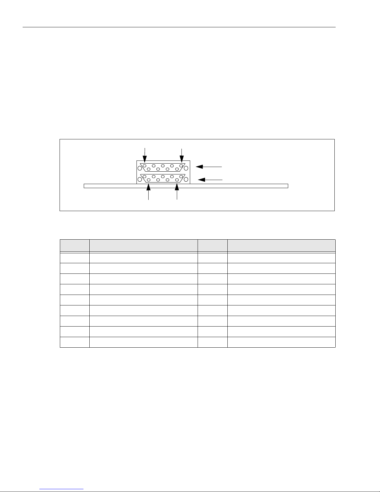
USPIIi-1v Hardware Manual
A-12
Themis Computer
A.2.8 Keyboard/Mouse Connector and Serial Port A (Sun Mode only)
In that configuration, it is possible to connect a SUN type 5 keyboard on the front panel “console” connector,
or on the paddle board #1 DB9 connector. TTYA and TTYB are used to support the SUN Keyboard and
Mouse. Therefore they are no longer available. The console port will be redirected to TTYC (I/O board front
panel). The SUN keyboard/Mouse connects to the front panel console/TTYA port through a cable available
from Themis (Micro SUB DB9 to DIN8. Part Number is 108783)
• Connector Type: Two (2), stacked Mini-DB9
• Part Number: ITT Cannon MDSM-18PE-Z10-VR25
Figure A-8. Baseboard Console and Keyboard/Mouse Connector Orientation (Sun Mode)
Table A-9. Baseboard Console and Keyboard/Mouse Pinout (Sun Mode)
Pins PS/2 Keyboard/Mouse signal names Pins SUN Keyboard/Mouse Signal names
1 DO NOT CONNECT 10 NC
2 NC 11 Sun KB In
3 DO NOT CONNECT 12 Sun KB Out
4 DO NOT CONNECT 13 NC
5 DO NOT CONNECT 14 GND
6 DO NOT CONNECT 15 Sun KB VCC
7 DO NOT CONNECT 16 NC
8 DO NOT CONNECT 17 Sun Mouse In
9NC18NC
Sun Keyboard/Mouse
Do Not Use!
1
5
15
18
Front View of PCB
Themis Computer A-13
A. Connector Pinouts, LEDs, Switches
A.2.9 LEDs
An “ALARM” and a “READY” LED are located on the front panel of the baseboard.
• The “ALARM” LED has three possible colors: green, amber or red. Refer to Chapter 6, "FPGA,
Watchdog, Voltage and Temperature Sensors," for detailed information.
.
• The green “READY” LED is totally controlled by software. Refer to the USPIIi-1v Software Manual
for more information. When OBP takes control of the board at power-on, one of its first instructions is
to turn READY on. If the READY stays off, probably the boot code in Flash is corrupted, or the board
is damaged.
A.2.10 Push-Button RESET
A push button RESET is located on the front panel of the baseboard. This button will initiate a POR Reset to
the UltraSPARC-IIi. This reset is propagated throughout the USPIIi-1v. See Section 7.3.1, "Push Button
Reset," on page 7-3 for details.
Table A-10. Possible colors of the ALARM LED
Color Cause
Green Normal Condition
Amber Cause 1: Level 2 watchdog expired, watchdog is in coping state
Cause 2: Abnormal Power condition, Power Management System in coping state
Cause 3: Board reached Warning Temperature
Red Cause 1: Level 3 watchdog expired, watchdog is in failed state
Cause 2: Abnormal Power condition, Power Management System in failed state
Cause 3: Board reached Critical/Shutdown Temperature

USPIIi-1v Hardware Manual
A-14
Themis Computer
A.3 I/O Board
For a diagram of the I/O Board front panel refer to Appendix C.3, "Baseboard, I/O Board, and Creator
Graphics Front Panels."
Caution —
As VME P1 is not populated, the position occupied by the I/O board (position #2 on USPIIi-1v/
2c and 1v/3) may require jumpering. Refer to Section 2.3, "Backplane Jumper Settings," on page 2-2 for
more information
A.3.1 I/O Board VME P2
SCSI port B, Ethernet MII port B and either serial port C or D are routed to P2. In Sun mode, serial port C
acts as Console Port. Selection between serial port C and D signals on P2 is made by solder beads SB0301 to
SB0306. Refer to Section Figure B-5., "I/O Board Solder Side Solder Beads," on page B-10
• Connector Type: VME32
Figure A-9. I/O Board VME P2 Connector Orientation
Tab l e A - 11 . I/O Board VME P2 Connector
Pin
Row A
Signal Name
Row B
Signal Name
Row C
Signal Name
1 VCC VCC VCC
2 MII B MDIO GND SCSI B P2
a
3 MII B MDC SCSI B TERMPWR SCSI B TERMPWR
4 MII B RXD3 VME A24 SCSI B ATN
5 MII B RXD2 VME A25 SCSI B BSY
6 MII B RXD1 VME A26 SCSI B ACK
7 MII B RXD0 VME A27 SCSI B RST
8 MII B RX DV VME A28 SCSI B MSG
9 MII B RX CLK VME A29 SCSI B SEL
10 MII B RX ER VME A30 SCSI B CD
11 MII B TX ER VME A31 SCSI B REQ
12 MII B TX CLK GND SCSI B IO
132
Row A
Row B
Row C
(Top View)
PCB Edge
Themis Computer A-15
A. Connector Pinouts, LEDs, Switches
13 MII B TX EN VCC SCSI B DAT<0>
14 MII B TXD0 VME D16 SCSI B DAT<1>
15 MII B TXD1 VME D17 SCSI B DAT<2>
16 MII B TXD2 VME D18 SCSI B DAT<3>
17 MII B TXD3 VME D19 SCSI B DAT<4>
18 MII B COL VME D20 SCSI B DAT<5>
19 MII B CRS VME D21 SCSI B DAT<6>
20 Serial C/D TXD VME D22 SCSI B DAT<7>
21 Serial C/D RXD VME D23 SCSI B PAR<0>
22 Serial C/D CTS GND SCSI B DAT<8>
23 Serial C/D RTS VME D24 SCSI B DAT<9>
24 Serial C/D DTR VME D25 SCSI B DAT<10>
25 Serial C/D DCD VME D26 SCSI B DAT<11>
26 Serial C/D DSR VME D27 SCSI B DAT<12>
27 Serial C/D RI VME D28 SCSI B DAT<13>
28 NC VME D29 SCSI B DAT<14>
29 NC VME D30 SCSI B DAT<15>
30 NC VME D31 SCSI B PAR<1>
31 GND GND VCC
32 VCC VCC VCC
a. This is part of the Automatic SCSI termination logic: The SCSI B P2 signal will be forced to ground by the mating SCSI connector when
attached. This will disable the active onboard SCSI terminator on the P2 side.
Table A-11. I/O Board VME P2 Connector
Pin
Row A
Signal Name
Row B
Signal Name
Row C
Signal Name

USPIIi-1v Hardware Manual
A-16
Themis Computer
A.3.2 Serial Port C (TTYC or Console) and Serial Port D (TTYD or Aux Port)
In Sun mode, the two baseboard serial ports (ports A and B) are used by the keyboard and mouse logic,
respectively. Therefore, serial Port C becomes the software console port (also know as TTYA) and serial Port
D is the auxiliary port (TTYB).
In PS/2 mode, all four serial ports are available: ports A and B on the baseboard, port C and D on the I/O
board. Corresponding software acronyms are Console (or TTYA), TTYB, TTYC and TTYD, respectively.
Ports C and D can be configured in RS232 or RS422 mode by means of jumpers JP0705, JP0706, JP0801JP0808. Default setting is RS232. Also, they can be set to synchronous mode by means of jumpers JP0703-
0704. Default is asynchronous. See Appendix Table B-2., "I/O Board Jumper Setting," for details.
Note —
In RS232 mode, only negative signals are used. They are referenced in Appendix Table A-12., "I/
O Board TTY C AND TTY D Pinout," with a minus sign.
• Connector Type: Dual Stacked, 0.050, 26 pin, Sub D, Amplimite Slimline Connector
• Connector Part Number: AMP 786200-1
Figure A-10. I/O Board TTYC and TTYD Connector Orientation
Table A-12. I/O Board TTY C AND TTY D Pinout
Pins TTY C Signal Name Pins TTY D Signal Name
1 CHGND 27 CHGND
2 TXD- 28 TXD-
3RXD-29RXD-
4 RTS- 30 RTS-
5CTS-31CTS-
6NC32NC
7GND33GND
8 DCD- 34 DCD-
9 RXC+ 35 RXC+
10 DCD+ 36 DCD+
52
Front View
of PCB
113
39
TTYC
TTYD

Themis Computer A-17
A. Connector Pinouts, LEDs, Switches
11 T X C+ 37 T X C +
12 NC 38 NC
13 CTS+ 39 CTS+
14 TXD+ 40 TXD+
15 NC 41 NC
16 RXD+ 42 RXD+
17 RXC- 43 RXC-
18 NC 44 NC
19 RTS+ 45 RTS+
20 DTR- 46 DTR-
21 NC 47 NC
22 NC 48 NC
23 DTR+ 49 DTR+
24 TXC- 50 TXC-
25 NC 51 NC
26 NC 52 NC
Table A-12. I/O Board TTY C AND TTY D Pinout
Pins TTY C Signal Name Pins TTY D Signal Name
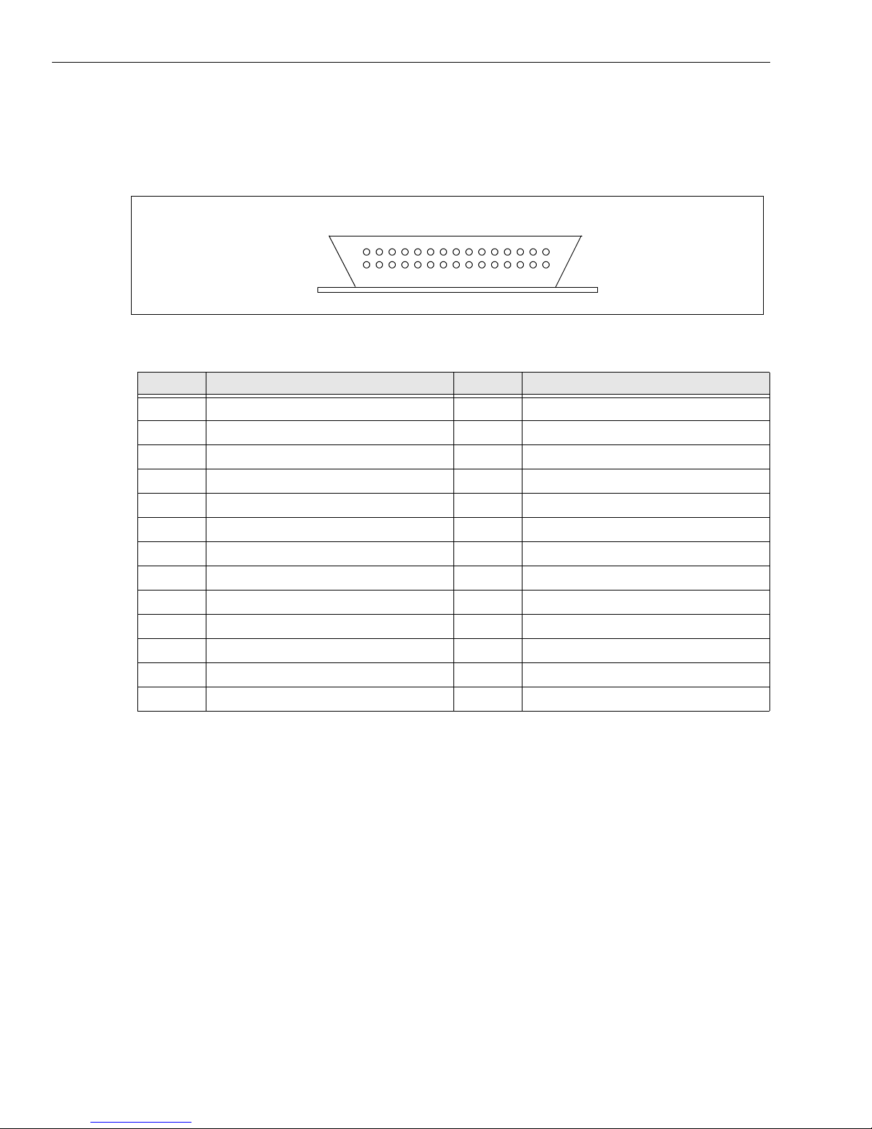
USPIIi-1v Hardware Manual
A-18
Themis Computer
A.3.3 Parallel Port
• Connector Type: 0.050, 26 pin, Sub D, Amplimite Slimline Connector
• Connector Part Number: AMP 750823-1
Figure A-11. I/O Board Parallel Port Connector Orientation
Table A-13. I/O Board Parallel Port Pinout
Pins Signal Name Pins Signal Name
1 ACK 14 STRB
2 BUSY 15 GND
3AFXN16GND
4 INIT 17 GND
5SLCT_IN18 SLCT
6PE19GND
7 ERROR 20 GND
8DAT721GND
9 D AT6 22 DAT5
10 DAT4 23 GND
11 DAT3 24 GND
12 DAT2 25 GND
13 DAT1 26 DAT0
1
13
14
26
Front View
of PCB

Themis Computer A-19
A. Connector Pinouts, LEDs, Switches
A.3.4 RJ45 Ethernet B Connector
• Connector Type: RJ-45 TPE
Figure A-12. Ethernet B Connector Orientation
A.3.5 Audio
A standard miniature audio jack is used for Audio Line-In and Audio Line-out. The part used is the Aston
AT-JY3540-050B.
A.3.6 Creator Graphics Slot
With the USPIIi-1v/2c and 1v/3, a Creator Graphics Card may be installed on the baseboard (UPA64S
connector J4901). The card will occupy the second slot, adjacent to the I/O Board. Video signals are available
on a standard DB13W3 connector. An additional circular DIN connector outputs synchronization signals to
stereo displays.
Table A-14. RJ45 Ethernet B Pinout
Pin Signal Name
1TXD+
2TXD-
3RXD+
44T_D3P
54T_D3P
6RXD-
74T_D4P
84T_D4P
81
Front View of PCB

USPIIi-1v Hardware Manual
A-20
Themis Computer
A.4 PMC Carrier Board
For a diagram of the PMC Board front panel refer to .
A.4.1 PMC Carrier Board P1 Connector
The P1 connector provides daisy-chaining of IACK and BG signals. There is no need to jumper those signals
manually for the position occupied by the PMC carrier.
• Connector Type: VME32
Figure A-13. PMC Carrier Board VME P1 Connector Orientation
Table A-15. PMC Carrier Board VME P1 Pinout
Pin
Row A
Signal Name
Row B
Signal Name
Row C
Signal Name
1NCNCNC
2NCNCNC
3NCNCNC
4 NC DAISY_CHAIN_BG0# NC
5 NC DAISY_CHAIN_BG0# NC
6 NC DAISY_CHAIN_BG1# NC
7 NC DAISY_CHAIN_BG1# NC
8 NC DAISY_CHAIN_BG2# NC
9 GND DAISY_CHAIN_BG2# GND
10 NC DAISY_CHAIN_BG3# NC
11 GND DAISY_CHAIN_BG3# NC
12 NC NC NC
13 NC NC NC
14 NC NC NC
15 GND NC NC
16 NC NC NC
17 GND NC NC
132
Row A
Row B
Row C
(Top View)
PCB Edge
Themis Computer A-21
A. Connector Pinouts, LEDs, Switches
18 NC NC NC
19 GND NC NC
20 NC GND NC
21 DAISY_CHAIN_IACK# NC NC
22 DAISY_CHAIN_IACK# NC NC
23 NC GND NC
24 NC NC NC
25 NC NC NC
26 NC NC NC
27 NC NC NC
28 NC NC NC
29 NC NC NC
30 NC NC NC
31 -12V NC +12V
32 VCC VCC VCC
Table A-15. PMC Carrier Board VME P1 Pinout
Pin
Row A
Signal Name
Row B
Signal Name
Row C
Signal Name
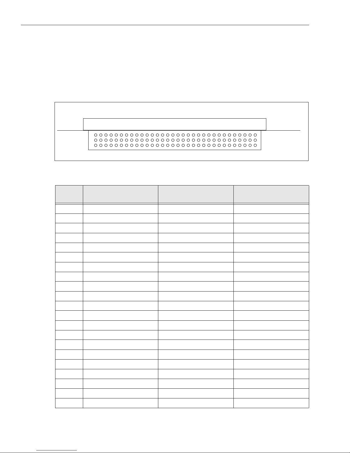
USPIIi-1v Hardware Manual
A-22
Themis Computer
A.4.2 PMC Carrier Board VME P2 Connector
The VME P2 Connector of the PMC Carrier can contain either 64 user-defined signals from PMC slot #1, or
32 signals from PMC slot #1 and 32 from PMC slot #2.
• Connector Type: VME32
Figure A-14. PMC Board VME P2 Connector Orientation
Table A-16. PMC Carrier Board VME P2 Pinout
Pin
Row A
Signal Name
Row B
Signal Name
Row C
Signal Name
1 PMC IO A1 VCC PMC IO C1
2 PMC IO A2 GND PMC IO C2
3 PMC IO A3 NC PMC IO C3
4 PMC IO A4 NC PMC IO C4
5 PMC IO A5 NC PMC IO C5
6 PMC IO A6 NC PMC IO C6
7 PMC IO A7 NC PMC IO C7
8 PMC IO A8 NC PMC IO C8
9 PMC IO A9 NC PMC IO C9
10 PMC IO A10 NC PMC IO C10
11 PMC IO A11 NC PMC IO C11
12 PMC IO A12 GND PMC IO C12
13 PMC IO A13 VCC PMC IO C13
14 PMC IO A14 NC PMC IO C14
15 PMC IO A15 NC PMC IO C15
16 PMC IO A16 NC PMC IO C16
17 PMC IO A17 NC PMC IO C17
18 PMC IO A18 NC PMC IO C18
19 PMC IO A19 NC PMC IO C19
20 PMC IO A20 NC PMC IO C20
21 PMC IO A21 NC PMC IO C21
132
Row A
Row B
Row C
(Top View)
PCB Edge
Themis Computer A-23
A. Connector Pinouts, LEDs, Switches
22 PMC IO A22 GND PMC IO C22
23 PMC IO A23 NC PMC IO C23
24 PMC IO A24 NC PMC IO C24
25 PMC IO A25 NC PMC IO C25
26 PMC IO A26 NC PMC IO C26
27 PMC IO A27 NC PMC IO C27
28 PMC IO A28 NC PMC IO C28
29 PMC IO A29 NC PMC IO C29
30 PMC IO A30 NC PMC IO C30
31 PMC IO A31 GND PMC IO C31
32 PMC IO A32 +5V PMC IO C32
Table A-16. PMC Carrier Board VME P2 Pinout (Continued)
Pin
Row A
Signal Name
Row B
Signal Name
Row C
Signal Name

USPIIi-1v Hardware Manual
A-24
Themis Computer
A.4.3 PMC Carrier Slot User I/O
This section provides the pinout of the 64 PMC User I/O signals that can be brought from PMC cards to the
VME P2 connector of the PMC Carrier board. Also see Appendix A.4.2, "PMC Carrier Board VME P2
Connector," for additional information. Two configurations are possible:
– 64 user signals from PMC slot #1 (connector J5), and none from slot #2. This is the default
configuration.
– 32 user signals from PMC slot #1 (connector J5) and 32 from slot #2 (connector J8). For this
configuration, a special adapter must be installed on connectors J11 and J12. Consult the factory
Both PMC Carrier Slot #1 and Slot #2 use the connector type illustrated in Figure A-15, "PMC Carrier Board
User I/O Connector."
• Connector Type: 64 Pin, Female, 10mm, Dual Row
• Connector Manufacturer: AMP
• Manufacturer’s Part Number: 120528-1
Figure A-15. PMC Carrier Board User I/O Connector
A.4.3.1 PMC Carrier Slot #1: 64 Bit User I/O Configuration
Table A-17. PMC Carrier Slot #1 with 64 Bits of User I/O
Pin Number Signal Pin Number Signal
1 PMC IO C1 33 PMC IO C17
2 PMC IO A1 34 PMC IO A17
3 PMC IO C2 35 PMC IO C18
4 PMC IO A2 36 PMC IO A18
5 PMC IO C3 37 PMC IO C19
6 PMC IO A3 38 PMC IO A19
7 PMC IO C4 39 PMC IO C20
8 PMC IO A4 40 PMC IO A20
9 PMC IO C5 41 PMC IO C21
10 PMC IO A5 42 PMC IO A21
11 PMC IO C6 43 PMC IO C22
12 PMC IO A6 44 PMC IO A22
13 PMC IO C7 45 PMC IO C23
1
2

Themis Computer A-25
A. Connector Pinouts, LEDs, Switches
14 PMC IO A7 46 PMC IO A23
15 PMC IO C8 47 PMC IO C24
16 PMC IO A8 48 PMC IO A24
17 PMC IO C9 49 PMC IO C25
18 PMC IO A9 50 PMC IO A25
19 PMC IO C10 51 PMC IO C26
20 PMC IO A10 52 PMC IO A26
21 PMC IO C11 53 PMC IO C27
22 PMC IO A11 54 PMC IO A27
23 PMC IO C12 55 PMC IO C28
24 PMC IO A12 56 PMC IO A28
25 PMC IO C13 57 PMC IO C29
26 PMC IO A13 58 PMC IO A29
27 PMC IO C14 59 PMC IO C30
28 PMC IO A14 60 PMC IO A30
29 PMC IO C15 61 PMC IO C31
30 PMC IO A15 62 PMC IO A31
31 PMC IO C16 63 PMC IO C32
32 PMC IO A16 64 PMC IO A32
Table A-17. PMC Carrier Slot #1 with 64 Bits of User I/O (Continued)
Pin Number Signal Pin Number Signal

USPIIi-1v Hardware Manual
A-26
Themis Computer
A.4.3.2 PMC Carrier Slot #1: 32 Bit User I/O Configuration
Table A-18. PMC Carrier Slot #1 with 32 Bits of User I/O
Pin Number Signal Pin Number Signal
1 NC 33 PMC IO C17
2 NC 34 PMC IO A17
3 NC 35 PMC IO C18
4 NC 36 PMC IO A18
5 NC 37 PMC IO C19
6 NC 38 PMC IO A19
7 NC 39 PMC IO C20
8 NC 40 PMC IO A20
9 NC 41 PMC IO C21
10 NC 42 PMC IO A21
11 NC 43 PMC IO C22
12 NC 44 PMC IO A22
13 NC 45 PMC IO C23
14 NC 46 PMC IO A23
15 NC 47 PMC IO C24
16 NC 48 PMC IO A24
17 NC 49 PMC IO C25
18 NC 50 PMC IO A25
19 NC 51 PMC IO C26
20 NC 52 PMC IO A26
21 NC 53 PMC IO C27
22 NC 54 PMC IO A27
23 NC 55 PMC IO C28
24 NC 56 PMC IO A28
25 NC 57 PMC IO C29
26 NC 58 PMC IO A29
27 NC 59 PMC IO C30
28 NC 60 PMC IO A30
29 NC 61 PMC IO C31
30 NC 62 PMC IO A31
31 NC 63 PMC IO C32
32 NC 64 PMC IO A32

Themis Computer A-27
A. Connector Pinouts, LEDs, Switches
A.4.3.3 PMC Carrier Slot #2: 32 Bit User I/O Configuration
Table A-19. PMC Carrier Slot #2 with 32 Bits of User I/O
Pin Number Signal Pin Number Signal
1 PMC IO C1 33 NC
2PMC IO A134 NC
3 PMC IO C2 35 NC
4PMC IO A236 NC
5 PMC IO C3 37 NC
6PMC IO A338 NC
7 PMC IO C4 39 NC
8PMC IO A440 NC
9 PMC IO C5 41 NC
10 PMC IO A5 42 NC
11 PMC IO C6 43 NC
12 PMC IO A6 44 NC
13 PMC IO C7 45 NC
14 PMC IO A7 46 NC
15 PMC IO C8 47 NC
16 PMC IO A8 48 NC
17 PMC IO C9 49 NC
18 PMC IO A9 50 NC
19 PMC IO C10 51 NC
20 PMC IO A10 52 NC
21 PMC IO C11 53 NC
22 PMC IO A11 54 NC
23 PMC IO C12 55 NC
24 PMC IO A12 56 NC
25 PMC IO C13 57 NC
26 PMC IO A13 58 NC
27 PMC IO C14 59 NC
28 PMC IO A14 60 NC
29 PMC IO C15 61 NC
30 PMC IO A15 62 NC
31 PMC IO C16 63 NC
32 PMC IO A16 64 NC

USPIIi-1v Hardware Manual
A-28
Themis Computer
A.5 Paddle Board
A.5.1 SCSI Connector
• Connector Type: 68 Pin, Female, Shielded Subminature-D
• Connector Part Number: AMP 787082-7
Figure A-16. Paddle Board SCSI Connector
Table A-20. Paddle Board SCSI Connector Pinout
Pin Signal Name Pin Signal Name
1 GND 35 DAT12
2 GND 36 DAT13
3 GND 37 DAT14
4 GND 38 DAT15
5 GND 39 PAR1
6GND40DAT0
7GND41DAT1
8GND42DAT2
9GND43DAT3
10 GND 44 DAT4
11 G ND 4 5 D AT5
12 GND 46 DAT6
13 GND 47 DAT7
14 GND 48 PAR0
15 GND 49 GND
16 GND 50 NC
17 TERMPWR 51 TERMPWR
18 TERMPWR 52 TERMPWR
19 NC 53 NC
1
68
35
34
Front View
of PCB

Themis Computer A-29
A. Connector Pinouts, LEDs, Switches
20 SCSI P2
a
54 GND
21 GND 55 ATN
22 GND 56 GND
23 GND 57 BSY
24 GND 58 ACK
25 GND 59 RESET
26 GND 60 MSG
27 GND 61 SEL
28 GND 62 CD
29 GND 63 REQ
30 GND 64 IO
31 GND 65 DAT8
32 GND 66 DAT9
33 GND 67 DAT10
34 GND 68 DAT11
a. This is part of the Automatic SCSI termination logic: SCSI P2 signal will be forced to ground by the mating SCSI connector when attached.
This will disable the active onboard SCSI terminator on the P2 side.
Table A-20. Paddle Board SCSI Connector Pinout (Continued)
Pin Signal Name Pin Signal Name
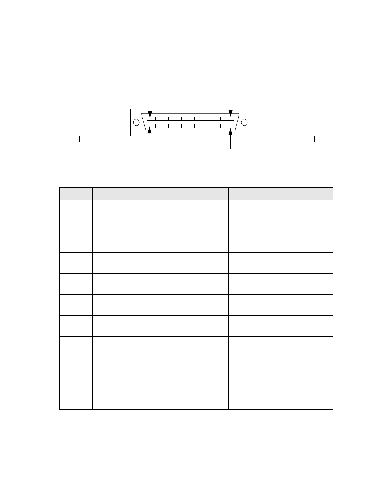
USPIIi-1v Hardware Manual
A-30
Themis Computer
A.5.2 MII Connector
• Connector Type: 40 Pin, Female, Subminiature-D
• Connector Part Number: AMP 787170-4
Figure A-17. Paddle Board MII Connector
Table A-21. Paddle Board MII Connector Pinout
Pin Signal Name Pin Signal Name
1VCC21VCC
2MII_MDIO22 GND
3 MII_MDC 23 GND
4 MII_RXD3 24 GND
5 MII_RXD2 25 GND
6 MII_RXD1 26 GND
7 MII_RXD0 27 GND
8 MII_RX_DV 28 GND
9MII_RX_CLK29 GND
10 MII_RX_ER 30 GND
11 MII_TX_ER 31 GN D
12 MII_TX_CLK 32 GND
13 MII_TX_EN 33 GND
14 MII_TXD0 34 GND
15 MII_TXD1 35 GND
16 MII_TXD2 36 GND
17 MII_TXD3 37 GND
18 MII_COL 38 GND
19 MII_CRS 39 GND
20 MII_POWER 40 MII_POWER
1
40
21
20
Front View of PCB
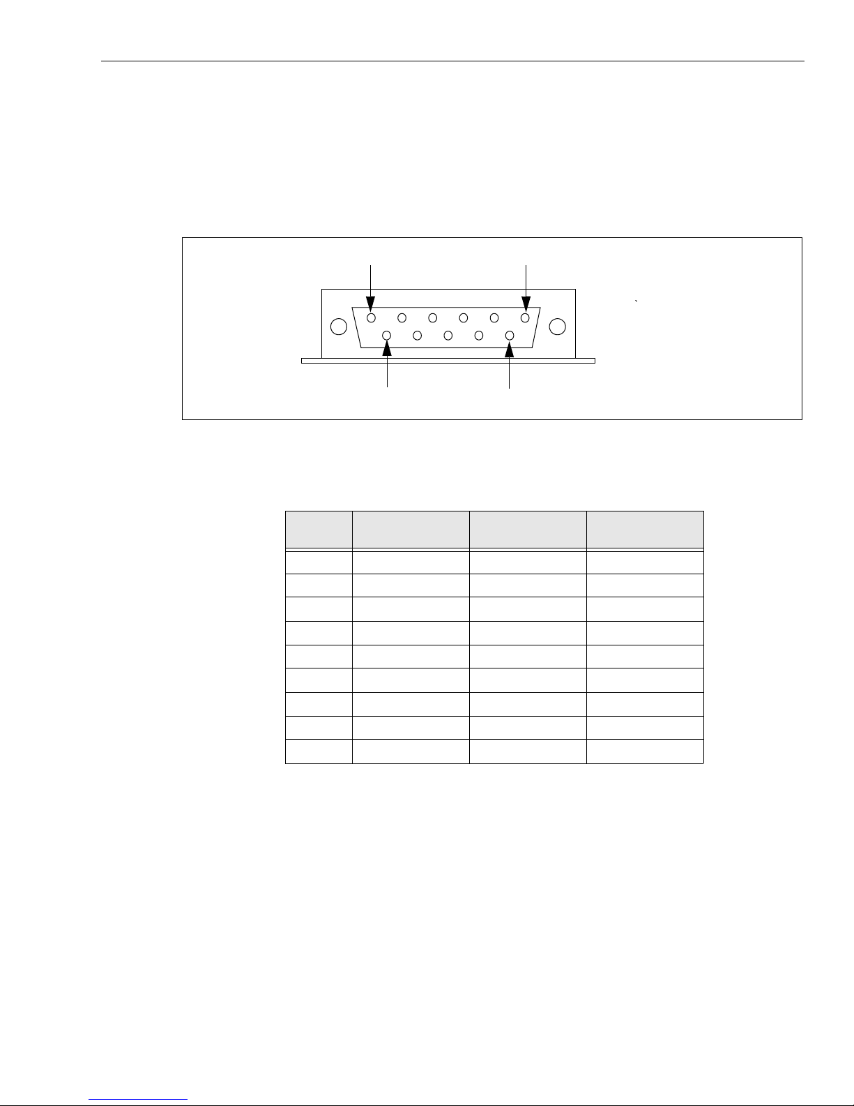
Themis Computer A-31
A. Connector Pinouts, LEDs, Switches
A.5.3 DB9 Connector
The exact signals available on the paddle board DB9 connector vary with the board configuration, as
described in Table 2-1, "Summary of different connectors configuration.," on page 2-4.
• Connector Type: Male, Right Angel, DB9
• Connector Part Number: AMP 747840-4
Figure A-18. Paddle Board DB9 Connector
Table A-22. Paddle Board DB9 Connector Pinout
Pin
Signal name
in serial mode
Signal name
in PS/2 mode
Signal name
in Sun mode
1 DCD KB CLK do not connect
2 RXD do not connect KB IN
3 TXD do not connect KB OUT
4 DTR MOUSE DATA do not connect
5 GND GND GND
6 DSR VCC VCC
7 RTS KB DATA do not connect
8 CTS do not connect MOUSE IN
9 RI MOUSE CLK do not connect
Front View
of PCB
1 5
6
9

USPIIi-1v Hardware Manual
A-32
Themis Computer
 Loading...