

THAT Corporation THAT4311 Datasheet
THAT Corporation
Low-voltage, Low-power
Analog Engine
®
Dynamics Processor
THAT 4311
FEATURES
High Performance VCA, RMS-Level
·
Detector, and three 0pamps in one
package
Wide Dynamic Range: >105 dB
·
Low THD: <0.09%
·
Low Power: 7 mA typ.
·
Surface-Mount Package
·
5 VDC Operation
·
Description
The THAT 4311 Low Power Dynamics Proces
sor combines in a single IC all the active circuitry
needed to construct a wide range of dynamics
processors. The 4311 includes a high performance, voltage controlled amplifier, a log responding RMS-level sensor and three opamps,
one of which is dedicated to the VCA, while the
other two may be used for the signal path or control voltage processing.
The exponentially-controlled VCA provides
two opposing-polarity, voltage sensitive control
ports. Dynamic range exceeds 105 dB, and THD
is typically 0.09% at 0dB gain. The RMS detector
provides accurate RMS to DC conversion over an
APPLICATIONS
Wireless microphone systems
·
Wireless in-ear monitors
·
Compressors and Limiters
·
Gates
·
De-Essers
·
Duckers
·
-
80 dB dynamic range.
Though originally designed for use in micro
phone noise reduction systems, the 4311 is a use
ful building block in a number of analog signal
processing applications. The combination of exponential VCA gain control and logarithmic detector response - “decibel-linear” response simplifies the mathematics of designing the control paths of dynamics processors, making it easy
to develop audio compressors, limiters, gates, expanders, de-essers, duckers, and the like. The
high level of integration ensures excellent temperature tracking between the VCA and the detector,
while minimizing the external parts count.
-
-
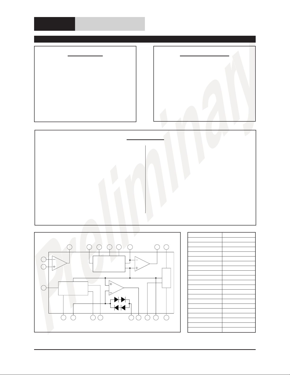
Pin Name DMP20
RMS IN 1
)2
IT (I
18
19
OA1
20
17
16 15
EC-
IN
THAT4311
1
IN
RMS
IT
2
CT
OUT
3
5
4
14 13 12
SYM
EC+
OUT
VCA
OA2
11
VCC
OA3
VREF
VREF
VEE
6
7
9
8
10
Figure 1. THAT 4311 equivalent block diagram
TIME
OA2 -IN 3
RMS OUT 4
)5
CT (C
TIME
CLIP 6
OA2 OUT 7
CAP 8
VREF 9
VEE 10
VCC 11
OA3 OUT 12
VCA OUT 13
SYM 14
EC+ 15
EC- 16
VCA IN 17
OA1 OUT 18
OA1 -IN 19
OA1 +IN 20
Table 1. THAT 4311 pin assignments
THAT Corporation; 45 Sumner Street; Milford, Massachusetts 01757-1656; USA
Tel: +1 508 478 9200; Fax: +1 508 478 0990; Web: www.thatcorp.com

Page 2 Low-voltage, Analog Engine
Preliminary Information
®
Dynamics Processor
SPECIFICATIONS
1
Absolute Maximum Ratings (TA= 25°C)
Positive Supply Voltage (VCC) +15 V Power Dissipation (PD)(TA= 75°C) 700 mW
Operating Temperature Range (T
Max DE
-(EC-) ± 1V
CEC+
) -20 to +70°C Storage Temperature Range (TST) -40 to +125°C
OP
Recommended Operating Conditions
Parameter Symbol Conditions Min Typ Max Units
Positive Supply Voltage V
CC
Electrical Characteristics
Parameter Symbol Conditions Min Typ Max Units
Supply Current I
Reference Voltage V
CC
REF
No signal; VCC=+7 VDC — 7.0 9.0 mA
+5 +15 V
2
1.8 1.95 2.1 V
Encode and Decode – Companding Noise Reduction (VCC= +7V encoder, +15V decoder)
Encode Level Match LMe Encode mode; f = 1kHz -25.3 -23.0 -20.7 dBV
Encode Gain Accuracy Encode mode, f = 1kHz
Decode Level Match LMd Decode mode; f = 1kHz -18.3 -16.0 -13.7 dB
Decode Gain Accuracy Decode mode; f=1kHz
Max Input Voltage Vime Encode mode; THD = 3%; f = 1kHz 3 5 — dBV
Max Output Voltage Vomd Decode mode; THD = 3%; f = 1kHz 10.7 13.7 — dBV
Total Harmonic Distortion THDtrim End-to-end; Vin = LMe; f = 1kHz — 0.025 — %
(with trim)
Total Harmonic Distortion THDnotrim End-to-end; Vin = LMd; f = 1kHz — 0.15 0.7 %
(no trim)
Output Noise Vnod End-to-end ; Vin = short; A-weighted — 7 — µVrms
GAe1 Vin = LMe + 10dB +3.5 +5 +6.5 dB
GAe2 Vin = LMe - 40dB -23 -20 -17 dB
GAd1 Vin = LMd + 5dB +8.5 +10 +11.5 dB
GAd2 Vin = LMd - 20dB -43 -40 -37 dB
1. All specifications are subject to change without notice.
2. Unless otherwise noted, T
=25°C, test circuit as shown in Fig 2.
A
THAT Corporation; 45 Sumner Street; Milford, Massachusetts 01757-1656; USA
Tel: +1 508 478 9200; Fax: +1 508 478 0990; Web: www.thatcorp.com
Rev. 08/30/01 Page 3
Preliminary Information
Electrical Characteristics (con’t)
Parameter Symbol Conditions Min Typ Max Units
Op amp OA1
Offset Voltage V
Equivalent Input Noise V
nOA1
Total Harmonic Distortion THD
Open Loop Gain A
VO-OA1
Gain Bandwidth Product GBW
Slew Rate SR
Op amp OA2
Offset Voltage V
Equivalent Input Noise V
Total Harmonic Distortion THD
Open Loop Gain A
Gain Bandwidth Product GBW
Slew Rate SR
nOA1
VO-OA1
IO
OA1
IO
OA1
OA1
OA1
OA1
OA1
RL=2kW — ±0.5 ±6 mV
A-weighted 6.5 10
nV
1kHz, AV=1; RL= 10kW — 0.0007 0.003 %
RL= 10kW--115 --
at 50kHz — 5 —
—2—
RL=2kW — ±0.5 ±6 mV
A-weighted 7.5 12
nV
1kHz, AV=1; RL= 10kW — 0.0007 0.003 %
RL= 10kW--110 --
at 50kHz — 5 —
—2—
Hz
Hz
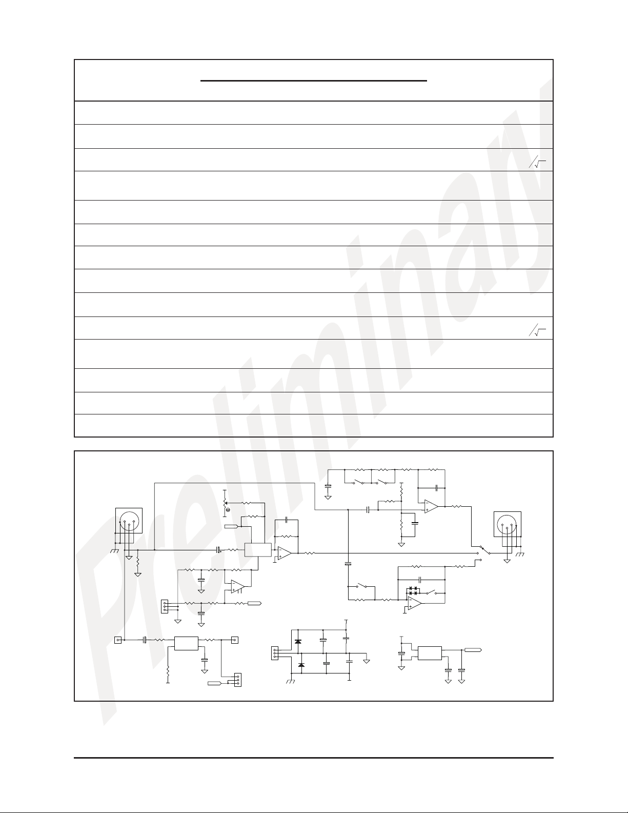
Input
XLR1
XLR-F
2
5
4
TP1
RMS Input
+40dB +60dB
+20dB
+
R10
100R 5%
Bypass
Capacitors
D3
1N4004
D4
1N4004
C15
1000u
+
0dB
V+
+
C10
22u
+
C13
22u
V+
Sym
1
3
3
1
2
R1
100k
External
Control
Input
C6
+
47u
R11
23k2
3
2
1
CN1
Iset2TC
THAT4311
R12
261k
V-
R2
10k0
R21
10k0
U1B
IN1OUT
RMS
R3
10k0
C12
3u3
R20
10k0
C9
3u3
R26
4
5
100R
5%
+
C7
10u
VREF
50k
R7
C4
47u
R8
cw
300k
V-
VREF
R5
17
20k0
R4
1k33
2
3
81
R29
1k33
TP2
RMS Output
RMS Output
3
2
1
CN1
5%
R9
51R
5%
1415
EC+ SYM
OUT
IN
EC-
16
VCA
VREF
CONTROL-VOLTAGE
6
U1
OP-27
VREF
Power
Input
3
2
1
CN2
13
C5
47p
R6
20k0
U1A
OA3
THAT4311
NPO
12
C11
100n
(U1)
V-
R24
2k80
SW1F
C19
1000u
SW1C
16
R15
31k6
C14
100n
(U1)
611
C16
47u
R23
280R
512
SW1E
R19
100k
+
R18
10k0
1
+40dB
R16
280R
C1
10u
R22
30R1
V+
10k0
3
VREF
V+
+
R27
19
20
+
C18
47u
R17
31k6
C8
OA2
U1C
THAT4311
U1E
11
VCC
VEE
10
THAT4311
R14
31k6
OA1
U1D
THAT4311
47p
SW1B
2
6
7
VREF
C17
47p
VREF
CAP
15
10u
Output
SW1A
XLR2
XLR-M
1
3
3
1
2
5
2
4
R25
18
100R
5%
R28
100R 5%
VREF
9
8
+
+
C3
C2
22u
Fig 2. THAT 4311 test circuit
THAT Corporation; 45 Sumner Street; Milford, Massachusetts 01757-1656; USA
Tel: +1 508 478 9200; Fax: +1 508 478 0990; Web: www.thatcorp.com
Page 4 Low-voltage Analog Engine
Preliminary Information
Representative Data (Stand-alone)
®
Dynamics Processor
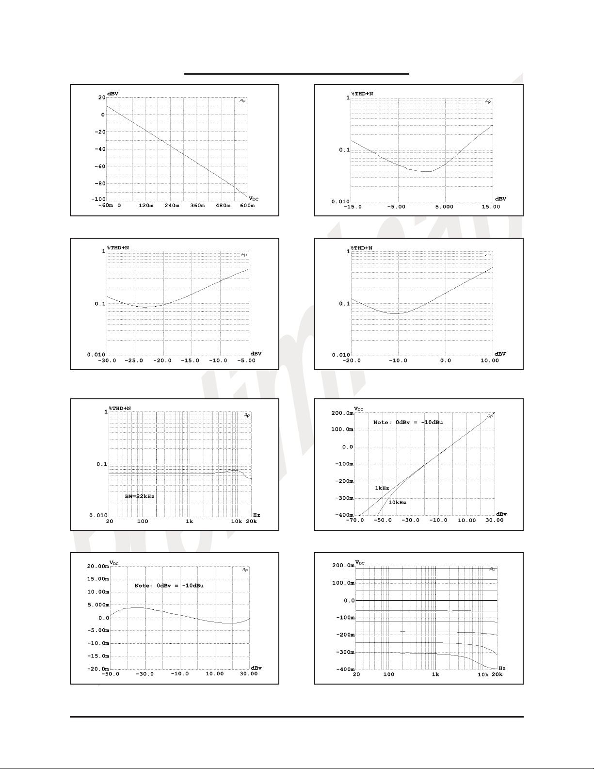
Fig 3. VCA Gain vs. Control Voltage (Ec-) at 25°C
Fig 5. VCA 1kHz THD+Noise vs. Input, +15 dB Gain Fig 6. VCA 1kHz THD+Noise vs. Input, 0 dB Gain
Fig 4. VCA 1kHz THD+Noise vs. Input, -15 dB Gain
Fig 7. VCA THD vs. Frequency, 0 dB gain, 1 Vrms Input
Fig 9. Departure from Ideal Detector Law vs. Level
THAT Corporation; 45 Sumner Street; Milford, Massachusetts 01757-1656; USA
Tel: +1 508 478 9200; Fax: +1 508 478 0990; Web: www.thatcorp.com
Fig 8. RMS Output vs. Input Level, 1 kHz & 10 kHz
Fig 10. Detector Output vs. Frequency at Various Levels
 Loading...