

THAT Corporation THAT4301S, THAT4301P Datasheet
THAT Corporation; 45 Sumner Street; Milford, Massachusetts 01757-1656; USA
Tel: +1 (508) 478-9200; Fax: +1 (508) 478-0990; Web: www.thatcorp.com
THAT Corporation
THAT Analog Engine
®
IC Dynamics Processor
THAT 4301, 4301A
FEATURES
·
High-Performance Voltage
Controlled Amplifier
·
High-Performance RMS-Level
Detector
·
Three General-Purpose Opamps
·
Wide Dynamic Range: >115 dB
·
Low THD: <0.03%
·
Low Cost: $4.39 (‘000s)
·
DIP & Surface-Mount Packages
APPLICATIONS
·
Compressors
·
Limiters
·
Gates
·
Expanders
·
De-Essers
·
Duckers
·
Noise Reduction Systems
·
Wide-Range Level Meters
Description
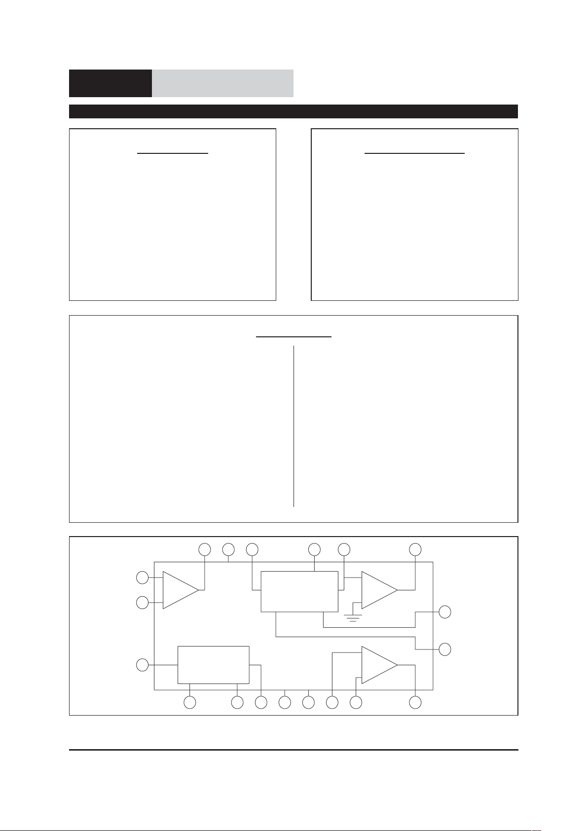
THAT 4301 Dynamics Processor, dubbed
“THAT Analog Engine,” combines in a single IC
all the active circuitry needed to construct a
wide range of dynamics processors. The 4301
includes a high-performance, exponentially-controlled VCA, a log-responding
RMS-level sensor and three general- purpose
opamps.
The VCA provides two opposing-polarity, voltage-sensitive control ports. Dynamic range exceeds 115 dB, and THD is typically 0.003% at 0
dB gain. In the 4301A, the VCA is selected for
low THD at extremely high levels. The RMS de
tector provides accurate rms-to-dc conversion
over an 80 dB dynamic range for signals with
crest factors up to 10. One opamp is dedicated
as a current-to-voltage converter for the VCA,
while the other two may be used for the signal
path or control voltage processing.
The combination of exponential VCA gain control and logarithmic detector response — “decibel-linear” response — simplifies the
mathematics of designing the control paths of
dynamics processors. This makes it easy to design audio compressors, limiters, gates, expanders, de-essers, duckers, noise reduction
systems and the like. The high level of integra
-
tion ensures excellent temperature tracking be
tween the VCA and the detector, while
minimizing the external parts count.
OUT
CTIT
IN
-
+
-
1
18
11
17
14
13
12
15
16
19
20
2
5
4
9
10 8
6
7
-
OA1
+
VCC
THAT4301
EC-
EC+
IN
OUT
SYM
VCA
OA3
+
OA2
GND
VEE
RMS
Figure 1. Block Diagram (pin numbers are for DIP only)
THAT Corporation; 45 Sumner Street; Milford, Massachusetts 01757-1656; USA
Tel: +1 (508) 478-9200; Fax: +1 (508) 478-0990; Web: www.thatcorp.com
Page 2 Rev. 04/10/02
SPECIFICATIONS
1,2
Absolute Maximum Ratings (TA= 25°C)
Positive Supply Voltage (VCC) +18 V
Negative Supply Voltage (V
EE
) -18 V
Supply Current (I
CC
)20mA
Power Dissipation (P
D
)(TA= 75°C) 700 mW
Operating Temperature Range (T
OP
) 0 to +70°C
Storage Temperature Range (T
ST
) -40 to +125°C
Overall Electrical Characteristics
Parameter Symbol Conditions Min Typ Max Units
Positive Supply Voltage V
CC
+7 — +15 V
Negative Supply Voltage V
EE
-7 — -15 V
Positive Supply Current I
CC
—1218 mA
Negative Supply Current I
EE
— -12 -18 mA
Thermal Resistance q
J-C
SO-Package — 140 — °C/W
VCA Electrical Characteristics
3
4301 4301A
Parameter Symbol Conditions Min Typ Max Min Typ Max Units
Input Bias Current I
B(VCA)
No Signal — 30 400 — 30 400 pA
Input Offset Voltage V
OFF(VCA In)
No Signal — ±4 ±15 — ±4 ±15 mV
Input Signal Current I
IN(VCA)
or I
OUT(VCA)
— 175 750 — 175 750 mArms
Gain at 0V Control G
0
EC+=EC–= 0.000V -0.4 0.0 +0.4 -0.4 0.0 +0.4 dB
Gain-Control Constant T
A
= 25°C (T
CHIP
@ 55°C)
-60 dB < gain < +40dB
E
C+
/Gain (dB) EC+& SYM 6.4 6.5 6.6 6.4 6.5 6.6 mV/dB
EC-/Gain (dB) E
C-
-6.4 -6.5 -6.6 -6.4 -6.5 -6.6 mV/dB
Gain-Control TempCo DEC/ DT
CHIP
Ref T
CHIP
= 27°C — +0.33 — — +0.33 — %/°C
Gain-Control Linearity -60 to +40 dB gain — 0.5 2 — 0.5 2 %
Off Isolation EC+=SYM=-375mV, EC-=+375mV 110 115 — 110 115 — dB
Output Offset Voltage Change DV
OFF(OUT)
R
out
= 20kW
0 dB gain — 1 3 — 1 3 mV
+15 dB gain — 2 10 — 2 10 mV
+30 dB gain — 5 25 — 5 25 mV
Gain Cell Idling Current I
IDLE
—20— —20— mA
Output Noise e
n(OUT)
20 Hz-20 kHz
R
out
= 20kW
0 dB gain — -96 -94 — -96 -94 dBV
+15 dB gain — -85 -83 — -85 -83 dBV
Total Harmonic Distortion THD V
IN
= 0 dBV, 1 kHz
0 dB gain — 0.003 0.007 — 0.003 0.007 %
1. All specifications subject to change without notice.
2. Unless otherwise noted, T
A
=25°C, VCC= +15V, VEE= -15V; VCA
SYM
adjusted for min THD@1V,1kHz, 0 dB gain.
3. Test circuit is the VCA section only from Figure 2.
THAT Corporation; 45 Sumner Street; Milford, Massachusetts 01757-1656; USA
Tel: +1 (508) 478-9200; Fax: +1 (508) 478-0990; Web: www.thatcorp.com
THAT 4301 Dynamics Processor IC Page 3
SPECIFICATIONS
1,2
(Cont’d.)
VCA Electrical Characteristics3(Cont’d.)
4301 4301A
Parameter Symbol Conditions Min Typ Max Min Typ Max Units
Total Harmonic Distortion (cont’d.) THD V
IN
= +10 dBV, 1 kHz
0 dB gain — 0.03 0.07 — 0.03 0.07 %
–15 dB gain — 0.035 0.09 — 0.035 0.09 %
V
OUT
= +10 dBV, 1 kHz
+15 dB gain — 0.035 0.09 — 0.035 0.09 %
V
IN
= +19.5 dBV, 1 kHz
0 dB gain — — — — 0.05 0.09 %
Symmetry Control Voltage V
SYM
minimum THD -2.5 0 +2.5 -2.5 0 +2.5 mV
RMS Detector Electrical Characteristics
4
Parameter Symbol Conditions Min Typ Max Units
Input Bias Current I
B (RMS)
No Signal — 30 400 pA
Input Offset Voltage V
OFF(RMS In)
No Signal — ±4 ±15 mV
Input Signal Current I
IN(RMS)
— 175 750 mA
Input Current for 0 V Output I
in0
IT= 7.5mA 6 8.5 12 mA
Output Scale Factor E
O
/ 20log(Iin/I
in0
) 31.6nA< IIN< 1mA
TA= 25°C (T
CHIP
»55°C) 6.4 6.5 6.6 mV/dB
Scale Factor Match (RMS to VCA) -20 dB < VCA Gain < +20 dB
1mA<I
in (DET)
<100mA .985 1 1.015
Output Linearity f
IN
= 1kHz
1mA<I
in
< 100mA — 0.1 — dB
100nA < I
in
< 316mA — 0.5 — dB
31.6nA < Iin< 1mA — 1.5 — dB
Rectifier Balance f
IN
= 100 Hz, t = .001 s
1mA< Iin< 100mA –20 — 20 %
Crest Factor 1ms pulse repetition rate
0.2 dB error — 3.5 —
0.5 dB error — 5 —
1.0 dB error — 10 —
Maximum Frequency for 2 dB Additional Error I
in
³ 10mA — 100 — kHz
I
in
³ 3mA — 45 — kHz
Iin³ 300nA — 7 — kHz
Timing Current Set Range I
T
1.5 7.5 15 mA
Voltage at ITPin IT= 7.5mA -10 +20 +50 mV
Timing Current Accuracy ICT/I
T
IT= 7.5mA 0.90 1.1 1.30
Filtering Time Constant t T
CHIP
=55°C
()0 026.
C
I
T
T
s
Output Temp. Coefficient DEo/ DT
CHIP
Re: T
CHIP
=27°C — 0.33 — %/°C
Output Current I
OUT
–300mV < V
OUT
< +300mV ±90 ±100 — mA
4. Except as noted, test circuit is the RMS-Detector section only from Figure 2.
THAT Corporation; 45 Sumner Street; Milford, Massachusetts 01757-1656; USA
Tel: +1 (508) 478-9200; Fax: +1 (508) 478-0990; Web: www.thatcorp.com
Page 4 Rev. 04/10/02
Specifications
1,2
(Cont’d)
Opamp Electrical Characteristics
5
OA1 OA2 OA3
Parameter Symbol Conditions Min Typ Max Min Typ Max Min Typ Max Units
Input Offset Voltage V
OS
— ±0.5 ±6—±0.5 ±6—±0.5 ±6mV
Input Bias Current I
B
— 150 500 — 150 500 — 150 500 nA
Input Offset Current I
OS
— 15 50 — 15 50 N/A nA
Input Voltage Range I
VR
— ±13.5 — — ±13.5 — N/A V
Common Mode Rej. Ratio CMRR RS<10k — 100 — — 100 — N/A
Power Supply Rej. Ratio PSRR VS=±7V to ±15V — 100 — — 100 — — 100 —
Gain Bandwidth Product GBW (@50kHz) — 5 — — 5 — — 5 — MHz
Open Loop Gain A
VO
RL=10k — 115 — — 110 — — 125 —
RL=2k N/A N/A — 120 —
Output Voltage Swing V
O@RL
=5kW — ±13 — — ±13 — — ±14 — V
VO@RL=2kW N/A N/A — — ±13 — V
Short Circuit Output Current — 4 — — 4 — — 12 — mA
Slew Rate SR — 2 — — 2 — — 2 — V/ms
Total Harmonic Distortion THD 1kHz, A
V
=1, RL=10kW — 0.0007 0.003 — 0.0007 0.003 — 0.0007 0.003 %
1kHz, AV=–1, RL=2kW N/A N/A — 0.0007 0.003 %
Input Noise Voltage Density e
n
fO=1kHz — 6.5 10 — 7.5 12 — 7.5 12
nV Hz
Input Noise Current Density i
n
fO=1kHz — 0.3 — — 0.3 — — 0.3 —
pA Hz
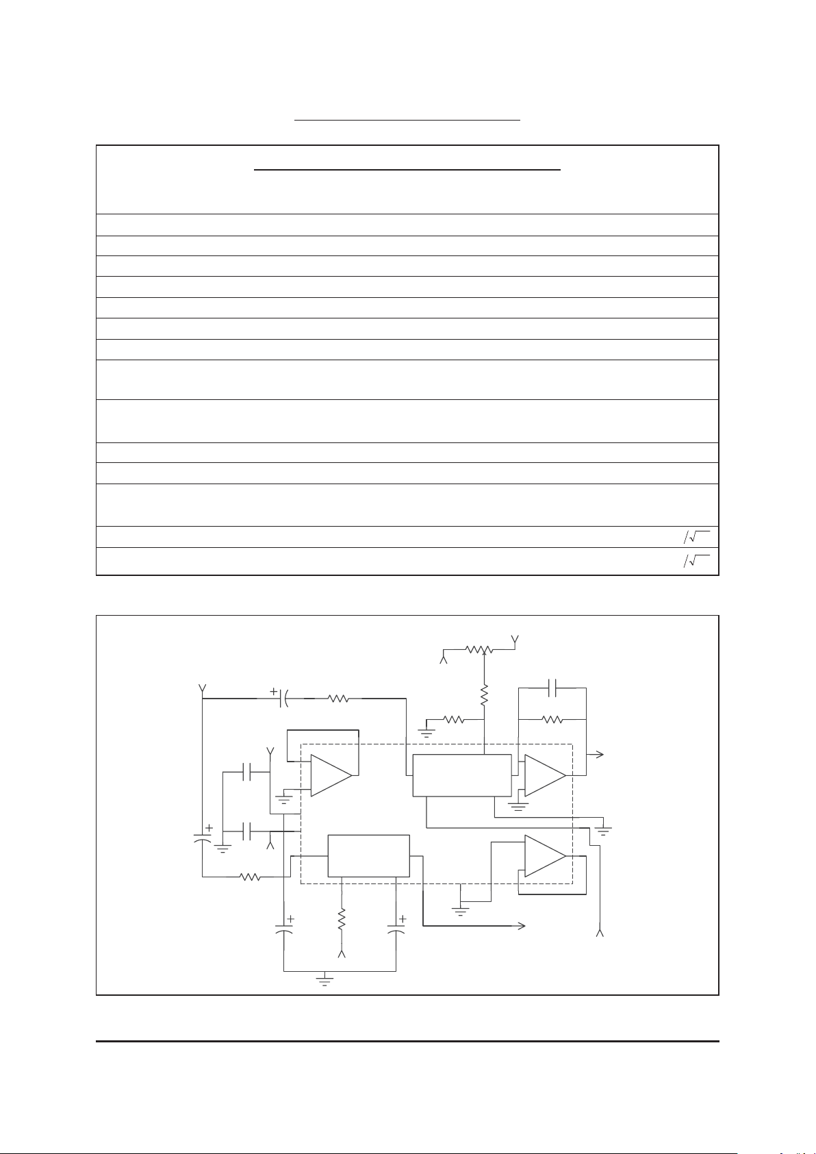
50K
R5
47uF
C1
10uF
C4
22uF
C6
300K
R4
51
R3
1%
R1
1%
R2
47pF
C2
1%
10K0
R6
47uF
C3
1%
2M00
R7
100n
C7
100n
C8
Ct
OA2
OA1
VEE
VCC
GND
-
+
VCA
-
-
+
VCA SYM
IN
SIGNAL
Ec-
OUT
SIGNAL
OUT
RMS
+15V
+15V
-15V
-15V
-15V
20K0
20K0
THAT4301
IN
RMS
It
SYM
OUT
IN
EC-
EC+
OA3
OUT
+
Figure 2. VCA and RMS detector test circuit
5. Test circuit for opamps is a unity-gain follower configuration, with load resistor R
L
as specified.
 Loading...