

THAT Corporation THAT2252 Datasheet
K
THAT Corporation
IC RMS-Level Detector
THAT 2252
FEATURES
True RMS Response
·
Wide Dynamic Range: >80 dB
·
High Crest Factor: 8 (1 dB error)
·
Wide Bandwidth: to > 20 kHz
·
Logarithmic Output Scaling
·
Low Cost: $2.20 in ’000s
·
Single In-Line Package
·
Matches 2180 and 2181 Series
·
VCAs
Description
The THAT 2252 integrated-circuit rms-level detector is designed to convert an ac input current into a
dc output voltage. The output is proportional to the
log of the true rms value of the input signal. The
parts are housed in a space-efficient plastic 8-pin
single-in-line (SIP) package, and require minimal
support circuitry. Based on dbx technology and fab-
APPLICATIONS
Meters
·
Spectrum Analyzers
·
Compressors
·
Expanders
·
Oscillators
·
Psychoacoustic Modeling
·
Noise Measurement
·
ricated in a super low-noise process, the 2252 combines wide dynamic range with frequency response
to beyond 20 kHz. The logarithmic output is especially convenient for audio applications requiring
decibel-linear scaling. The integration time is adjustable via an external R/C pair. With some external circuitry, response to dc is also possible.
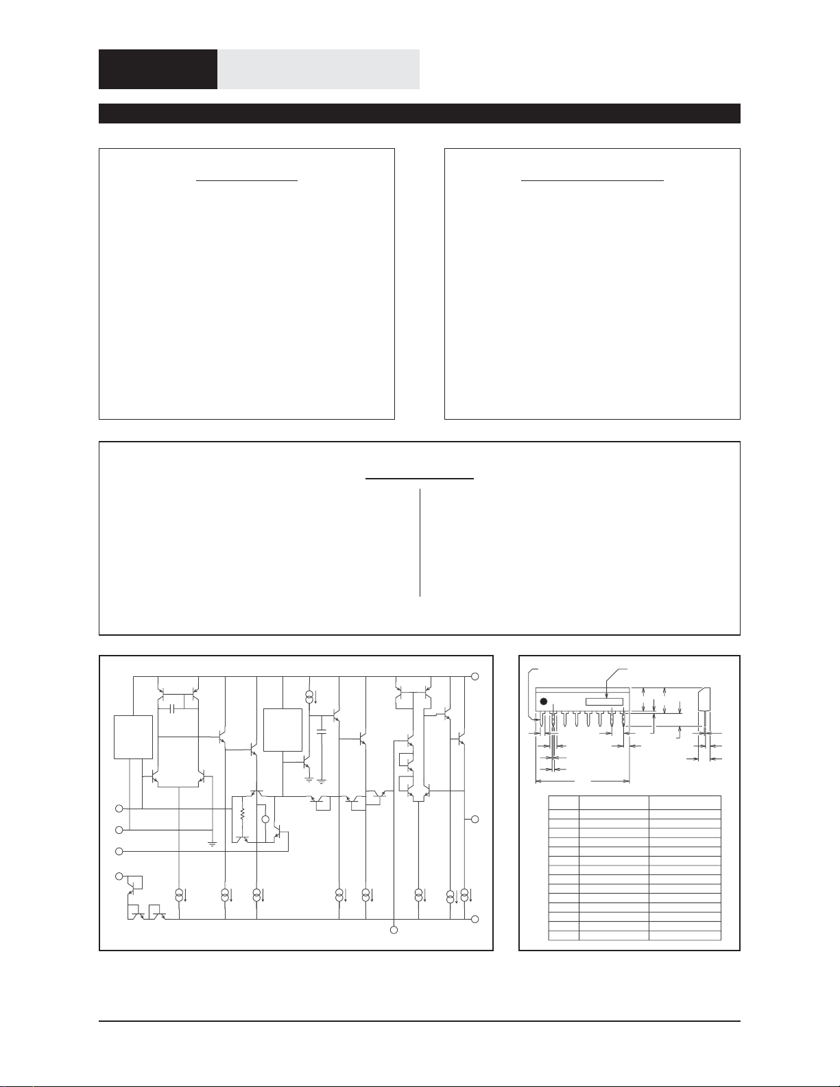
BIAS
CURRENT
COMP
1
1
3
4
2
PIN 1
8
THAT
BIAS
CURRENT
COMP
2
+
V
-
Figure 1. 2252 Equivalent Circuit Diagram
7
5
6
N
B
D
C
ITEM
A 20.32 MAX.
B
C
D
E
F
G
H
I
J
K
L
MN3.2 ± 0.5
Figure 2. 2252 Physical Outline
dbx is a registered trademark of Carillon Electronics Corporation
THAT Corporation; 45 Sumner Street; Milford, Massachusetts 01757-1656; USA
Tel: +1 508 478 9200; Fax: +1 508 478 0990; Web: www.thatcorp.com
MODEL NO.
H
TYP.
A
MILLIMETERS INCHES
1.1 MIN.
0.5 ± 0.1
0.25
2.54
1.27 MAX.
0.51 MIN.
5.08 MAX.
2.8 ± 0.2
5.75 MAX.
1.5 MAX.
0.25 +0.10 -0.04
1.1 MIN.
GE
F
0.8 MAX.
0.043 MIN.
0.02 ± 0.004
0.01
0.1
0.05 MAX.
0.02 MIN.
0.2 MAX.
0.11 ± 0.008
0.227 MAX.
0.058 MAX.
0.01 +0.004 -0.002
0.126 ± 0.02
0.043 MIN.
J
M
L
I
Page 2 THAT 2252 RMS-Level Detector
SPECIFICATIONS
1
Absolute-Maximum Ratings (TA = 25°C)
Positive Supply Voltage (VCC) +18 V
Negative Supply Voltage (VEE) -18 V
Supply Current (ICC) 10 mA
Power Dissipation (PD) 330 mW
Operating Temperature Range (TOP) -20 to +75°C
Storage Temperature Range (TST) -40 to +125°C
Recommended Operating Conditions
Parameter Symbol Conditions Min Typ Max Units
Positive Supply Voltage V
Negative Supply Voltage V
Bias Set Current I
Signal Current I
Timing Current I
CC
EE
BIAS
I
in
T
=24mA— — 1 mA
BIAS
Electrical Characteristics
+4 +12 +15 V
-4 -12 -15 V
15 24 50 mA
1 7.5 50 mA
2
Parameter Symbol Conditions Min Typ Max Units
Supply Current I
Equiv. Input Bias Current I
Input Offset Voltage V
Symmetry Voltage V
CC
B
OFF(IN)
SYM
Output Scale Factor EO/20log(Iin/ I
Input Current for 0V Output I
in0
in0
No Signal — 1 3 mA
No Signal — 5 8 nA
No Signal 0 +8 +16 mV
-2 8 +18 mV
) 31.6nA<IIN<1mA
T
=25°C (T
A
»35°C) 6.0 6.1 6.2 mV/dB
CHIP
II
× II
BIAS T
3.5
×
BIAS T
2.9
II
×
BIAS T
2.4
Output Linearity fIN= 1kHz
1mA<I
100nA < I
31.6nA < I
< 100mA — 0.1 — dB
in
< 316mA — 0.5 — dB
in
< 1mA — 1.0 — dB
in
Crest Factor 1ms pulse repetition rate
0.2 dB error — 3.5 —
0.5 dB error — 5 —
1.0 dB error — 8 —
Maximum Frequency for 1 dB additional error Iin³ 100mA — 80 — kHz
I
³ 10mA 74 — kHz
in
I
³ 1mA 30 — kHz
in
I
³ 100nA 4 — kHz
in
C
Filtering Time Constant
().026
T
I
T
s
Output TempCo D E
0
/ D T
CHIP
Re: T
1. All specifications subject to change without notice.
2. Unless otherwise noted, T
minimum ripple at V
out
=25°C, VCC= +15V, VEE= -15V. Test circuit is as shown in Figure 4. SYM is adjusted for
A
with Vin=1 V
, 100 Hz.
RMS
THAT Corporation; 45 Sumner Street; Milford, Massachusetts 01757-1656; USA
Tel: +1 508 478 9200; Fax: +1 508 478 0990; Web: www.thatcorp.com
=27°C — 0.33 — %/°C
CHIP
600032 Rev 01 Page 3
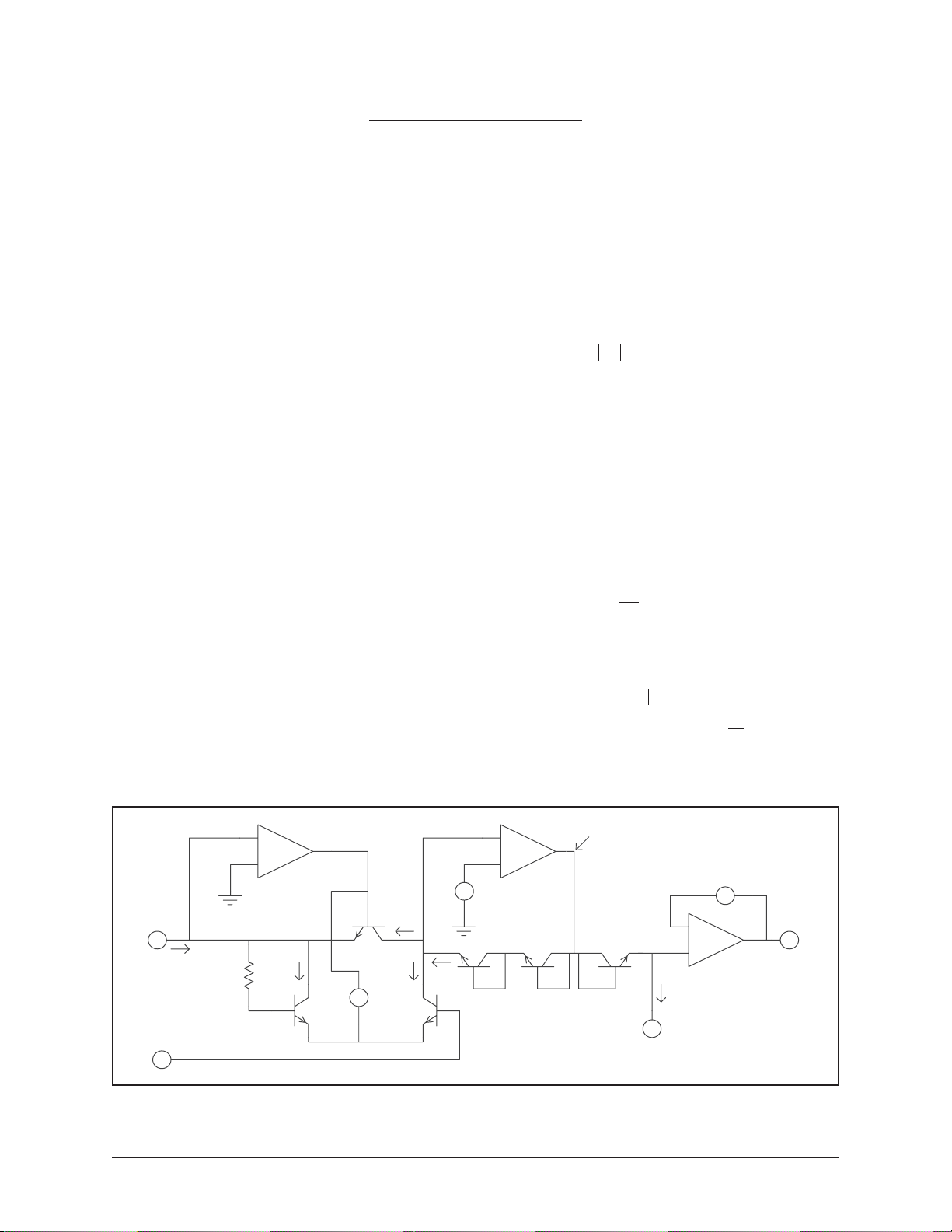
Theory of Operation
The THAT 2252 RMS-Level Detector is designed
for high performance in audio-frequency applica
tions requiring logarithmic output, rms response,
and wide dynamic range. The parts compute rms
level by rectifying input current signals, converting
the resulting current waveform to a logarithmic
voltage, and applying this voltage to a log-domain
filter.
Current Rectification
Figure 3 presents a simplified internal circuit dia
gram of the 2252. The input signal current, I
flows in pin 1, the input pin. OA1 drives the base
of Q3 and the emitter of Q1 (through V1) to main
tain pin 1 at virtual ground potential. A negative
input current (flowing out of pin 1) will tend to
drive the inverting input of OA1 negative, driving
OA1’s output positive, turning on Q3. V1 is de
signed to cut off Q1 while Q3 is on. Therefore, neg
ative input currents are forced to flow through the
collector-emitter of Q3.
Positive I
will drive OA1’s output negative, cutting
in
off Q3 and turning on diode-connected transistor
Q1. Positive input current is thereby forced to flow
through the collector-emitter of Q1. Pin 4 is normally connected through a 20 W resistor to ground
(see Figure 4, Typical Application Circuit, Page 4,
and Symmetry Adjustment, Page 6), so the
base-emitter potential of Q2 is the same as that of
Q1. Therefore, the current in the collector of Q2
) will mirror that in the collector of Q1 (IC1),
(I
C2
which equals the positive input current.
Since the input impedance of OA2 is high, the cur
rent in the emitter of Q4 (I
currents I
and IC3. The mirror action of Q1/Q2
C2
), is the sum of the
C4
in
reverses the positive input currents so that they
-
add to the negative input currents in Q4. The cur
rent in Q4, therefore, is equal to the absolute value
of the input current.
Mathematically,
I
00
II
-£
IandII
===
C
312
{{
00
But,
IIIII
CCCCC43231
,
-
See Figure 3 for definitions of these currents.
0
,
in in
,
,
I
>
in
CC
=+=+
-<
II
0
in in
=
{
= I
II
,,0
in in
.
in
>
,
in
II
,
in in
£
.
0
>
Logging Action
-
-
OA2, together with Q4 and Q5, forms a log ampli
fier. By using two diode-connected transistors in
the feedback loop of OA2, the 2252 produces a
voltage proportional to twice the log of IC4 at the
output of OA2. This voltage, V
, is therefore pro
log
portional to the log of the square of the input current, plus a bias voltage (V2).
Mathematically,
I
æ
C
4
VVn V
=
log
T
=-+21 21
=-+VnI VnI V
TC TS
=-+VnI VnI V
Tin T S
-
Where V
is the thermal voltage,
T
ö
ç
+21
÷
ç
I
è
VnI VnI V
TC TS
121
() ()
121
2
S
ø
() ()
42
2
4
2
()
2
,
2
kT
, and ISis the
q
reverse-saturation current of Q4 and Q5 (assumed
to be the same in each).
-
-
-
+
OA1
IC3
1
Iin
IC1
20
Q1
Q3
+
-
V1
IC2
IC4
Q2
+
Q4
-
-
+
OA2
V2
Q5
Vlog
Q6
V3
-
+
-
+
OA3
I
T
6
V6
7
Vout
4
Figure 3. Simplified Internal Schematic
THAT Corporation; 45 Sumner Street; Milford, Massachusetts 01757-1656; USA
Tel: +1 508 478 9200; Fax: +1 508 478 0990; Web: www.thatcorp.com
 Loading...