

THAT Corporation THAT2181B, THAT2181C, THAT2181A, THAT2180C, THAT2180B Datasheet
...
THAT Corporation
Trimmable IC
Voltage Controlled Amplifiers
THAT 2181A, 2181B, 2181C
FEATURES
Wide Dynamic Range: >120 dB
·
Wide Gain Range: >130 dB
·
Exponential (dB) Gain Control
·
Low Distortion:
·
~0.0025% (typical 2181A)
~0.005% (typical 2181C)
Wide Gain-Bandwidth: 20 MHz
·
Dual Gain-Control Ports (pos/neg)
·
Pin-Compatible with 2150-Series
·
Description
THAT 2181 Series integrated-circuit voltage controlled amplifiers (VCAs) are very high-performance
current-in/current-out devices with two opposing-polarity, voltage-sensitive control ports. They offer
wide-range exponential control of gain and attenuation
with low signal distortion. The parts are selected after
packaging based primarily on after-trim THD and control-voltage feedthrough performance.
APPLICATIONS
Faders
·
Panners
·
Compressors
·
Expanders
·
Equalizers
·
Filters
·
Oscillators
·
Automation Systems
·
The VCA design takes advantage of a fully complementary dielectric isolation process which offers
closely matched NPN/PNP pairs. This delivers performance unobtainable through any conventional process, integrated or discrete. The parts are available in
three grades, allowing the user to optimize cost vs.
performance. Both 8-pin single-in-line (SIP) and surface mount (SO) packages are available.
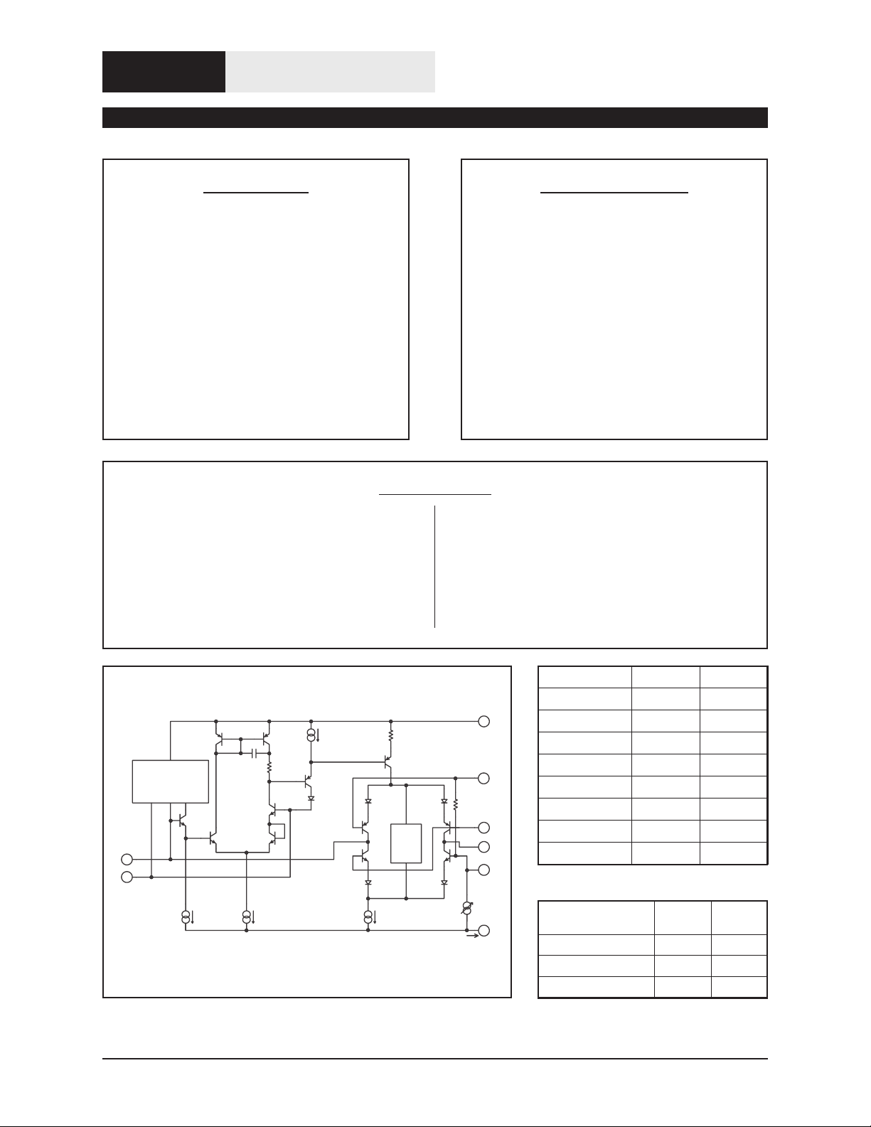
BIAS CURRENT
COMPENSATION
Input
1
6
Gnd
Pin Name SIP Pin SO Pin
7
Iset
25
Vcc
2
Ec+
Ec-
3
8
Output
4
Sym
5
Table 1. 2181 Series Pin Assignments
V-
Max Trimmed THD
@1V,1kHz,0dB
2k
Vbe
MULTI-
PLIER
Iadj
Figure 1. 2181 Series Equivalent Circuit Diagram
THAT Corporation; 45 Sumner Street; Milford, Massachusetts 01757-1656; USA
Tel: +1 508 478 9200; Fax: +1 508 478 0990; Web: www.thatcorp.com
Input 1 1
Ec+ 2 2
Ec– 3 3
Sym 4 4
V– 5 5
Gnd 6 6
V+ 7 7
Output 8 8
Plastic
SIP
Plastic
SO
0.005% 2181LA 2181SA
0.008% 2181LB 2181SB
0.02% 2181LC 2181SC
Table 2. Ordering Information
Page 2 THAT2181 Series IC VCAs
SPECIFICATIONS
1
Absolute-Maximum Ratings (TA=25° C)
Positive Supply Voltage (VCC) +20 V
Negative Supply Voltage (V
Supply Current (I
Max DEE
)10mA
CC
-(EC-) ±1V
C+
) -20 V
EE
Power Dissipation (P
)(TA=75°C) 330 mW
D
Operating Temperature Range (T
Storage Temperature Range (T
) 0 to +70°C
OP
) -40 to +125°C
ST
Recommended Operating Conditions
2181A 2181B 2181C
Parameter Symbol Conditions Min Typ Max Min Typ Max Min Typ Max Units
Positive Supply Voltage V
Negative Supply Voltage V
Bias Current I
Signal Current I
IN+IOUT
SET
CC
EE
VCC-VEE= 30 V 1 2.4 3.5 1 2.4 3.5 1 2.4 3.5 mA
I
= 2.4mA — 0.35 2.5 — 0.35 2.5 — 0.35 2.5 mA
SET
+4 +15 +18 +4 +15 +18 +4 +15 +18 V
-4 -15 -18 -4 -15 -18 -4 -15 -18 V
Electrical Characteristics²
2181A 2181B 2181C
Parameter Symbol Conditions Min Typ Max Min Typ Max Min Typ Max Units
Supply Current I
Equiv. Input Bias Current I
Input Offset Voltage V
Output Offset Voltage V
CC
B
OFF(IN)
OFF(OUT)
No Signal — 2.4 4 — 2.4 4 — 2.4 4 mA
No Signal — 2 10 — 2 12 — 2 15 nA
No Signal — ±5— —±5— —±5— mV
R
=20kW
out
0 dB gain — 0.5 1 — 1 2 — 1.5 3 mV
+15 dB gain — 1 3 — 1.5 4 — 3 10 mV
+30 dB gain — 3 12 — 5 15 — 9 30 mV
Gain Cell Idling Current I
IDLE
Gain-Control Constant T
=25°C(T
A
CHIP
@35°C)
—20— —20— —20— mA
-60 dB < gain < +40 dB
E
/Gain (dB) Pin 2 (Fig. 15) 6.0 6.1 6.2 6.0 6.1 6.2 6.0 6.1 6.2 mV/dB
C+
EC-/Gain (dB) Pin 3 -6.2 -6.1 -6.0 -6.2 -6.1 -6.0 -6.2 -6.1 -6.0 mV/dB
Gain-Control TempCo DEC/ DT
CHIP
Ref T
=27°C — +0.33 — — +0.33 — — +0.33 — %/°C
CHIP
Gain-Control Linearity -60 to +40 dB gain — 0.5 2 — 0.5 2 — 0.5 2 %
1 kHz Off Isolation EC+= -360 mV, EC-= +360 mV 110 115 — 110 11 5 110 11 5 — dB
Output Noise e
n(OUT)
20Hz~20kHz
R
= 20kW
out
0 dB gain — -98 -97 — -98 -96 — -98 -95 dBV
+15 dB gain — -88 -86 — -88 -85 — -88 -84 dBV
Voltage at V- V
V-
No Signal -3.1 -2.85 -2.6 -3.1 -2.85 -2.6 -3.2 -2.85 -2.6 V
1. All specifications subject to change without notice.
2. Unless otherwise noted, T
=25°C, VC= +15V, VEE= –15V. Test circuit is as shown in Figure 2. SYM ADJ is ad
A
justed for minimum THD at 1 V, 1 kHz, Ec– = –Ec+=0V
THAT Corporation; 45 Sumner Street; Milford, Massachusetts 01757-1656; USA
Tel: +1 508 478 9200; Fax: +1 508 478 0990; Web: www.thatcorp.com
-
600030 Rev 01 Page 3
Electrical Characteristics (Cont'd.)
2181A 2181B 2181C
Parameter Symbol Conditions Min Typ Max Min Typ Max Min Typ Max Units
Total Harmonic Distortion THD 1 kHz
= 0 dBV, 0 dB gain — 0.0025 0.005 — 0.004 0.008 — 0.005 0.02 %
V
IN
V
= +10 dBV, -15 dB gain — 0.018 0.025 — 0.025 0.035 — 0.035 0.07 %
IN
V
= -5 dBV, +15 dB gain — 0.018 0.025 — 0.025 0.035 — 0.035 0.07 %
IN
VIN= +10 dBV, 0 dB gain — 0.004 0.008 — 0.006 0.010 — .0015 — %
Slew Rate Rin=R
Symmetry Control Voltage V
Gain at 0 V Control Voltage E
SYMAV
= 0 dB, Minimum THD -0.5 — +0.5 -1.5 — +1.5 -2.5 — +2.5 mV
C-
2181
Series
VCA
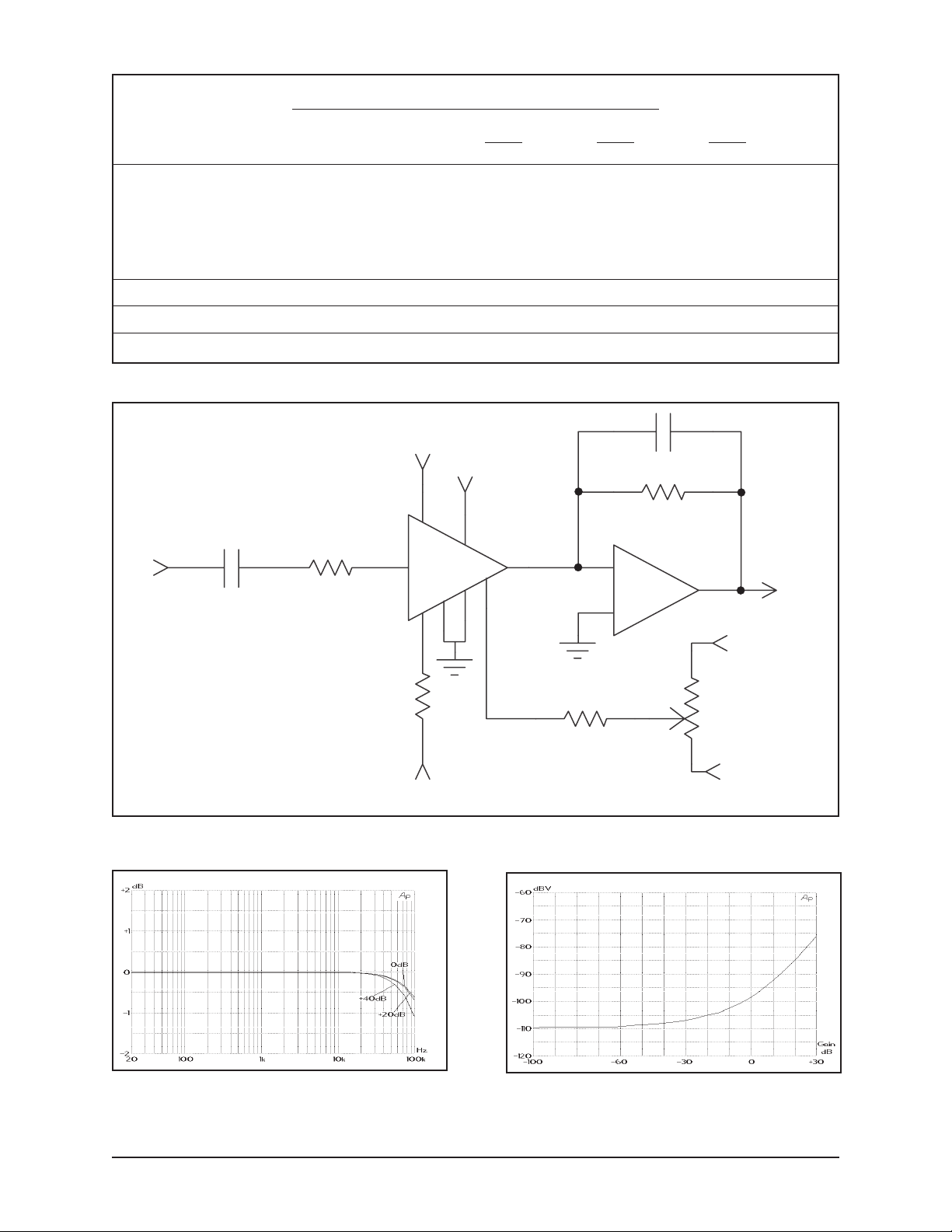
IN
10u
Power Supplies
Vcc = +15 V
Vee=-15V
20k
=20kW —12 — —12 — —12 —V/ms
out
= 0 mV -0.1 0.0 +0.1 -0.15 0.0 +0.15 -0.2 0.0 +0.2 dB
Vcc
Ec-
7
3
V+
-IN
V-
GND
5
Ec-
Ec+
6
1
SYM
2
OUT
8
4
22p
-
OP275
+
20k
OUT
Vcc
5.1k
Rsym
50k
SYM
ADJ
680k (2181A)
220k (2181B)
130k (2181C)
Vee
Vee
Figure 2. Typical Application Circuit
Figure 3. 2181 Series Frequency Response Vs. Gain
THAT Corporation; 45 Sumner Street; Milford, Massachusetts 01757-1656; USA
Tel: +1 508 478 9200; Fax: +1 508 478 0990; Web: www.thatcorp.com
Figure 4. 2181 Series Noise (20kHz NBW) Vs. Gain
 Loading...