

THAT Corporation THAT2155, THAT2151, THAT2150A Datasheet
THAT Corporation
IC Voltage-Controlled
Amplifiers
THAT 2151, 2150A, 2155
FEATURES
• Wide Dynamic Range: >116 dB
• Wide Gain Range: >130 dB
• Expo nential (dB) Gai n Control
• Low Distortion: (0.008% @ 0 dB
gain, 0.035% @15dB gain)
• Wide Gain-Bandwidth: 6 MHz
• Low Cost: $2.20 in ’000s (2155)
• Single In-L ine Packa ge
• Dual Gain-Control Ports (pos/neg)
Description
The THAT 2150 Series integra te d -c ircuit volt age controlled amplifiers (VCAs) are high-performance
current-in/current-out devices with two opposingpolarity, voltage-sensitive control ports. Based on
dbx technology, they offer wide-range exponential
control of gain and attenuation with low signal distortion . The pa rts are h oused in a sp ace-efficient,
plastic 8-pin single-in-line (SIP) package, and re-
APPLICATIONS
• Faders
• Panners
• Compressors
• Expanders
• Equalizers
• Filters
• Oscillators
• Automation Systems
quire minimal support circuitry. Fabricated in a
super low-nois e process utilizing high hFE, complementary NPN/PNP pairs, the 2150 Series VCAs
combine high gain-bandwidth product with low
noise, low distortio n, and l ow offse t to offer d i s cr e te
performance at IC prices. They are available in
three grades, selected for distortion, allowing the
user to optimize cost vs. performance.
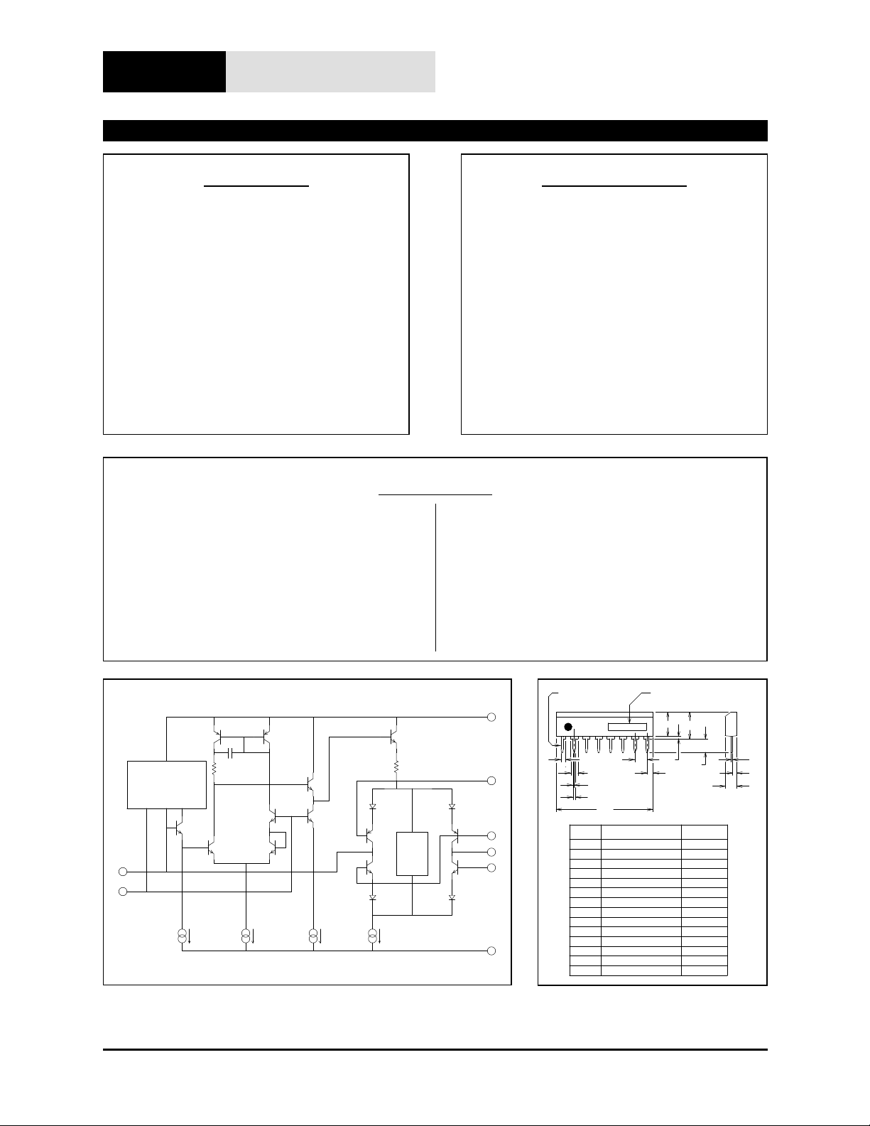
BIAS CURRENT
COMPENSATION
1
6
Vbe
MULTI-
PLIER
Figure 1. 215 0 S e rie s Equi v a le n t Circuit Diagr am
dbx is a registered trademark of Ca r illon Electronics Co r p ora tion
THAT Corporation; 734 Fo rest Street; Marlborou g h , Mas sach usetts 01752; USA
Tel: (508) 229-2500; Fax: (508) 229-2590; Web: http://www.thatcorp.com
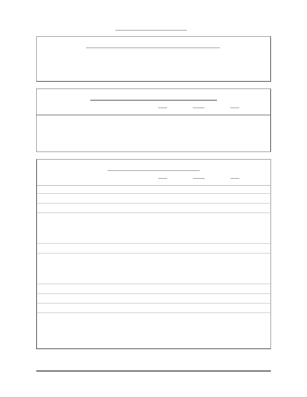
PIN 1
7
2
THAT
N
TYP.
B
D
C
MODEL NO.
H
J
GE
M
F
L
K
I
A
3
8
4
5
ITEM MILLIMETERS INCHES
A 20.32 MAX.
B
1.1 MIN.
+_
.1
C
0.5
0.25
D
2.54
E
F
1.27 MAX.
G
0.51 MIN.
H
5.08 MAX.
+
_
.2
2.8
I
5.75 MAX.
J
1.5 MAX.
K
L
MN3.2
0.25
1.1 MIN.
_
+.10
.04
+
_
.5
0.8 MAX.
0.043 MIN.
_
+
0.02
0.01
0.1
0.05 MAX.
0.02 MIN.
0.2 MAX.
+
_
.008
0.11
0.227 MAX.
0.058 MAX.
.004 .002+
0.01
0.126
0.043 MIN.
.004
+
_
_
.02
Figure 2. 2150 Series Physical Outline
Page 2 2150 Series IC VCAs
SPECI FICATIONS
1
Absolute-Maximum Ratings (TA = 25˚C)
Positive Supply Voltage (VCC) +18 V
Negative Supply Voltage (VEE) -18 V
Supply Current (ICC)10 mA
Power Dissipation (PD) (TA = 75˚C) 330 mW
Operating Temperature Range (TOP) -20 to +75˚C
Storage Tempe rat ur e R an g e ( TST) -40 to +125˚C
Recommended Operating Conditions
2151 2150A 2155
Parameter Symbol Conditions Min Typ Max Min Typ Max Min Typ Max Units
Positive Supply Voltage V
Negative Supply Voltage V
Bias Current I
Signal Current I
IN+IOUT
SET
CC
EE
VCC-VEE= 24 V — 2.4 4 — 2.4 4 — 2.4 4 mA
I
= 2.4 mA — 175 750 — 175 750 — 125 550 µArms
SET
Electrical Characteristics
+5 +12 +15 +5 +12 +15 +5 +12 +15 V
-5 -12 -15 -5 -12 -15 -5 -12 -15 V
2
2151 2150A 2155
Parameter Symbol Conditions Min Typ Max Min Typ Max Min Typ Max Units
Supply Current I
Equiv. Input Bias Current I
Input Offset Voltage V
Output Offset Voltage V
Gain Cell Idling Current I
Gain-Control Constant T
Gain-co nt rol Temp Co ∆ EC / ∆ T
Gain-Control Linearity -60 to +40 dB gain — 0.5 2 — 0.5 2 — 0.5 2 %
Off Isolation (Fig. 14) EC+=-360mV, EC-=+360mV 110 115 — 110 115 110 115 — dB
Output Noise e
CC
B
OFF(IN)
OFF(OUT)
IDLE
/Gain (dB) Pins 2 & 4 (Fig. 14) 6.0 6.1 6.2 6.0 6.1 6.2 6.0 6.1 6.2 mV/dB
E
C+
EC-/Gain (dB) Pin 3 -6.0 -6.1 -6.2 -6.0 -6.1 -6.2 -6.0 -6.1 -6.2 mV/dB
CHIP
n(OUT)
No Signal — 2.4 4 — 2.4 4 — 2.4 4 mA
No Signal — 5 8 — 5 8 — 5 8 nA
No Signal — +10 — — +10 — — +10 — mV
R
=20 kΩ
out
0 dB gain — 1 3 — 1 3 — 1 3 mV
+15 dB gain — 2 3 — 2 3 — 2 3 mV
+40 dB gain — 5 15 — 7 15 — 10 15 mV
—20— —20— —20— µA
=25˚C (T
A
-60 dB < gain < +40 dB
Ref T
20 Hz-20 kHz
R
+15 dB gain — -88 -86 — -88 -86 — -88 -86 dBV
≅35˚C)
CHIP
= 27˚C — +0.33 — — +0.33 — — +0.33 — %/˚C
CHIP
= 20kΩ
out
0 dB gain — -98 -97 — -98 -96 — -98 -96 dBV
1. All specifications subject to change without notice.
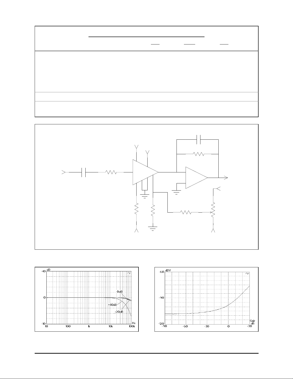
2. Unless otherwise noted, TA=25˚C, VCC = +15V, VEE= -15V. Test circuit is as shown in Figure 3. SYM
justed for minimum THD @ Vin=1 V, 1 kHz, 0 dB gain.
THAT Corporation; 734 Fo rest Street; Marlborou g h , Mas sach usetts 01752; USA
Tel: (508) 229-2500; Fax: (508) 229-2590; Web: http://www.thatcorp.com
ADJ
is ad-
Rev. 10/25/96 Page 3
Electrical Characteristics (Cont’d.)
2151 2150A 2155
Parameter Symbol Conditions Min Typ Max Min Typ Max Min Typ Max Units
Total Harmonic Distortion THD IIN+ I
= 180 µA, 1 kHz
OUT
0 dB gain — 0.004 0.02 — 0.005 0.03 — — — %
±15 dB gain — 0.025 0.045 — 0.05 0.07 — — — %
+ I
= 150 µA, 1 kHz
I
IN
OUT
0 dB gain — — — — — — — 0.006 0.03 %
±15 dB gain — — — — — — — 0.05 0.07 %
Symmetry Control Voltage V
Gain at 0 V Control Voltage E
AV= 0 dB, THD < 0.07% -1.6 0 +1.6 -2 0 +2 -2.5 0 +2.5 mV
SYM
INPUT
10u
= 0 mV -0.1 0.0 +0.1 -0.15 0.0 +0.15 -0.2 0.0 +0.2 dB
C–
+15V
-
LF351
+
47p
20k
OUTPUT
20k
Ec-
2150
GND
Series
VCA
3
Ec-
OUT
Ec+
Ec+
6
8
4
2
7
V+
1
-IN
V-
5
+15V
5.1k
51
Rsym
150k
300k (2155)
390k (2150A)
470k (2151)
50k
SYM
ADJ
Figure 3. Typical Application Circuit
Figure 4. Frequency Response Vs. Gain (2150A)
THAT Corporation; 734 Fo rest Street; Marlborou g h , Mas sach usetts 01752; USA
Tel: (508) 229-2500; Fax: (508) 229-2590; Web: http://www.thatcorp.com
-15V-15V
Figure 5. Noise (20kHz NBW) Vs. Gain (2150A)
 Loading...