

THAT CORPORATION THAT1570, THAT5171 User Manual

THAT1570/THAT5171
A
Digitally-Controlled Microphone Preamplifier
Demo Board
User's Guide
Document 600134 Rev 02
Contents
Features/Specifications....................................................................................... 3
Overview ............................................................................................................ 4
Connections ....................................................................................................... 5
Hardware Set-up ................................................................................................. 5
Software Set-up ................................................................................................... 6
Operation ........................................................................................................... 7
Jumper Options ................................................................................................. 7
Appendix A - Schematic...................................................................................... 9
Appendix B - Bill of Materials............................................................................. 10
Appendix C - PCB Layout .................................................................................. 12
THAT Corporation; 45 Sumner Street; Milford, MA 01757-1656; US
Tel: +1 508 478 9200; Fax: +1 508 478 0990; Web: www.thatcorp.com
Copyright © 2009, THAT Corporation; All rights reserved.

Document 600134 Rev 02 Page 2 of 16 THAT 1570/5171-DEMO User’s Guide
A
Packing List
(1) THAT1570/5171 DEMO Board PCB Assembly
(1) USB Cable
(1) Software CD
If you are missing any of the above items please contact us at
support@thatcorp.com.
FCC Warning
This device is only intended for laboratory test environments. It may radiate radio
frequency energy and has not been tested for compliance with subpart J of part
15 of the FCC regulations. Operation of this device in other environments may
cause interference with radio communications.
THAT Corporation; 45 Sumner Street; Milford, MA 01757-1656; US
Tel: +1 508 478 9200; Fax: +1 508 478 0990; Web: www.thatcorp.com
Copyright © 2009, THAT Corporation; All rights reserved.
Document 600134 Rev 02 Page 3 of 16 THAT 1570/5171-DEMO User’s Guide
A
Features
• “Combo” XLR/TRS balanced input with switchable 48V phantom power
• Balanced audio output on XLR and TRS connectors
• Supports pro audio signal levels: +21dBu input / output
• Gain (measured input to output) adjustable in 1dB steps: 0dB, and 8-63dB
• USB 1.1 and USB 2.0 compatible control port
• Graphical user interface software for controlling 5171 parameters
• Prototyping area
Description
The THAT Digitally-Controlled Mic Preamp Demo Board allows developers to
evaluate the performance of the THAT1570 / THAT5171 chipset. The demo
board provides a balanced audio input on a Neutrik “combo” connector with 48V
phantom power, and a balanced audio output on XLR and ¼” TRS connectors.
The supplied graphical user interface (GUI) controls all functions in the 5171 chip
via USB. A prototyping area is available for adding or modifying circuitry.
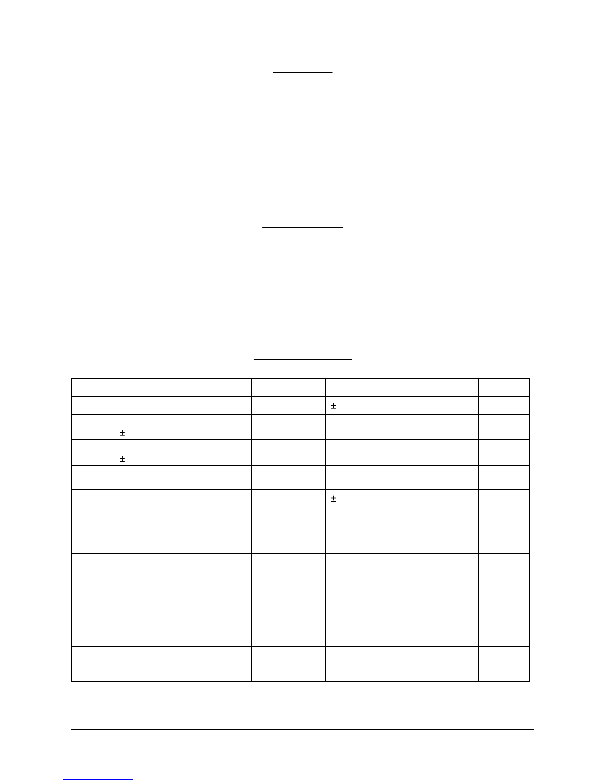
Maximum Input Level
(V+ /V- = ±15V)
Maximum Differential Output Level
(V+ /V- = ±15V)
Gain (input to output)
Gain error (all settings)
Total Harmonic Distortion
(V
= +16dBu (5V
OUT
= 10 pF; f = 1kHz; BW = 22 kHz)
C
L
); RL = 10kΩ;
RMS
Equivalent Input Noise
(main output)
Equivalent Input Noise
(1570 output)
Supply Current
Specifications
V+ - V-Power Supply Voltage
in-BAL
OUT
A
dB
A
err
THD
EIN
EIN
ICC; -IEE, I
DD
±
15
0
8 to 63 in 1dB steps
±
0.15
0.0003 (0dB gain)
0.0003 (20dB gain)
0.0008 (40dB gain)
0.006 (60dB gain)
1.65 (60dB gain)
1.9 (40dB gain)
5.0 (20dB gain)
22.9 (0dB gain)
1.65 (60dB gain)
1.9 (40dB gain)
4.8 (20dB gain)
20 (0dB gain)
23 (V+ supply)
23 (V- supply)
0.5 (+5V supply)
UnitsTypicalSymbolParameter
V
dBu+21v
dBu+21V
dB
dB
%
nV/√Hz
nV/√Hz
mA
THAT Corporation; 45 Sumner Street; Milford, MA 01757-1656; US
Tel: +1 508 478 9200; Fax: +1 508 478 0990; Web: www.thatcorp.com
Copyright © 2009, THAT Corporation; All rights reserved.
Document 600134 Rev 02 Page 4 of 16 THAT 1570/5171-DEMO User’s Guide
A
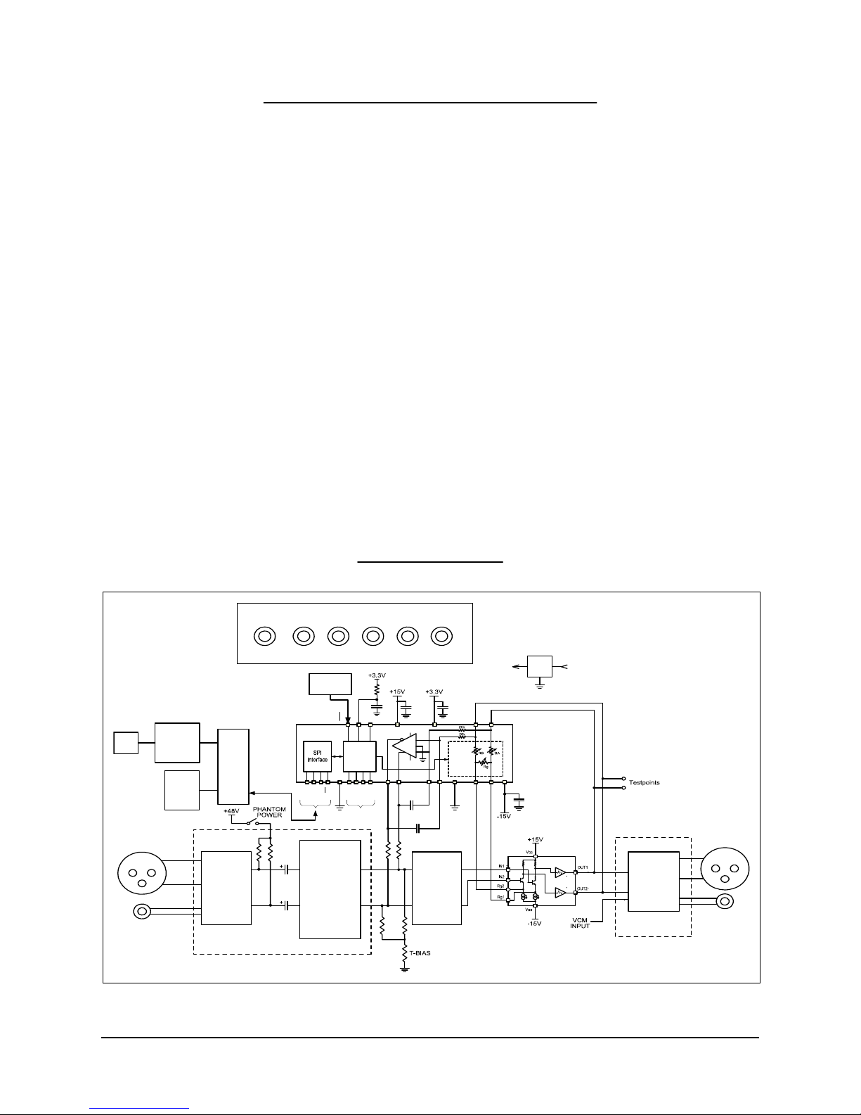
THAT1570 / THAT5171 Overview
The THAT1570 and THAT5171 ICs enable digitally-controlled microphone
preamplifier applications with exceptionally high performance. Operating on
maximum +/-17V supplies, the chipset accepts pro audio input levels (+22dBu
max) without an input pad. Gain is adjustable to 5.6dB, and 13.6dB to 68.6dB in
1dB increments (a 5.6dB attenuator at the output offsets the overall gain range to
0dB, and 8-63dB). The 5171’s built-in zero-crossing detector and other patentpending techniques for reducing zipper noise enable very smooth and silent gain
changes. A differential servo reduces output offsets to less than 1.5mV. Four
general purpose outputs on the 5171 can be connected to a variety of peripheral
functions, e.g. an input pad, phantom power switch, signal routing switches,
LEDs, etc. The 5171’s addressable SPI interface supports read-back. By separating the analog mic pre amp front end (THAT1570) from the digital functions and
switched resistor ladder (THAT5171), each IC is optimized for high performance.
The THAT1570 is fabricated using THAT’s complementary dielectric isolation
process and precision laser-trimmed Si-Chrome thin film resistors, yielding
extremely high performance. The THAT5171 is fabricated using a high-voltage
CMOS process, with proprietary techniques for reducing FET switching glitches.
Packaged in 4x4mm QFN16 and 7x7mm QFN32 packages respectively, the
THAT1570 and THAT5171 require very little PCB area.
USB
Mic/Line
Input
USB
Interface
Ext
SPI
Conn
MUX
RFI
Protection
+48VCHAS +15 V -15 V +5VGND
U1
THAT
5171
SPI Bus
INPUT SECTION
Power Supply Inputs
Reset
Switch
CS
DIN
SCLK
DOUT
Phantom
Power
Fault
Protection
Block Diagram
RST
BSY
TRC
Control
Logic
DGnd
GPO1
GPO2
GPO3
GPO0
SOUT2
LEDs
Vdd
Vcc
Vcc
+
-
Servo
+
-
SCAP2
SCAP1
RFI
Protection
with FET
Switches
Vee
SOUT1
Resistor
Network
AGnd
IN2
Rg2
+3.3V +5V
REG
IN1
Vee
Rg1
U2
THAT
1570
Balanced
Output
Driver
OUTPUT
SECTION
Balanced
Output
Figure 1 -- Block Diagram of the THAT 1570/5171 Demo Board
THAT Corporation; 45 Sumner Street; Milford, MA 01757-1656; US
Tel: +1 508 478 9200; Fax: +1 508 478 0990; Web: www.thatcorp.com
Copyright © 2009, THAT Corporation; All rights reserved.

Document 600134 Rev 02 Page 5 of 16 THAT 1570/5171-DEMO User’s Guide
A
Connections
Power
The USB interface runs on USB bus power, but the rest of the demo board
requires an external power supply. +/-15 V (maximum +/-17V) supplies the
analog circuitry. +48V phantom power is input (not generated on the board) and
switched on and off via the on-board Phantom Power switch. Note that the ground
return for +48V phantom power is via the CHAS (chassis ground) connector. The
+5V input is regulated on board to 3.3V and supplies the digital logic.
Audio Input
The Neutrik combo connector accepts an XLR or ¼” TRS cable. Maximum input
signal level is +21dBu with +/-15V supplies, or +22dBu with +/-17V supplies.
The 1/4” TRS signal path includes a 20dB pad in order to support very high line
levels.
Audio Output
Separate XLR and ¼” TRS connectors are wired in parallel. Maximum output
signal level is +21dBu with +/-15V supplies, or +22dBu with +/-17V supplies.
The differential attenuator/output buffer (U3) adds a small amount of noise and
distortion to the signal and it is therefore recommended that test points TP1-TP3
be used to measure performance of the 1570/5171 ICs.
USB
A PC must be plugged into the demo board via USB in order to control parameters in the 5171 (e.g. gain). Take care not to hot plug the demo board while the
GUI software is running as this will often crash the Windows drivers.
General Purpose Outputs (GPO)
The GPO3:0 pins are connected to header J12. J12 is conveniently located near
the prototyping area, so the user can easily connect optional circuitry to them.
Note that the GPO pins are also connected to LEDs, D1-D4, and pull up and pull
down resistors which set the 5171 device address during reset. Consideration
must be given to how any application circuitry that is added interacts with these
other functions.
Hardware Set-up
1. Connect a power supply to the V+, V-, +5V, +48V, CHAS and GND
connectors. Do not turn on power yet.
2. Plug in the audio input and output
3. Attach a USB cable to the demo board, but do not plug it into the PC yet
4. Turn on the power supply
5. Turn on phantom power to microphone (if appropriate)
6. Plug USB cable into PC. Windows should go through its procedure for discovering the new USB peripheral and loading its driver.
THAT Corporation; 45 Sumner Street; Milford, MA 01757-1656; US
Tel: +1 508 478 9200; Fax: +1 508 478 0990; Web: www.thatcorp.com
Copyright © 2009, THAT Corporation; All rights reserved.
 Loading...