

THAT Corporation THAT1440, THAT1430, THAT1420 Datasheet
THAT Corporation; 45 Sumner Street; Milford, Massachusetts 01757-1656; USA
Tel: +1 (508) 478-9200; Fax: +1 (508) 478-0990; Web: www.thatcorp.com
THAT 1420, 1430
Description
The THAT 1420 and 1430 are a new genera
tion of audio differential line drivers with improved performance over conventional
cross-coupled monolithic designs. Both models
exhibit low noise and distortion, high slew rate,
stability under difficult loads, wide output swing,
and have outputs which are short-circuit protected.
In addition both models incorporate patented
OutSmartsÔ technology, a dual feedback-loop de
sign that prevents the excessive ground currents
typical of cross-coupled output stages (CCOS)
when clipping into single-ended loads
1
.
To overcome this problem, the THAT 1420
and 1430 use two individual negative-feedback
loops to separately control the differential output
voltage and common mode output currents, mak
-
ing the design inherently more stable and less
sensitive to component tolerances than the CCOS.
Most importantly, the dual-feedback design prevents the loss of common-mode feedback that
plagues the CCOS designs, avoiding the excessive
ground currents and overly-distorted output
waveform that can result when driving single-ended loads.
Where minimum output offset voltage with
minimum parts count is desired, the THAT 1430
further improves over existing designs. In con
ventional CCOS circuits, two relatively high-value
electrolytic capacitors are required to reduce the
offset voltage. By contrast, the THAT 1430 topol
ogy requires only a resistor and a single film or
ceramic capacitor to achieve the same effect at
lower parts count and price.
THAT Corporation
OutSmartsä Balanced Line Drivers
FEATURES
·
OutSmartsÔ technology tames
clipping behavior into single-ended
loads
·
Pin-compatible with SSM2142
·
Balanced, floating output delivers
transformer-like behavior
·
Stable when driving long cables
and capacitive loads
·
THAT 1430 delivers low output
offset voltage using single capacitor
APPLICATIONS
·
Differential Line Driver
·
Audio Mix Consoles
·
Distribution Amplifiers
·
Audio Equalizers
·
Dynamic Range Processors
·
Digital Effects Processors
·
Telecommunications Systems
·
Instrumentation
·
Hi-Fi Equipment
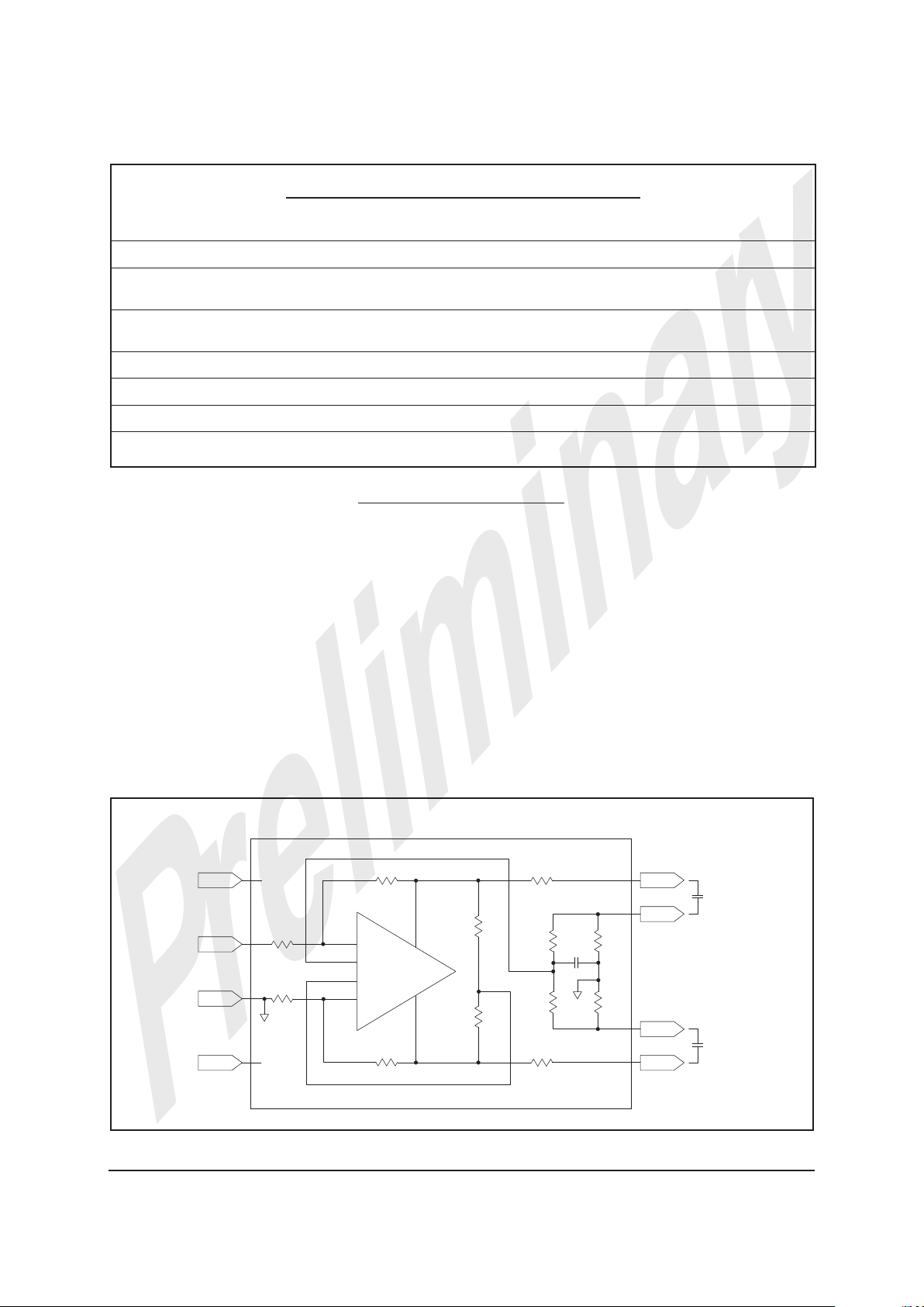
Din+
Cin+
Cin-
Din-
Out-
Sens+
Out+
Sens-
Vcc
In+
Vee
Gnd
Dout-
Dout+
10k
10k
50
5k
5k
10k
10k
10k
10k
20k
20k
10p
50
THAT 1420
CEXT
CEXT
D
C
AA
&
Figure 1. THAT 1420 Equivalent Circuit Diagram
1. See Gary Hebert’s paper, An Improved Balanced, Floating Output Driver IC, presented at the 108th AES Convention, Feb. 2000
DIP Pin
Number
SO Pin
Number
1420 Pin
Name
1430 Pin
Name
1 3 Out- Out-
2 4 Sens- Cap2
35GndGnd
4 6 In In
5 11 Vee Vee
6 12 Vcc Vcc
7 13 Sens+ Cap1
8 14 Out+ Out+
Table 1. THAT 1420/1430 pin assignments
THAT Corporation; 45 Sumner Street; Milford, Massachusetts 01757-1656; USA
Tel: +1 (508) 478-9200; Fax: +1 (508) 478-0990; Web: www.thatcorp.com
Page 2 THAT1420/1430 Balanced Line Driver
Preliminary Information
Absolute Maximum Ratings (TA= 25°C)
Positive Supply Voltage (Vcc) +18 V Operating Temperature Range (TOP) -40 to +85°C
Negative Supply Voltage (Vee) -18 V Storage Temperature (T
ST
) -40 to +150°C
Output Short Circuit Duration Continuous Junction Temperature (T
J
) 150°C
Power Dissipation (P
D
) TBD mW Lead Temperature (T
LEAD
)(Soldering 60 sec) 300°C
SPECIFICATIONS
2
2. All specifications are subject to change without notice.
3. All measurements taken with V
S
=±18, T=25°C, unless otherwise noted
Electrical Characteristics
3
Parameter Symbol Conditions Min. Typ. Max. Units
Input Impedance Z
IN
45 kW
Gain G1 R
L
=600W
Balanced 4.35 4.65 4.95 dB
Single Ended 4.4 4.6 4.8 dB
Gain G2 R
L
=100kW
Balanced 5.8 6 6.2 dB
Single Ended 5.8 6 6.2 dB
DC Power Supply
Rejection Ratio PSRR ±4V to ±18V 80 105 dB
Output Common-Mode
Rejection Ratio OCMRR f=1kHz, BBC Method 50 68 dB
Output Signal Balance Ratio SBR f=1kHz, BBC Method 28 40 dB
THD+N (Balanced) THD+N
1
20Hz-20kHz 0.001 %
1kHz 0.0005 %
THD+N (Single Ended) THD+N
2
VO=10 V
RMS,RL
=600W, 20Hz-20kHz 0.0018 %
Output Noise SNR Bal. Mode, 20 kHz BW -104 dBV
Headroom HR 0.1% THD+N 25 dBV
Slew Rate SR 16 V/mS
Output Common Mode
Voltage Offset V
OCM
RL=600W, w/o Sense capacitors -300 ±60 300 mV
THAT1420 V
OCM
RL=600W, w/ Sense capacitors -6 ±4 6 mV
Output Common Mode
Voltage Offset V
OCM
RL=600W, w/o Sense capacitor -400 ±80 400 mV
THAT1430 V
OCM
RL=600W, w/ Sense capacitor -20 ±10 20 mV
Theory of Operation
OutSmartsÔ technology
The THAT 1420 and 1430 are similar devices,
both employing the OutSmarts topology, a variation
of circuitry originally developed at Audio Toys, Inc.
OutSmarts topology employs two negative-feedback
loops -- one to control the differential signal, and a
separate loop to control the common mode output
levels.
Figures 2 and 3 show the gain core common to
both the THAT 1420 and 1430. The gain core is a
single amplifier that includes two differential input
pairs, C
in+/-
and D
in+/-
, and complementary outputs,
V
out+
and V
out-,
related to each other by two gain ex
-
pressions, A
D
(s) and AC(s). The first pair of differen
-
tial inputs, D
in+/-
, are connected to the differential
feedback network between the outputs and the input
signal. The second differential input pair, C
in+/-
,is
connected to a bridge circuit which generates an error signal that is used to servo the common-mode behavior of the outputs. The loop equations are then,
()
DD DADD
OUT OUT OUT D IN IN+- +-
-= = -D
where A
D
is the differential open-loop gain, and
()
DD DACC
OUT OUT OUT C IN IN+- +-
+= = -
å
where ACis the common-mode open-loop gain.
THAT Corporation; 45 Sumner Street; Milford, Massachusetts 01757-1656; USA
Tel: +1 (508) 478-9200; Fax: +1 (508) 478-0990; Web: www.thatcorp.com
Rev. 4/24/01 Page 3
Preliminary Information
Electrical Characteristics (cont’d.)
Parameter Symbol Conditions Min. Typ. Max. Units
Differential Output Offset V
OOD
RL=600W -10 ±4 10 mV
Differential Output
Voltage Swing,Pos V
IN
= ±18V VCC-2 V
Differential Output
Voltage Swing,Neg V
IN
= ±18V VEE+2 V
Output Impedance Z
O
40 50 60 W
Quiescent Supply Current I
S
Unloaded, VIN= 0 4 5.2 mA
Short Circuit Output Current I
SC
60 70 mA
Voltage Supply Range ±4 ±18 V
Din+
Cin+
Cin-
Din-
Out-
Sens+
Out+
Sens-
Vcc
In+
Vee
Gnd
Dout-
Dout+
10k
10k
50
5k
5k
10k
10k
10k
10k
20k
20k
10p
50
THAT 1420
CEXT
CEXT
D
C
AA
&
Figure 2. THAT 1420 Equivalent Circuit Diagram
 Loading...