

THAT Corporation THAT1246, THAT1240, THAT1243 Datasheet
THAT Corporation
Balanced Line Receiver ICs
THAT 1240, 1243, 1246
FEATURES
High CMRR: typically 90dB at 60Hz
·
Wide bandwidth and high slew rate
·
Low distortion and low noise
·
Available in 0 dB, -3 dB, and -6 dB
·
versions
Pin compatible with SSM2143 and
·
INA137
Description
The THAT 124x series of precision differential
amplifiers are designed primarily for use as audio
balanced line receivers. Gains of 0 db, -3 dB, and
-6 dB are available to suit various applications requirements.
The THAT 1246 is drop-in compatible with
the Burr-Brown INA137 and Analog Devices
SSM2143, while the THAT 1240 is drop-in compatible with the SSM2140.
All devices exhibit 90 dB of typical common-mode rejection, slew rates of 12 V/ms, a
APPLICATIONS
Balanced Audio Line Receivers
·
Summing Amplifiers
·
Differential Amplifiers
·
Current Shunt Monitors
·
Ground Loop Eliminator
·
20MHz bandwidth, and 0.0006% THD. Both sur
face-mount and DIP packages are available.
The THAT 124x family are laser-trimmed to
obtain the precision resistor matching needed for
high CMR performance. Fashioned in THAT Corporation's proprietary dielectric isolation (DI)
process, the THAT 124x series provides the sonic
benefit of discrete designs, with the compact size,
reliability, matching, and thermal tracking of a
fully integrated solution.
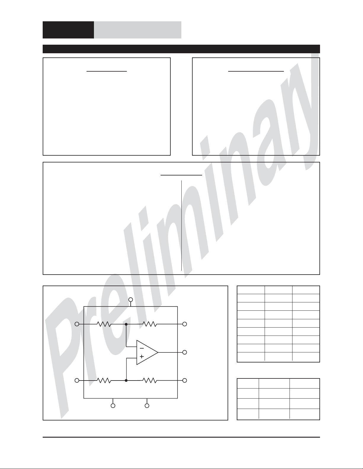
-
Vcc
In-
In+
Vee
Figure 1. THAT1240-series equivalent circuit diagram
THAT Corporation; 45 Sumner Street; Milford, Massachusetts 01757-1656; USA
Tel: +1 (508) 478-9200; Fax: +1 (508) 478-0990; Web: www.thatcorp.com
NC
Sense
Vout
Ref
Pin Name DIP Pin SO Pin
Ref 1 1
In- 2 2
In+ 3 3
Vee 4 4
Sense 5 5
Vout 6 6
Vcc 7 7
NC 8 8
Table 1. 1240 Series pin assignments
Gain Plastic DIP Plastic SO
0 dB 1240P 1240S
-3 dB 1243P 1243S
-6 dB 1246P 1246S
Table 2. Ordering information
Page 2 Balanced Line Receiver ICs
Preliminary Information
SPECIFICATIONS
1
Absolute Maximum Ratings (TA= 25°C)
Positive Supply Voltage (VCC) +18 V Power Dissipation (PD)(TA= 75°C) TBD mW
Negative Supply Voltage (V
Storage Temperature Range (T
Output Short-Circuit Duration (t
) -18 V Operating Temperature Range (TOP) 0 to +70°C
EE
) -40 to +125°C Junction Temperature (TJ) 150°C
ST
) Continuous Lead Temperature (Soldering 60 seconds) TBD °C
SH
Positive Input Voltage (Ref, Sense) +18 V Negative Input Voltage (Ref, Sense) -18 V
THAT1240 THAT1243 THAT1246
Positive Input Voltage (In+,In-) Vcc x 2 Vcc x 2.4 Vcc x 3
Negative Input Voltage (In+, In-) Vee x 2 Vee x 2.4 Vee x 3
Recommended Operating Conditions
Parameter Symbol Conditions Min Typ Max Units
Positive Supply Voltage V
Negative Supply Voltage V
CC
EE
+2.2 +18 V
-2.2 -18 V
Electrical Characteristics
2
Parameter Symbol Conditions Min Typ Max Units
Supply Current I
Input Voltage Range V
CC
IN-DIFF
Differential (equal and opposite swing)
No signal — 2.1 3.4 mA
THAT1240 (0 dB gain) — 21.5 — dBu
THAT1243 (-3 dB gain) — 24.5 — dBu
THAT1246 (-6 dB gain) — 27.5 — dBu
V
IN-CM
Common mode
THAT1240 (0 dB gain) — 27.5 — dBu
THAT1243 (-3 dB gain) — 29.1 — dBu
THAT1246 (-6 dB gain) — 31.0 — dBu
Input Impedance
4
Z
Z
IN-DIFF
IN-CM
Common mode (all versions) — 9 — kW
Differential
THAT1240 — 18 — kW
THAT1243 — 21 — kW
THAT1246 — 24 — kW
Common Mode Rejection CMR Matched source impedances; VCM= ±10V
DC 70 90 — dB
60 Hz 70 90 — dB
20 kHz — 85 — dB
44 kHz — 60 — dB
Power Supply Rejection
5
PSR At 60 Hz, with VCC=-V
EE
THAT1240 — 82 — dB
THAT1243 — 80 — dB
3
1. All specifications are subject to change without notice.
2. Unless otherwise noted, T
3. 0 dBu = 0.775Vrms.
4. See test circuit in Figure 2.
5. Defined with respect to differential gain.
=25°C, VCC= +15V, VEE= -15V, Gain=-6dB
A
THAT Corporation; 45 Sumner Street; Milford, Massachusetts 01757-1656; USA
Tel: +1 (508) 478-9200; Fax: +1 (508) 478-0990; Web: www.thatcorp.com

Rev. 04/29/02 Page 3
Preliminary Information
Electrical Characteristics (Cont’d)
Parameter Symbol Conditions Min Typ Max Units
Total Harmonic Distortion THD V
=10dBV;BW=20kHz;f=1kHz
IN-DIFF
R
=2kW — 0.0006 — %
L
Output Noise e
n(OUT)
BW=20kHz
THAT1240 — -106 — dBu
THAT1243 — -107 — dBu
THAT1246 — -109 — dBu
Slew Rate SR RL=2kW;CL= 300 pF 7 12 — V/µs
Small Signal Bandwidth BW
-3dB
RL=2kW;CL=10pF
THAT1240 12 24 — MHz
THAT1243 17 33 — MHz
THAT1246 23 44 — MHz
R
=2kW;CL= 300 pF
L
THAT1240 11 17 — MHz
THAT1243 13 18 — MHz
THAT1246 14 20 — MHz
Output Gain Error G
ER(OUT)
Output Voltage Swing V
Output Offset Voltage V
Output Short Circuit Current I
Resistive Load R
Capacitive Load C
O
OFF
SC
Lmin
Lmax
f = 1 kHz — ±0.03 ±0.5 %
RL=2kW ±12.5 ±13 — V
No signal -7 0 +7 mV
RL=0W — ±25 — mA
—— 2 kW
300 — — pF
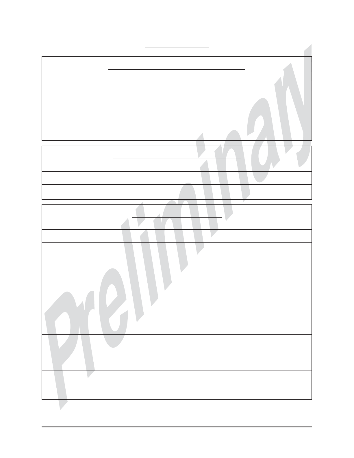
Vcc
In-
½U
diff
~
R
1
b
R
2
Sense
Vout
½U
diff
~
In+
R
3
a
V
~
CM
R
4
Ref
R
L
C
L
Vee
Part no.
THAT1240
THAT1243
THAT1246
Gain
0dB
-3 dB
-6 dB
R=R
13
9k
Ù
Ù
10.5 k
Ù
12 k
R=R
24
9k
Ù
Ù
7.5 k
Ù
6k
Figure 2. THAT1240 series test circuit
THAT Corporation; 45 Sumner Street; Milford, Massachusetts 01757-1656; USA
Tel: +1 (508) 478-9200; Fax: +1 (508) 478-0990; Web: www.thatcorp.com
 Loading...