

THALER VRE4120B, VRE4112C, VRE4112K, VRE4112B, VRE4110K Datasheet
...
VRE4100 Series
Low Cost, SOIC-8
Precision References
THALER CORPORATION • 2015 N. FORBES BOULEVARD • TUCSON, AZ. 85745 • (520) 882-4000
FEATURES
• 1.024, 1.250, 2.048, 2.500, 4.096V Output
• Initial Error: ±0.05% max.
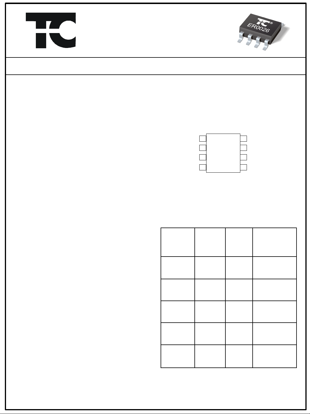
PIN CONFIGURATION
• Temperature Drift: 1.0 ppm/°C max.
• Low Noise: 2.2µV
(0.1Hz-10Hz, 1.024V)
p-p
• Low Thermal Hysterisis: 20ppm
• ±8mA Output Source
• Power Down Mode
• Industry Standard SOIC-8 pin out
• Commercial and Industrial Temp Ranges
• Second source for ADR29X, REF19X ,LT1460,
LT1461, LT1798, MAX616X, REF102
DESCRIPTION
The VRE4100 is a low cost, high precision
bandgap reference that operates from +5V. The
device features low noise, digital error correction,
and an SOIC-8 package. The ultrastable output
is 0.05% accurate with a temperature coefficient
as low as 1.0 ppm/°C. The improvement in
overall accuracy is made possible by using
EEPROM registers and CMOS DAC’s for
temperature and initial error correction. The DAC
trimming is done after assembly which eliminates
assembly related shifts.
The VRE4100 is recommended for use as a
reference for 14, 16, or 18 bit data converters
which require a precision reference. The
VRE4100 offers superior performance over
standard on-chip references commonly found
with data converters.
NC
+V
Enable
GND
1
VRE4100
2
IN
TOP
3
VIEW
4
8
NC
7
NC
6
V
REF
5
NC
FIGURE 1
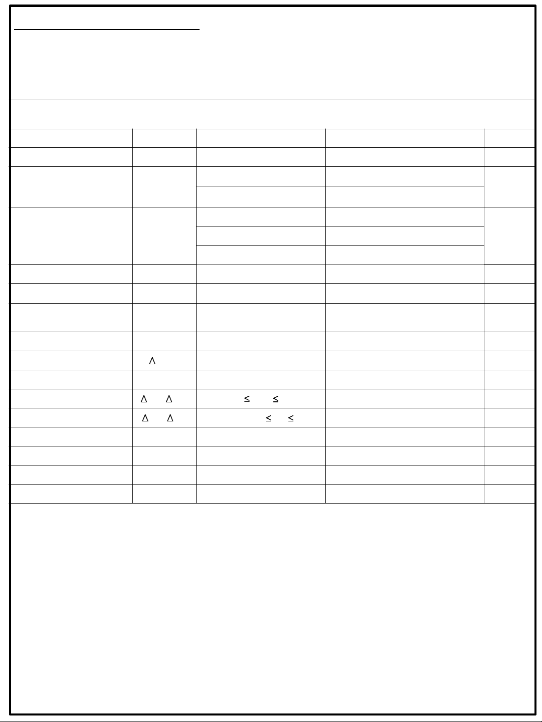
SELECTION GUIDE
Output
Voltage
Model
VRE4110B 1.024 1.0 0°C to +70°C
VRE4110C 1.024 2.0 0°C to +70°C
VRE4110K 1.024 3.0 -40°C to +85°C
VRE4112B 1.250 1.0 0°C to +70°C
VRE4112C 1.250 2.0 0°C to +70°C
VRE4112K 1.250 3.0 -40°C to +85°C
VRE4120B 2.048 1.0 0°C to +70°C
VRE4120C 2.048 2.0 0°C to +70°C
VRE4120K 2.048 3.0 -40°C to +85°C
VRE4125B 2.500 1.0 0°C to +70°C
VRE4125C 2.500 2.0 0°C to +70°C
VRE4125K 2.500 3.0 -40°C to +85°C
VRE4141B 4.096 1.0 0°C to +70°C
VRE4141C 4.096 2.0 0°C to +70°C
VRE4141K 4.096 3.0 -40°C to +85°C
V
Temp.
Coeff.
ppm/°C
Temp.
Range °C
VRE4100DS REV. A MAY 01
ABSOLUTE MAXIMUM RATINGS
Power supply to any input pin ….…-0.3V to +5.6V Output Short Circuit Duration …….…………....Indefinite
Operating Temp. (B,C) …………..……0°C to 70°C ESD Susceptibility Human Body Model…….…..…..2kV
Operating Temp. (K)………………...-40°C to 85°C ESD Susceptibility Machine Model ..………………200V
Storage Temperature Range……..-65°C to 150°C Lead Temperature (soldering,10 sec)………...….260°C
ELECTRICAL SPECIFICATIONS
Vps =+3V for VRE4110 and VRE4112, Vps =+5V for VRE4125, VRE4125 and VRE4141. T = 25°C, I
PARAMETER
=1mA, C
load
=1µF unless otherwise noted.
out
UNITSMIN TYP MAXSYMBOL CONDITIONS
Input Voltage
Output Voltage Error
(Note 1)
Output Voltage
Temperature Coefficient
(Note 2)
Dropout Voltage (Note 3)
Turn-On Settling Time
Output Noise Voltage
(Note 4)
Long Term Stability
Supply Current
Load Regulation (Note 6)
Line Regulation (Note 6)
Logic High Input Voltage
Logic High Input Current
Logic Low Input Voltage
Logic Low Input Current
IN
OUT
OUT
IN -VOUT
ON
n
OUT/T
IN
/ I
OUT
/ V
OUT
H
H
L
L
OUT
V1.8 5.5V
± 0.025% ± 0.050%VRE4100B
± 0.040% ± 0.080%VRE4100C/K
%V
0.5 1.0VRE4100B
1.0 2.0VRE4100C
ppm/°CTCV
1.5 3.0VRE4100K
160 235IL= 8 mA
mVV
µs2 To 0.01% of final valueT
µVp-p2.20.1Hz<f<10HzE
ppm20Note 5Temperature Hysterisis
ppm501000 HoursV
= 0mAI
load
8mAV
Load
IN
+ 200mV V
ref
IN
5.5VV
1 201mA I
µA230 320V
ppm/mA
ppm/V20 200V
V0.8V
nA2I
V0.4V
nA1I
Notes:
1. High temperature and mechanical stress can effect the initial accuracy of the VRE4100 series
references.See discussion on output accuracy.
2. The temperature coefficient is determined by the box method. See discussion on temperature
performance. All units are 100% tested over temperature.
3. The minimum input to output differential voltage at which the output voltage drops by 0.5% from nominal.
4. Based on 1.024V output. Noise is linearly proportional to V
REF.
5. Defined as change in 25°C output voltage after cycling device over operating temperature range.
6. Line and load regulation are measured with pulses and do not include output voltage changes due to self
heating.
VRE4100DS REV. A MAY 01
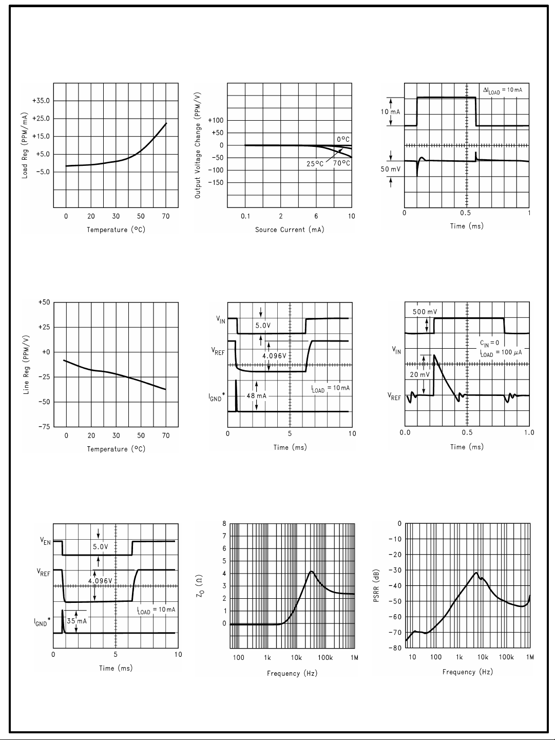
TYPICAL PERFORMANCE CURVES
Load Regulation vs Temperature
Line Regulation vs Temperature
Output Voltage vs Load Current
Power Up/Down Ground Current
Load Transient Response
Line Transient Response
Enable Response
Output Impedance
Power Supply Rejection Ratio
VRE4100DS REV. A MAY 01
 Loading...