

VRE4100 Series
Low Cost, SOIC-8
Precision References
THALER CORPORATION • 2015 N. FORBES BOULEVARD • TUCSON, AZ. 85745 • (520) 882-4000
FEATURES
• 1.024, 1.250, 2.048, 2.500, 4.096V Output
• Initial Error: ±0.05% max.
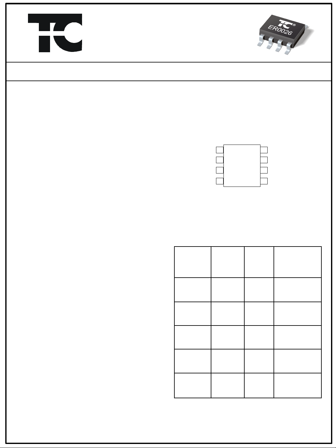
PIN CONFIGURATION
• Temperature Drift: 1.0 ppm/°C max.
• Low Noise: 2.2µV
(0.1Hz-10Hz, 1.024V)
p-p
• Low Thermal Hysterisis: 20ppm
• ±8mA Output Source
• Power Down Mode
• Industry Standard SOIC-8 pin out
• Commercial and Industrial Temp Ranges
• Second source for ADR29X, REF19X ,LT1460,
LT1461, LT1798, MAX616X, REF102
DESCRIPTION
The VRE4100 is a low cost, high precision
bandgap reference that operates from +5V. The
device features low noise, digital error correction,
and an SOIC-8 package. The ultrastable output
is 0.05% accurate with a temperature coefficient
as low as 1.0 ppm/°C. The improvement in
overall accuracy is made possible by using
EEPROM registers and CMOS DAC’s for
temperature and initial error correction. The DAC
trimming is done after assembly which eliminates
assembly related shifts.
The VRE4100 is recommended for use as a
reference for 14, 16, or 18 bit data converters
which require a precision reference. The
VRE4100 offers superior performance over
standard on-chip references commonly found
with data converters.
NC
+V
Enable
GND
1
VRE4100
2
IN
TOP
3
VIEW
4
8
NC
7
NC
6
V
REF
5
NC
FIGURE 1
SELECTION GUIDE
Output
Voltage
Model
VRE4110B 1.024 1.0 0°C to +70°C
VRE4110C 1.024 2.0 0°C to +70°C
VRE4110K 1.024 3.0 -40°C to +85°C
VRE4112B 1.250 1.0 0°C to +70°C
VRE4112C 1.250 2.0 0°C to +70°C
VRE4112K 1.250 3.0 -40°C to +85°C
VRE4120B 2.048 1.0 0°C to +70°C
VRE4120C 2.048 2.0 0°C to +70°C
VRE4120K 2.048 3.0 -40°C to +85°C
VRE4125B 2.500 1.0 0°C to +70°C
VRE4125C 2.500 2.0 0°C to +70°C
VRE4125K 2.500 3.0 -40°C to +85°C
VRE4141B 4.096 1.0 0°C to +70°C
VRE4141C 4.096 2.0 0°C to +70°C
VRE4141K 4.096 3.0 -40°C to +85°C
V
Temp.
Coeff.
ppm/°C
Temp.
Range °C
VRE4100DS REV. A MAY 01
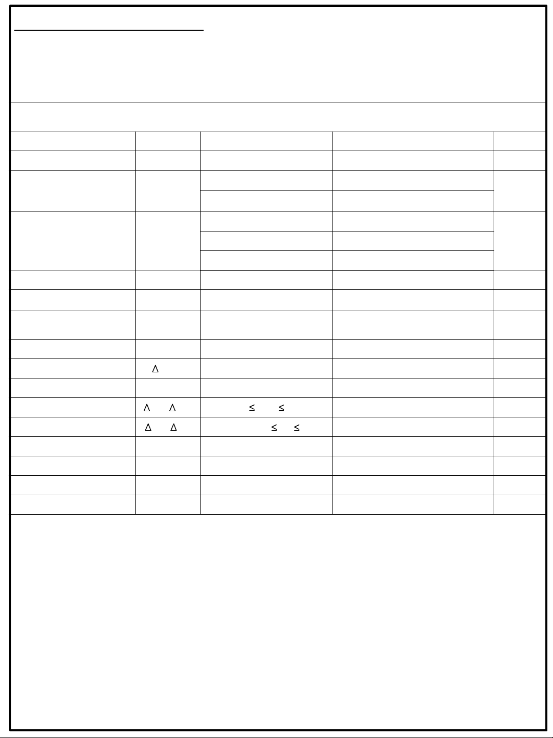
ABSOLUTE MAXIMUM RATINGS
Power supply to any input pin ….…-0.3V to +5.6V Output Short Circuit Duration …….…………....Indefinite
Operating Temp. (B,C) …………..……0°C to 70°C ESD Susceptibility Human Body Model…….…..…..2kV
Operating Temp. (K)………………...-40°C to 85°C ESD Susceptibility Machine Model ..………………200V
Storage Temperature Range……..-65°C to 150°C Lead Temperature (soldering,10 sec)………...….260°C
ELECTRICAL SPECIFICATIONS
Vps =+3V for VRE4110 and VRE4112, Vps =+5V for VRE4125, VRE4125 and VRE4141. T = 25°C, I
PARAMETER
=1mA, C
load
=1µF unless otherwise noted.
out
UNITSMIN TYP MAXSYMBOL CONDITIONS
Input Voltage
Output Voltage Error
(Note 1)
Output Voltage
Temperature Coefficient
(Note 2)
Dropout Voltage (Note 3)
Turn-On Settling Time
Output Noise Voltage
(Note 4)
Long Term Stability
Supply Current
Load Regulation (Note 6)
Line Regulation (Note 6)
Logic High Input Voltage
Logic High Input Current
Logic Low Input Voltage
Logic Low Input Current
IN
OUT
OUT
IN -VOUT
ON
n
OUT/T
IN
/ I
OUT
/ V
OUT
H
H
L
L
OUT
V1.8 5.5V
± 0.025% ± 0.050%VRE4100B
± 0.040% ± 0.080%VRE4100C/K
%V
0.5 1.0VRE4100B
1.0 2.0VRE4100C
ppm/°CTCV
1.5 3.0VRE4100K
160 235IL= 8 mA
mVV
µs2 To 0.01% of final valueT
µVp-p2.20.1Hz<f<10HzE
ppm20Note 5Temperature Hysterisis
ppm501000 HoursV
= 0mAI
load
8mAV
Load
IN
+ 200mV V
ref
IN
5.5VV
1 201mA I
µA230 320V
ppm/mA
ppm/V20 200V
V0.8V
nA2I
V0.4V
nA1I
Notes:
1. High temperature and mechanical stress can effect the initial accuracy of the VRE4100 series
references.See discussion on output accuracy.
2. The temperature coefficient is determined by the box method. See discussion on temperature
performance. All units are 100% tested over temperature.
3. The minimum input to output differential voltage at which the output voltage drops by 0.5% from nominal.
4. Based on 1.024V output. Noise is linearly proportional to V
REF.
5. Defined as change in 25°C output voltage after cycling device over operating temperature range.
6. Line and load regulation are measured with pulses and do not include output voltage changes due to self
heating.
VRE4100DS REV. A MAY 01
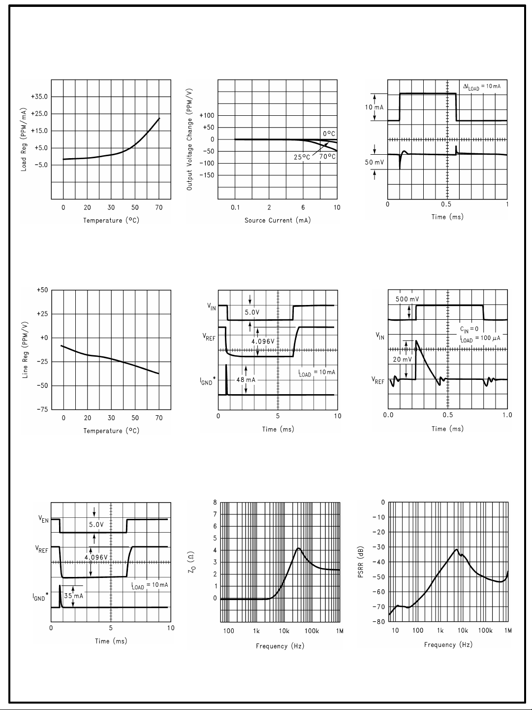
TYPICAL PERFORMANCE CURVES
Load Regulation vs Temperature
Line Regulation vs Temperature
Output Voltage vs Load Current
Power Up/Down Ground Current
Load Transient Response
Line Transient Response
Enable Response
Output Impedance
Power Supply Rejection Ratio
VRE4100DS REV. A MAY 01

TYPICAL PERFORMANCE CURVES
Total Current (Is
) vs Supply Voltage
(ON)
Output Voltage Change vs Sink Current I
(SINK)
Total Current (Is
) vs Supply Voltage
(OFF)
Dropout Voltage vs Load Current
Ground Current vs Load Current
IQvs Temperature
Dropout Voltage vs Load Current (V
) = 2.0V
OUT
Spectral Noise Density (0.1Hz to 10Hz)
Spectral Noise Density (10Hz to 100kHz)
VRE4100DS REV. A MAY 01

BASIC CIRCUIT CONNECTION
8 BIT
−
PIN DESCRIPTION
Figure 3 shows the proper connection of the
VRE4100 series voltage reference.
To achieve the specified performance, pay careful
attention to the layout. Commons should be
connected to a single point to minimize interconnect
resistances. This will reduce voltage errors, noise
pickup, and noise coupled from the power supply.
TEMPERATURE PERFORMANCE
The VRE4100 is designed for applications where
the initial error at room temperature and drift over
temperature are important to the user. For many
instrument manufacturers, a voltage reference with
a temperature coefficient of 1ppm/°C makes it
possible to eliminate a system temperature
calibration, a slow and costly process.
Of the three TC specification methods (slope,
butterfly, and box), the box method is most
commonly used. A box is formed by the min/max
limits for the nominal output voltage over the
operating temperature range. The equation follows:
VV
..
CT
=
alno
minmax
TTV
−
minmaxmin
6
)10(
)(
This method corresponds more accurately to the
method of test and provides a closer estimate of
actual error than the other methods. The box
method guarantees limits for the temperature error
but does not specify the exact shape or slope of the
device under test.
4
GND
These must be connected to
ground
2
Vin
Enable3
Positive power supply input
Pulled to Vinfor normal
operation.
This pin must be left openNC1,5,7,8
Reference outputVout6
+ V
NC
OUT
C
1µF
OUT
+ V
IN
Enable
2
3
6
VRE4100
1,5,7,8
4
Figure 2 External Connections
For example a designer who needs a 14-bit
accurate data acquisition system over the industrial
temperature range (-40°C to +85°C), will need a
voltage reference with a temperature coefficient
(TC) of 1.0ppm/°C if the reference is allowed to
contribute an error equivalent to 1LSB. Figure 3
shows the required reference TC vs. T change from
25°C for resolution ranging from 8 bits to 20 bits.
ReferenceTC
(ppm/°C)
Figure 3 Reference TC vs. T change from 25°C for 1 LSB change
10000
1000
100
10
1
0.1
0.01
1 10 100
10 BIT
12 BIT
14 BIT
16 BIT
18 BIT
20 BIT
VRE4100DS REV. A MAY 01

OPERATIONAL NOTES
Input Capacitor
An input capacitor is recommended on the VRE4100
device. A supply bypass capacitor on the input will
assure that the reference is working from a low
impedance source which will improve stability. It
can improve the transient response when the load
current is suddenly increased.
Output Capacitor
The VRE4100 requires a 1µF output capacitor for
loop stabilization (compensation) as well as
transient response. When the load current changes,
the output capacitor must source or sink current
during the time it takes the control loop of the
VRE4100 to respond.
The output capacitor must meet the requirements of
minimum capacitance and equivalent series
resistance (ESR) range. See Capacitor Selection
below.
Capacitor Selection
A minimum value of 0.2µF over the operating
temperature range is recommended. For a 0.22µF
capacitor the ESR range for 0°C -70°C is 0.9 to 6.0,
1.0µF is 0.8 to 6.0, and 10µF is 0.4 to 7.0.
Surface mount tantalum capacitors offer small size
for the value and ESR in the range required for the
VRE4100. The optimum performance for the output
capacitor is achieved with a 1.0µF value.
Aluminum electrolytic capacitors have a relatively
large size for the value. They meet the ESR
requirements at 1.0µF as long as the temperature is
above 0°C. Below 0°C, the ESR increases and it
may exceed the limits indicated in the figures.
Multilayer ceramic capacitors have a small size for
the value, are available in surface mount, and have
excellent RF characteristics. They may not meet the
minimum ESR requirements and have a large
change in value with temperature.
Reverse Current Path
ON/OFF Operation
The VRE4100 features a sleep mode that is
activated by pulling the enable pin low. To turn the
reference on, the enable pin is pulled high. If this
feature is not used, the the enable pin should be tied
to Vinto keep the reference on at all times. The
enable pin must not be left unconnected (floating).
When powered off, the VRE4100 will quickly reduce
both V
and IQ to zero. During power down, the
out
charge across the output capacitor is discharged to
ground through the internal circuitry. On power up,
the V
is restored in less than 200µs.
out
The signal source used to drive the enable pin can
come from either a totem-pole output or an open
collector output with a pull-up resistor to the
VRE4100 input voltage. The signal source must be
able to swing above and below the voltage
thresholds to guarantee an ON or OFF state. It
must not exceed the absolute maximum rating for
the enable pin.
Output Accuracy
The output accuracy after assembly at room
temperature is made up of three components: initial
accuracy of the device, thermal hysterisis, and
mechanical stress. The initial accuracy is measured
at the factory and may not reflect the actual output
voltage when the devices are mounted to a PCB.
The effects of mechanical stress and thermal
hysterisis can shift the output voltage.
Thermal Hysterisis
Thermal hysterisis is a change in output voltage
as a result of a temperature change. When
references experience a temperature change and
return to the initial temperature, they do not always
have the same initial voltage. Thermal hysterisis is
difficult to correct and is a major error source in
systems that experience temperature changes
greater than 25°C. Reference vendors are starting
to include this important specification in their
datasheets
The P-channel pass transistor used in the VRE4100
has an inherent diode connected between the V
and V
pins. Forcing the output to voltages higher
OUT
in
than the input or pulling Vinbelow the voltage stored
in the output capacitor by more than the Vbewill
forward bias this diode and current will flow from the
V
pin toVin. This will not damage the VRE4100 as
out
long as the current does not exceed 50mA.
Mechanical Hysterisis
Recommendations to minimize mechanical stress:
1) Mount the VRE4100 near the edges or corners of
the PCB. The center of the board generally has the
highest mechanical and thermal stress.
2) Mechanically isolate the device by cutting a U
shaped slot around the VRE4100. This provides
some mechanical and thermal isolation from the rest
of the circuit.
VRE4100DS REV. A MAY 01

MECHANICAL SPECIFICATIONSMECHANICAL SPECIFICATIONS
VRE4100DS REV. A MAY 01
 Loading...