

THALER VRE402LS, VRE402LD, VRE402KS, VRE402KD, VRE402JS Datasheet
...
VRE402
Precision
Dual Reference
DESCRIPTION
FEATURES
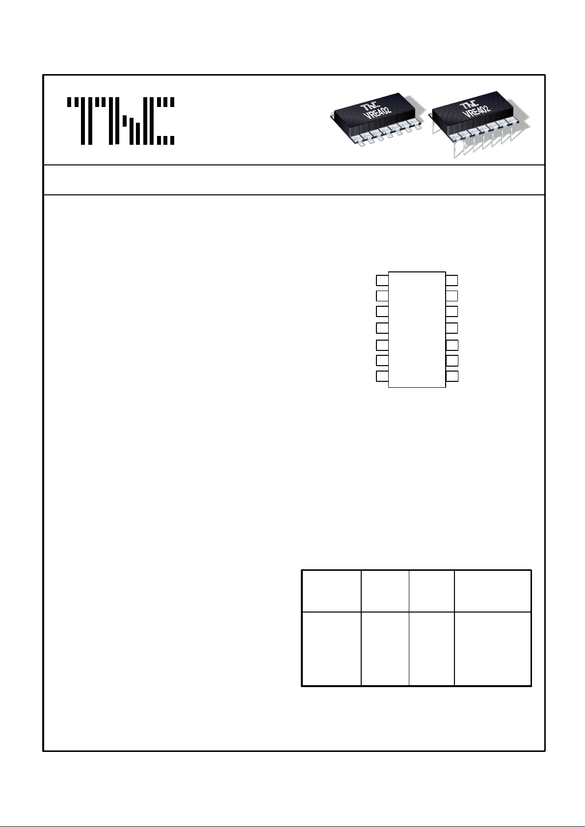
The VRE402 is a low cost, high precision, ±2.5V
reference. Packaged in 14 pin DIP or SMT
packages, the device is ideal for new designs that
need a high performance reference.
The device provides ultrastable ±2.500V output
with ±0.250 mV (.01%) initial accuracy and a
temperature coefficient of 0.6 ppm/°C. This
improvement in accuracy is made possible by a
unique, patented multipoint laser compensation
technique developed by Thaler Corporation.
Another key feature of this reference is the 0.3 mV
maximum tracking error between the positive and
negative output voltages over the operating
temperature range. This is extremely important in
high performance systems for reducing overall
system errors.
For designs which use the DIP package in a
socket, there is a reference ground pin to
eliminate reference ground errors.
The VRE402 is recommended for use as a
reference for high precision A/D and D/A
converters which require an external precision
reference. The device is ideal for calibrating
scale factor on high resolution A/D converters.
The VRE402 offers superior performance over
monolithic references.
• ±2.500 V OUTPUT ± 0.250 mV (.01%)
• TEMPERATURE DRIFT: 0.6 ppm/°C
• LOW NOISE: 1.5µVpp (0.1-10Hz)
• TRACKING ERROR: 0.2 mV max.
• EXCELLENT LINE REGULATION: 6ppm/V Typ.
• SURFACE MOUNT AND DIP PACKAGES
FIGURE 1
VRE402DS REV. A MAY 1996
SELECTION GUIDE
Model
Temp.
Range
°C
Temp.
Coeff.
ppm/
°C
VRE402A 0.25 0.6 0°C to +70°C
VRE402B 0.40 1.0 0°C to +70°C
VRE402C 0.50 2.0 0°C to +70°C
VRE402J 0.25 0.6 -40°C to +85°C
VRE402K 0.40 1.0 -40°C to +85°C
VRE402L 0.50 2.0 -40°C to +85°C
For package option add D for DIP or S for Surface
Mount to end of model number.
Initial
Error
mV
THALER CORPORATION • 2015 N. FORBES BOULEVARD • TUCSON, AZ. 85745 • (520) 882-4000
11
12
13
14
VRE402
TOP
VIEW
1
2
3
4
N/C
+V
IN
GND
REF. GND
+V
OUT
PIN CONFIGURATION
5
6
7
10
9
8
- V
OUT
N/C
- V
IN
N/C
N/C
N/C
N/C
N/C
N/C
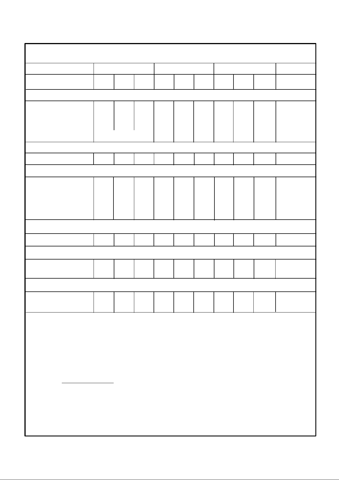
MODEL A/J B/K C/L
PARAMETER MIN TYP MAX MIN TYP MAX MIN TYP MAX UNITS
ABSOLUTE RATINGS
Power Supply ±13.5 ±15 ±22 * * * * * * V
Operating Temp. (A,B,C) 0 +70 * * * * °C
Operating Temp. (J,K,L) -40 +85 * * * * °C
Storage Temperature -65 +150 * * * * °C
Short Circuit Protection Continuous * *
OUTPUT VOLTAGE
VRE402 ±2.5 * * V
OUTPUT VOLTAGE ERRORS
Initial Error 0.25 0.40 0.50 mV
Warmup Drift 1 2 3 ppm
T
min
- T
max
0.6 1.0 2.0 ppm/ °C
Tracking Error 0.2 0.3 0.4 mV
Long-Term Stability 6 * * ppm/1000hrs
Noise (.1-10Hz) 1.5 * * µVpp
OUTPUT CURRENT
Range ±10 * * mA
REGULATION
Line 3 10 * * * * ppm/V
Load 3 * * ppm/mA
POWER SUPPLY CURRENTS
+PS 7 9 * * * * mA
-PS 4 6 * * * * mA
VRE402
NOTES: *Same as A/J Models.
1. The specified values are without external trim.
2. The temperature coefficient (tc) is determined by the
box method using the following formula:
V
max
- V
min
tc = x 10
6
V
nominal
x (T
max-Tmin
)
3. The tracking error is the deviation between the
positive and negative output over the operating temp.
range.
(1)
(4)
(2)
(3)
VRE402DS REV. A MAY 1996
Vps =±15V, T = 25°C, RL = 10KΩ unless otherwise noted.
ELECTRICAL SPECIFICATIONS
4. The specified values are unloaded.
 Loading...