

Page 1
T E X A S I N S T R U M E N T S
R F I D SYSTEMS
S P E C I F I C A T I O N
TRF79x0ATB
NFC/HF RFID Reader Module
Users Guide/Application Note
PRINTED COPIES OF THIS SPECIFICATION
ARE NOT CONTROLLED DOCUMENTS.
VERIFY THEIR CORRECT REVISION BEFORE USE.
Originator:
Joshua Wyatt
Revision: 0
Page 1 of 25
xx-xx-xx-xxx
Page 2

TI PROPRIETARY T E X A S I N S T R U M E N T S
INFORMATION -
Revision:
INTERNAL DATA R F I D SYSTEMS 0
S P E C I F I C A T I O N
TABLE OF CONTENTS PAGE
Purpose ................................................................................................................. 3
1.
2. Scope ..................................................................................................................... 3
3. References ............................................................................................................ 3
4. TRF79x0ATB Module Description ................................................................... 4
5. TRF79x0ATB Connections/Technical Details .................................................. 6
6. TRF79x0ATB Module Schematic ...................................................................... 7
7. MSP-EXP430F5438 Experimenters Board ...................................................... 8
8. DK-LM3S9B96-EM2-TRF7960R ARM Cortex M-3 Development Board . 10
9. Quick Start ........................................................................................................ 11
10. Base Application Firmware ............................................................................. 11
11. Platform Specific Details .................................................................................. 11
12. Mechanical/Physical Information .................................................................... 12
13. Antenna Tuning Details .................................................................................... 13
14. TRF79x0ATB Module Read Ranges ............................................................... 17
15. Revision History ................................................................................................ 18
Page 2 of 25
xx-xx-xx-xxx
Printed copies are not controlled documents - verify the correct revision before use.
Page 3

TI PROPRIETARY T E X A S I N S T R U M E N T S
INFORMATION -
Revision:
INTERNAL DATA R F I D SYSTEMS 0
S P E C I F I C A T I O N
1. Purpose
This document is intended to provide direction for TRF7960A/-70A users who desire to
implement a 13.56MHz NFC/RFID reader solution using the TRF79x0A IC connected to a
Texas Instruments embedded microcontroller or microprocessor development platform.
Examples of such development platforms are: the MSP-EXP430F5438 board, MSPEXP430F5529 board, the ARM Cortex-M3/M4 based board, or any other TI embedded
microcontroller platform with the EM socket headers populated.
2. Scope
This document will cover TRF79x0ATB module as it relates to using the module for
evaluation and development purposes in conjunction with Texas Instruments Embedded
Development platforms. This manual does not cover the in-depth details of the TRF79x0A
NFC/RFID IC families, as those details are well documented in the data sheets for those parts,
along with app notes that can be found on the product pages (see hyperlinks in References
section below).
3. References
TRF7960A Product Page: http://www.ti.com/product/trf7960A
TRF7970A Product Page: http://www.ti.com/product/trf7970A
TRF7960A Full Data Sheet: http://www.ti.com/lit/gpn/trf7960a
TRF7970A Full Data Sheet: http://www.ti.com/lit/gpn/trf7970a
TRF7960ATB Schematic, BOM and Design files: http://www.ti.com/litv/zip/sloc221
MSP-EXP430F5438 Users Guide: http://www.ti.com/lit/pdf/slau263
LM3S9B96 DK Users Guide: http://www.ti.com/litv/pdf/spmu036d
TPS61222DCKT Product Page: http://www.ti.com/product/tps61222
TI ISO15693/ISO18000-3 Inlays/Tags Parametric Search:
o http://focus.ti.com/paramsearch/docs/parametricsearch.tsp?family=rfid§ionId=4
75&tabId=2102&familyId=1352
Samtec Header and Mate Information:
Smith Chart Simulation Tool (licensed copy): http://www.fritz.dellsperger.net/
o https://www.samtec.com/ProductInformation/TechnicalSpecifications/Overview.aspx?series=SFM
o https://www.samtec.com/ProductInformation/TechnicalSpecifications/Overview.aspx?series=TFM
Page 3 of 25
xx-xx-xx-xxx
Printed copies are not controlled documents - verify the correct revision before use.
Page 4

TI PROPRIETARY T E X A S I N S T R U M E N T S
INFORMATION -
Revision:
INTERNAL DATA R F I D SYSTEMS 0
S P E C I F I C A T I O N
4. TRF79x0ATB Module(s) Description
The TRF79x0ATB Evaluation Modules are intended to allow the software application
developer to get familiar with the functionalities of either of the TRF79x0A MultiStandard Fully Integrated 13.56 MHz NFC/RFID reader ICs with the freedom to
develop on their Texas Instruments Embedded microcontroller development platform
of choice.
The TRF79x0ATB module is also intended to allow customer driven antenna tuning
with onboard coil and customer driven antenna form factor design.
The module is hard wired for SPI communications, supports Slave Select and
TRF79x0A Direct Mode 2 (default), Direct Mode 1 and Direct Mode 0 operations.
The user also has access to and full control over the TRF79x0A EN2 and EN lines,
allowing for design and development of ultra low power NFC/HF RFID systems.
The module has an onboard boost converter (TPS61222DCKT) which boosts
+3.3VDC in to +5VDC out to TRF79x0A IC for +23dBm (full transmitter power out)
operations.
An impedance matching circuit from 4Ω to 50Ω is populated on the module and this
is connected to a tuned 50Ω antenna circuit which consists of onboard four turn coil
with series and parallel passive elements (capacitors and a resistor).
Test points are available on the board for checking firmware operations with
oscilloscope or logic analyzer, impedance matching and for attaching external antenna.
Connection to Texas Instruments Microcontroller platforms are made via Samtec EM
headers located on the underside of the board (Connectors P1/RF1 and P2/RF2).
Page 4 of 25
xx-xx-xx-xxx
Printed copies are not controlled documents - verify the correct revision before use.
Page 5
TI PROPRIETARY T E X A S I N S T R U M E N T S
INFORMATION -
Revision:
INTERNAL DATA R F I D SYSTEMS 0
S P E C I F I C A T I O N
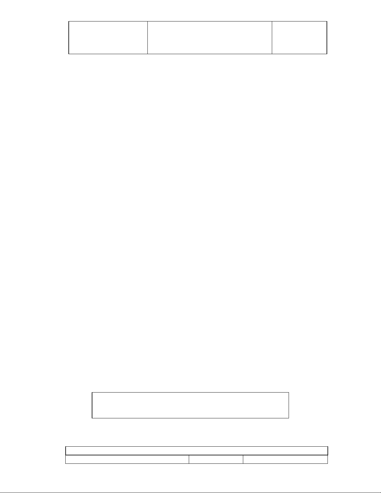
Figure 1: TRF7960ATB Evaluation Module
Figure 2: TRF7970ATB Evaluation Module
Page 5 of 25
xx-xx-xx-xxx
Printed copies are not controlled documents - verify the correct revision before use.
Page 6
TI PROPRIETARY T E X A S I N S T R U M E N T S
INFORMATION -
Revision:
INTERNAL DATA R F I D SYSTEMS 0
S P E C I F I C A T I O N
5. TRF79x0ATB Connections/Technical Details
Connector P1/RF1
Pin # Signal Name Description
1 GND Ground
2 n/c
3 MOD Direct mode, external modulation input
4 n/c
5 n/c
6 n/c
7 IRQ Interrupt request (from TRF79x0A to MCU)
8 n/c
9 SYS_CLK
10 EN Chip enable input (If EN = 0, then chip is in power-down mode).
11 n/c
12 EN2
13 n/c
14
15 n/c
16 DATA_CLK Data Clock Input for MCU Communication (from MCU)
17 n/c
18 MOSI I/O_7, Master Out, Slave In (Data In from MCU)
19 GND Ground
20 MISO I/O_6, Master In, Slave Out (Data Out from TRF7960)
SLAVE
SELECT
Pulse enable and selection of power down mode. If EN2 is connected to VIN, then
VDD_X is active during power down to support the MCU. Pin can also be used for
If EN = 0 and EN2 = 1, then system clock is set to 60 kHz
Clock for MCU (optional)
pulse wake-up from power-down mode.
Slave Select, I/O_4 (Active Low)
Connector P2/RF2
Pin # Signal Name Description
1 n/c
2 n/c
3 n/c
4 n/c
5 n/c
6 n/c
7 +3.3VDC IN +VDC in (to TPS61222DCKT for generation of +5VDC)
8 n/c
9 +3.3VDC IN +VDC in (to TPS61222DCKT for generation of +5VDC)
10 n/c
11 n/c
12 n/c
13 n/c
14 n/c
15 n/c
16 n/c
17 n/c
18 ASK/OOK
19 n/c
20 n/c
Direct mode, selection between ASK and OOK modulation (0 = ASK, 1 = OOK)
Also can be configured to provide the received analog signal output (ANA_OUT)
Page 6 of 25
xx-xx-xx-xxx
Printed copies are not controlled documents - verify the correct revision before use.
Page 7
TI PROPRIETARY T E X A S I N S T R U M E N T S
INFORMATION -
Revision:
INTERNAL DATA R F I D SYSTEMS 0
S P E C I F I C A T I O N
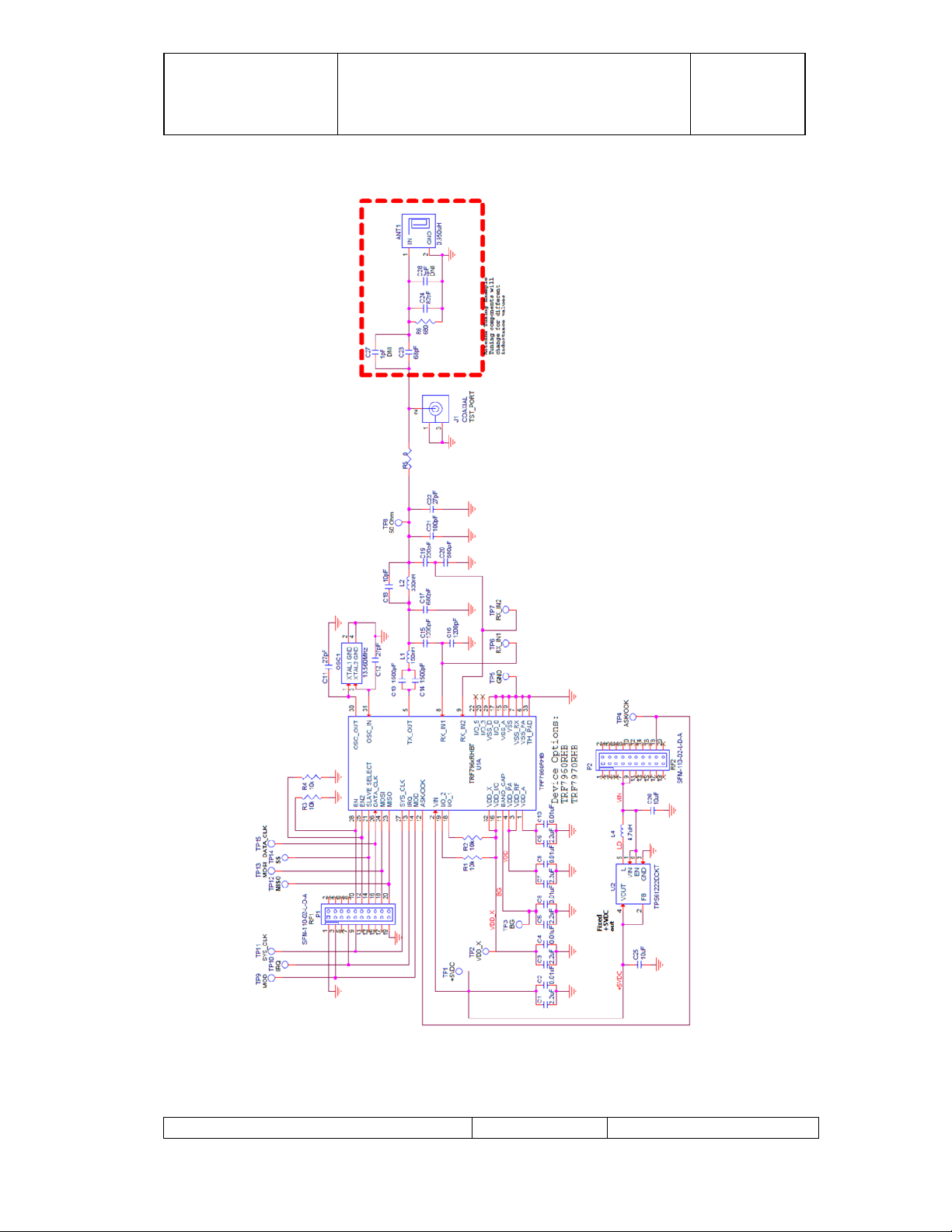
6. TRF79x0ATB Module Schematic
Note:
This schematic drives two separate layouts.
(TRF7960ATB.brd and TRF7970ATB.brd) the only difference is the bottom side silkscreen.
Page 7 of 25
xx-xx-xx-xxx
Printed copies are not controlled documents - verify the correct revision before use.
Page 8
TI PROPRIETARY T E X A S I N S T R U M E N T S
INFORMATION -
Revision:
INTERNAL DATA R F I D SYSTEMS 0
S P E C I F I C A T I O N
7. MSP-EXP430F5438 Experimenters Board
The MSP430F5438 Experimenter Board (MSP-EXP430F5438) is a development
platform for the latest generation MSP430 MCUs. It features a 100-pin socket which
supports the MSP430F5438 (datasheet) and other devices with similar pinouts. The
socket allows for quick upgrades to newer devices or quick applications changes. It is
also compatible with many TI low-power RF wireless evaluation modules such as the
CC2520EMK and the TRF79x0ATB module discussed here in this document.
The Experimenter Board helps designers quickly learn and develop using the new
F5xx MCUs, which provide the industry’s lowest active power consumption, more
memory and leading integration for applications such as energy harvesting, wireless
sensing and automatic metering infrastructure (AMI).
A TI Flash Emulation Tool, like the MSP-FET430UIF, is required to program and
debug the MSP430 devices on the experimenter board.
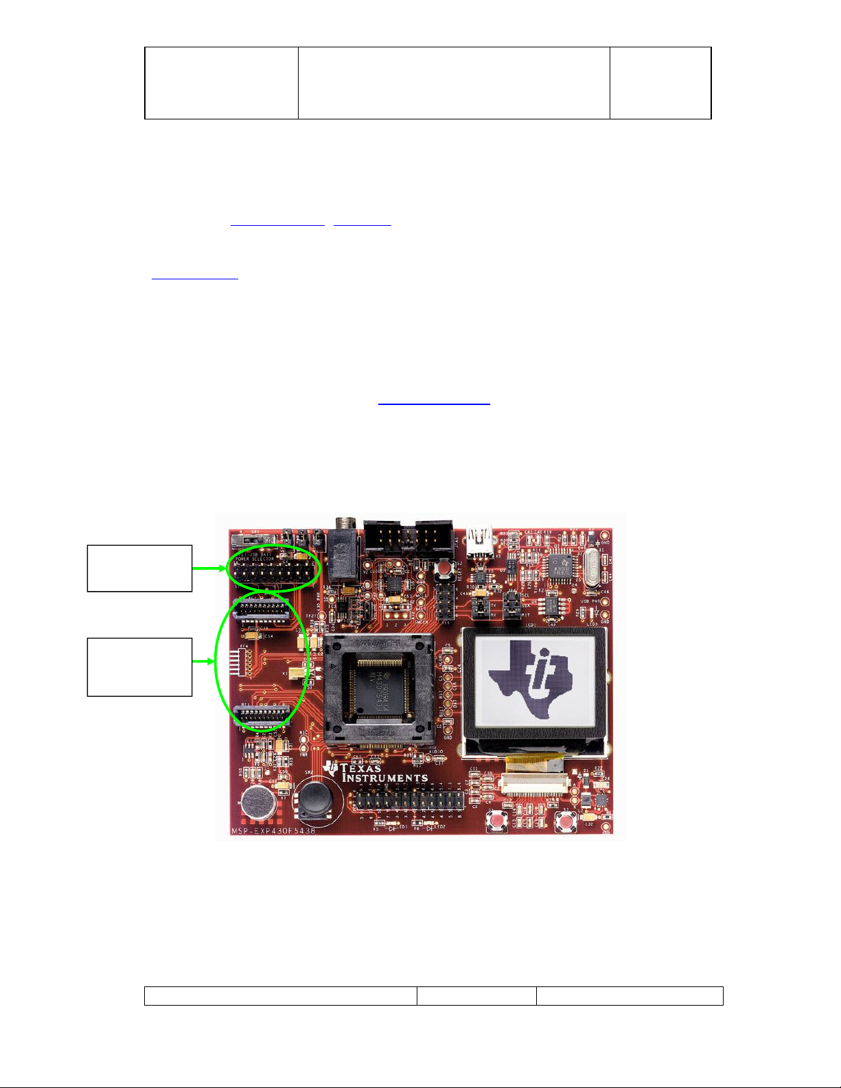
The TRF79x0ATB module plugs into the RF1 and RF2 headers on this MSP-EXP
board (see Figure 3). For logic analyzer connection during firmware debug, user can
use test points on TRF79x0ATB board or pins on header RF3.
RF3 Debug
Header
TRF79x0ATB
module
connects here
Figure 3: MSP-EXP430F5438 Development Board
Page 8 of 25
xx-xx-xx-xxx
Printed copies are not controlled documents - verify the correct revision before use.
Page 9
TI PROPRIETARY T E X A S I N S T R U M E N T S
INFORMATION -
Revision:
INTERNAL DATA R F I D SYSTEMS 0
S P E C I F I C A T I O N
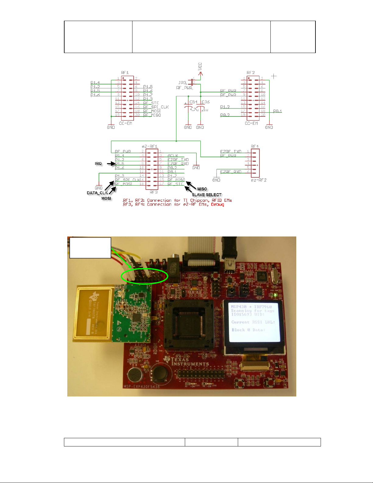
Figure 4: Debug Header (RF3) Logic Analyzer Connections for Monitoring SPI
communications between MSP430F5438A and TRF79x0A on TRF79x0ATB module
RF3 Debug
Header
Figure 5: Firmware Development\Debug Setup for
MSP-EXP430F5438 Experimenters Board
Page 9 of 25
xx-xx-xx-xxx
Printed copies are not controlled documents - verify the correct revision before use.
Page 10

TI PROPRIETARY T E X A S I N S T R U M E N T S
INFORMATION -
Revision:
INTERNAL DATA R F I D SYSTEMS 0
S P E C I F I C A T I O N
8. DK-LM3S9B96-EM2-TRF7960R ARM Cortex M-3 Development Board
The Stellaris DK-LM3S9B96-EM2-TRF7960R Development Kit provides a featurerich development platform for Ethernet, USB OTG/Host/Device, and CAN enabled
Stellaris ARM® Cortex™-M3-based microcontrollers. Each board has an In-Circuit
Debug Interface (ICDI) that provides hardware debugging functionality not only for
the on-board Stellaris devices, but also for any Stellaris microcontroller-based target
board. The development kit contains all cables, software, and documentation needed
to develop and run applications for Stellaris microcontrollers easily and quickly. The
Stellaris DK-LM3S9B96-EM2-TRF7960R Development Kit features: StellarisWare®
Peripheral Library, USB Library, and Graphics Library in conjunction with ARM
development tools from ARM tools partners. An EPI header to EM header interface
board (DK-LM3S9B96-EM2) is needed for use with the TRF7960TB module.
Figure 6: DK-LM3S9B96-EM2-TRF7960R Development Platform
Page 10 of 25
xx-xx-xx-xxx
Printed copies are not controlled documents - verify the correct revision before use.
Page 11

TI PROPRIETARY T E X A S I N S T R U M E N T S
INFORMATION -
Revision:
INTERNAL DATA R F I D SYSTEMS 0
S P E C I F I C A T I O N
9. Quick Start
1. Plug TRF79x0ATB Module into microcontroller development platform of
choice.
Note: if DK-LM3S9B96 board, remove SDRAM module and replace with
DK-LM3S9B96-EM2 interface board before attempting to mount
TRF79x0ATB module.
2. Apply power
3. Load base application firmware specific to platform working with.
4. Test for basic communication and functionality
5. Modify and Debug code as desired for specific application or protocol
6. Test for advanced functionality as implemented by modified code.
10. Base Application Firmware
TRF79x0ATB Module Base Application Firmware for various Texas
Instruments Microcontrollers and Microprocessors is available here:
MSP430F23xx:
http://www.ti.com/litv/zip/sloc203 (CCS or IAR)
MSP430F5438A: http://focus.ti.com/docs/toolsw/folders/print/msp-exp430f5438.html
LM3S9B96: http://focus.ti.com/docs/toolsw/folders/print/dk-lm3s9b96.html
11. Platform Specific Details
DK-LM3S9B96 Platform
o Mifare Specific Standalone Demo source code available
This code demonstrates (on up to two cards at a time)
MSP-EXP430F5438A Experimenters Board
o Code Example interfaces with standard TRF7960EVM GUI
http://www.ti.com/litv/zip/sloc134 (GUI)
http://www.ti.com/lit/pdf/slou192 (GUI Users Guide)
o ISO15693 UID & Block 0 Read/Automatic Product ID Demo
This code displays a single ISO15693 UID, RSSI Value
reading, authenticating and interacting with the Blocks
and Sectors of Mifare Classic 1k and 4k transponders.
& Block 0 Read/Automatic Product ID Demo on the
LCD. If more tags are in the field, or a different
protocol is desired, it requires use of the TRF7960 PC
based GUI to display multiple tags or interact with other
protocol based transponders.
Page 11 of 25
xx-xx-xx-xxx
Printed copies are not controlled documents - verify the correct revision before use.
Page 12

TI PROPRIETARY T E X A S I N S T R U M E N T S
INFORMATION -
Revision:
INTERNAL DATA R F I D SYSTEMS 0
S P E C I F I C A T I O N
12.
Mechanical/Physical Information
Page 12 of 25
xx-xx-xx-xxx
Printed copies are not controlled documents - verify the correct revision before use.
Page 13

TI PROPRIETARY T E X A S I N S T R U M E N T S
INFORMATION -
INTERNAL DATA R F I D SYSTEMS 0
S P E C I F I C A T I O N
13. Antenna Tuning Details
Module antenna as shipped is tuned for 50Ω impedance at 13.56MHz. It has a
nominal bandwidth of 1.3MHz, which results in a quality factor of
approximately 10. Module antenna circuit has a board mounted U.FL
connector installed for users that want to experiment with different tuning
solutions or disconnect onboard antenna and experiment with antennas of their
own design or application. Below are some design/application notes for users
to reference if they want to change the antenna Q factor or experiment further
on their own in order to serve their particular application directly.
TRF79x0ATB coil antenna tuning details starts with calculations to produce
the theoretical values shown below (and based on measurements of antenna
coil on Rev B board.) Coil value nominally measures 0.95uH at 13.56MHz
and
X
= 0.8 + j80.8 = 0.990 @ 63.4°.
L
To calculate the necessary values required for course resonance tuning and
proper Q setting of the antenna, the following formula is used.
1
)(
2
L
therefore;
C
totalRES
where ω = 2πf
Revision:
1
C
The dampening resistor value can now be calculated for a desired Q value
using the formula
therefore;
totalRES
)(
totalRES
)(
R
Q
PAR
fL
2
2
95.0)56.132(
pFC
157.145
HMHz
fLQR
PAR
Printed copies are not controlled documents - verify the correct revision before use.
2
Page 13 of 25
xx-xx-xx-xxx
Page 14

TI PROPRIETARY T E X A S I N S T R U M E N T S
INFORMATION -
INTERNAL DATA R F I D SYSTEMS 0
S P E C I F I C A T I O N
For Q = ~20 (ISO15693 operations):
kR
PAR
(move to standard value of 1.3kΩ)
For Q = ~10 (ISO14443 and ISO15693 operations):
29.1
Revision:
R
PAR
(move to standard value of 680Ω)
Smith Chart simulation for R
capacitor values capacitor values to be 97pF and 51pF, respectively.
(This is < +2% change from the calculated total cap value.)
Smith Chart simulation for R
parallel and series capacitor values to be 82pF and 69pF, respectively.
(This is < +4% change from the calculated value.)
value = 1.3kΩ reveals theoretical parallel and series
PAR
value = 680Ω (standard value) reveals theoretical
PAR
647
Printed copies are not controlled documents - verify the correct revision before use.
Page 14 of 25
xx-xx-xx-xxx
Page 15
TI PROPRIETARY T E X A S I N S T R U M E N T S
INFORMATION -
Revision:
INTERNAL DATA R F I D SYSTEMS 0
S P E C I F I C A T I O N
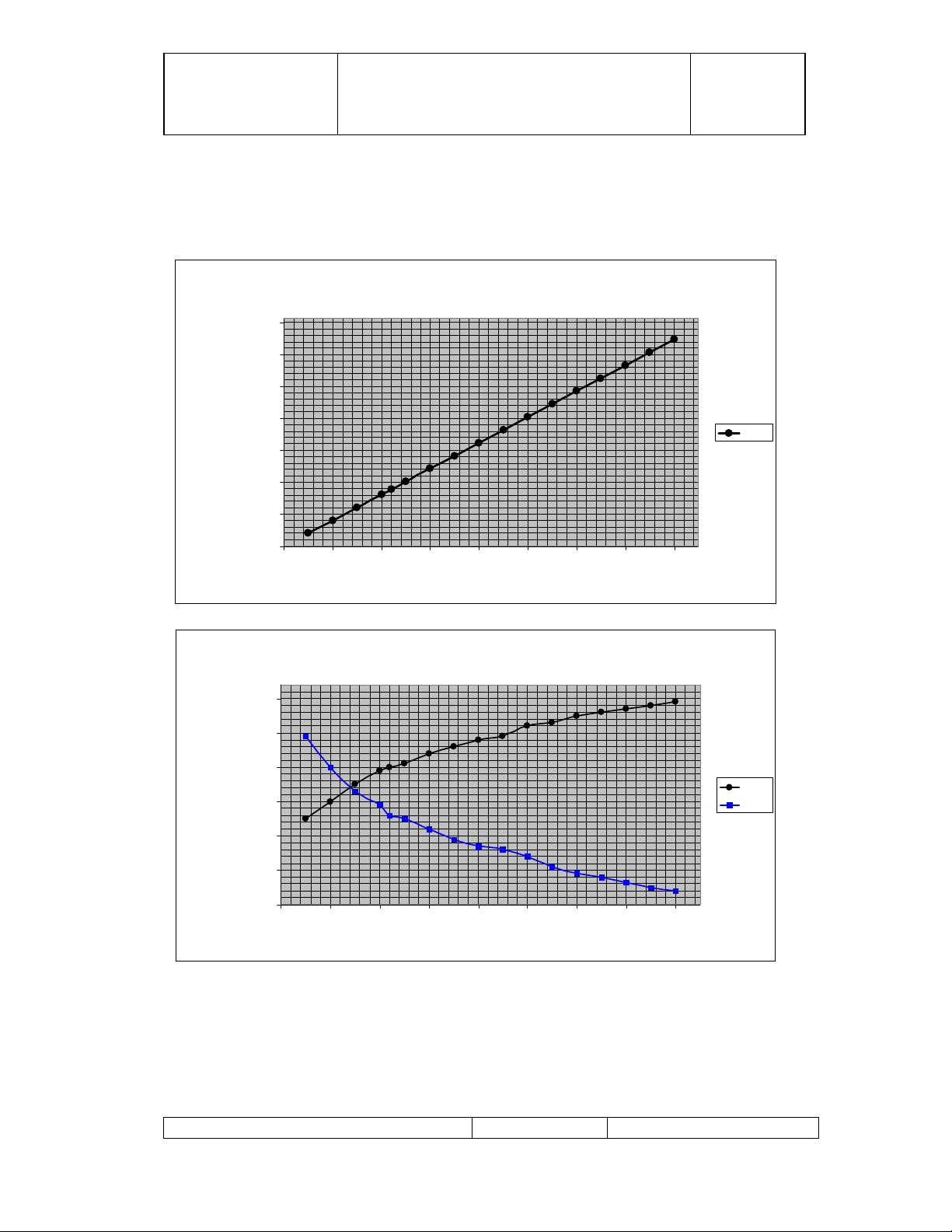
The calculations and simulations for a desired Q range of 5 to 20 results in the
following diagrams which indicate the required resistor and capacitance values
should be populated.
Theoretical P arallel Resistor V al ue for Desired Q
001.73E+03
001.53E+03
001.33E+03
001.13E+03
Ohms
925.00E+00
725.00E+00
525.00E+00
325.00E+00
102.00E-12
092.00E-12
082.00E-12
072.00E-12
062.00E-12
Capacitance (in pF)
052.00E-12
1.30E+03
680.71E+00
4 6 8 10 12 14 16 18 20
Q Value
Theoretical Capacitance Values for Resonance at Desired Q
97.00E-12
82.00E-12
68.00E-12
51.00E-12
Rpar
Cpar
Cser
042.00E-12
4 6 8 10 12 14 16 18 20
Q
Page 15 of 25
xx-xx-xx-xxx
Printed copies are not controlled documents - verify the correct revision before use.
Page 16
TI PROPRIETARY T E X A S I N S T R U M E N T S
INFORMATION -
Revision:
INTERNAL DATA R F I D SYSTEMS 0
S P E C I F I C A T I O N
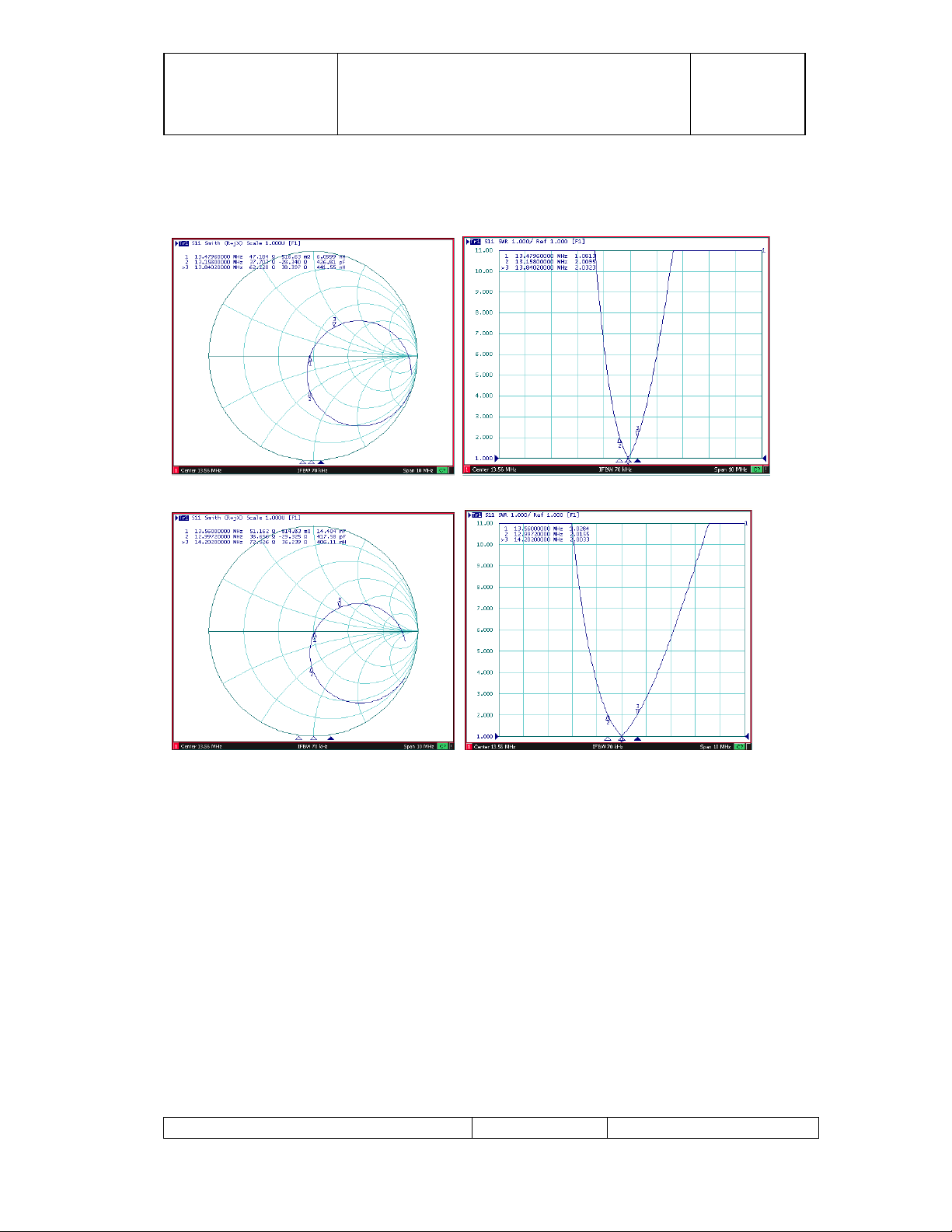
Actual measurements on TRF79x0ATB module for high and lower Q value
tuning solutions.
Higher Q Antenna Measurement Plots with Calculated Values (Q = ~20)
Lower Q Antenna Measurement Plots with Calculated Valu es (Q = ~10)
Page 16 of 25
xx-xx-xx-xxx
Printed copies are not controlled documents - verify the correct revision before use.
Page 17
TI PROPRIETARY T E X A S I N S T R U M E N T S
INFORMATION -
Revision:
INTERNAL DATA R F I D SYSTEMS 0
S P E C I F I C A T I O N
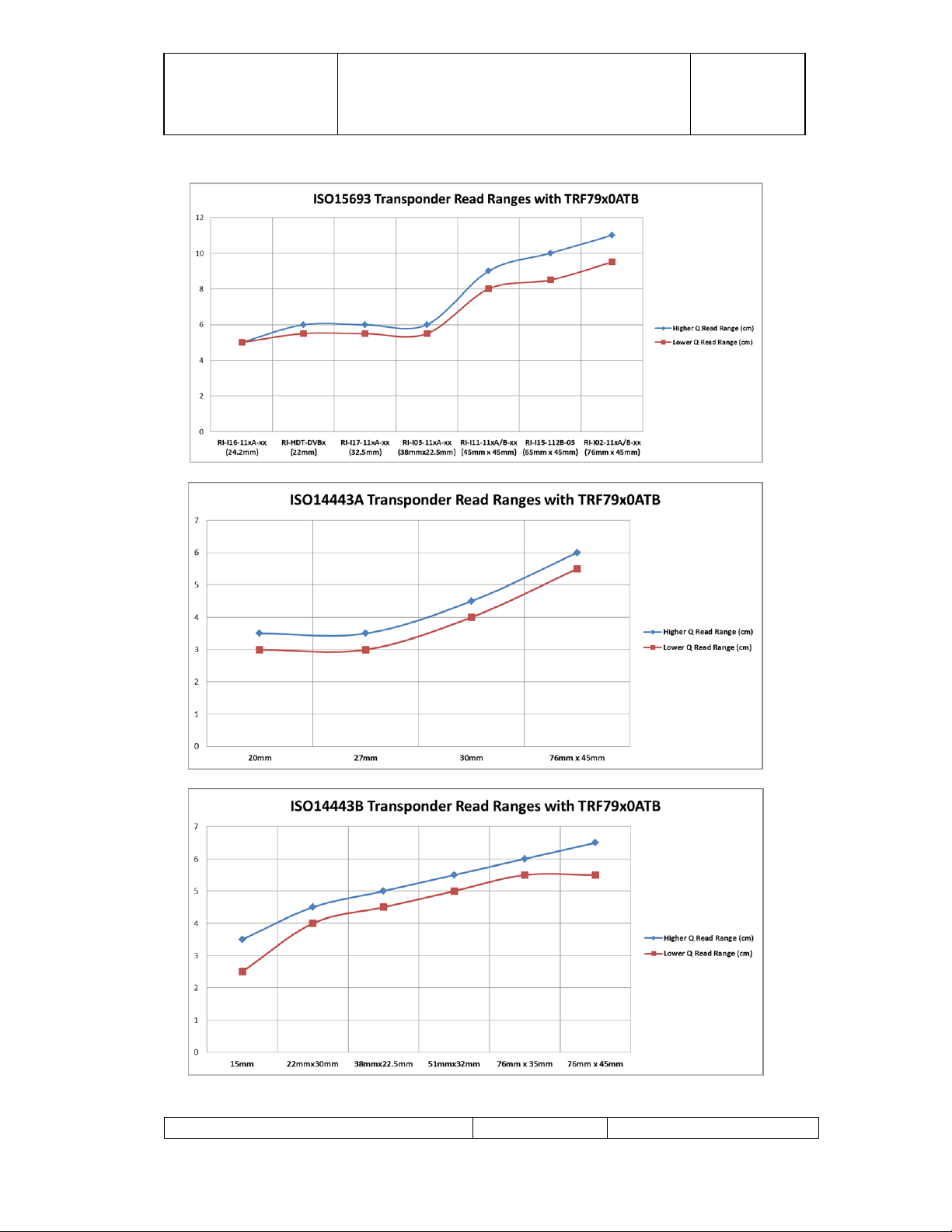
14. TRF79x0ATB Module Read Ranges
Page 17 of 25
xx-xx-xx-xxx
Printed copies are not controlled documents - verify the correct revision before use.
Page 18

TI PROPRIETARY T E X A S I N S T R U M E N T S
INFORMATION -
Revision:
INTERNAL DATA R F I D SYSTEMS 0
S P E C I F I C A T I O N
15. Revision History
Version SCN Description of Change Date submitted By
Rev.
0 0 New Issue 04/18/2013 Joshua Wyatt
Page 18 of 25
xx-xx-xx-xxx
Printed copies are not controlled documents - verify the correct revision before use.
Page 19

TI PROPRIETARY T E X A S I N S T R U M E N T S
INFORMATION -
Revision:
INTERNAL DATA R F I D SYSTEMS 0
S P E C I F I C A T I O N
EVALUATION BOARD/KIT/MODULE (EVM) ADDITIONAL TERMS
Texas Instruments (TI) provides the enclosed Evaluation Board/Kit/Module
(EVM) under the following conditions:
The user assumes all responsibility and liability for proper and safe handling
of the goods. Further, the user indemnifies TI from all claims arising from the
handling or use of the goods.
Should this evaluation board/kit not meet the specifications indicated in the
User’s Guide, the board/ kit may be returned within 30 days from the date of
delivery for a full refund. THE FOREGOING LIMITED WARRANTY IS
THE EXCLUSIVE WARRANTY MADE BY SELLER TO BUYER AND IS
IN LIEU OF ALL OTHER WARRANTIES, EXPRESSED, IMPLIED, OR
STATUTORY, INCLUDING ANY WARRANTY OF
MERCHANTABILITY OR FITNESS FOR ANY PARTICULAR PURPOSE.
EXCEPT TO THE EXTENT OF THE INDEMNITY SET FORTH ABOVE,
NEITHER PARTY SHALL BE LIABLE TO THE OTHER FOR ANY
INDIRECT, SPECIAL, INCIDENTAL, OR CONSEQUENTIAL
DAMAGES.
Please read the User's Guide and, specifically, the Warnings and Restrictions
notice in the User's Guide prior to handling the product. This notice contains
important safety information about temperatures and voltages. For additional
information on TI's environmental and/or safety programs, please visit
www.ti.com/esh or contact TI.
No license is granted under any patent right or other intellectual property right
of TI covering or relating to any machine, process, or combination in which
such TI products or services might be or are used. TI currently deals with a
variety of customers for products, and therefore our arrangement with the user
is not exclusive. TI assumes no liability for applications assistance, customer
product design, software performance, or infringement of patents or services
described herein.
Mailing Address:
Texas Instruments Post Office Box 655303 Dallas, Texas 75265
Copyright 2011, Texas Instruments Incorporated
Page 19 of 25
xx-xx-xx-xxx
Printed copies are not controlled documents - verify the correct revision before use.
Page 20

TI PROPRIETARY T E X A S I N S T R U M E N T S
INFORMATION -
Revision:
INTERNAL DATA R F I D SYSTEMS 0
S P E C I F I C A T I O N
REGULATORY COMPLIANCE INFORMATION
As noted in the EVM User’s Guide and/or EVM itself, this EVM and/or
accompanying hardware may or may not be subject to the Federal
Communications Commission (FCC) and Industry Canada (IC) rules.
For EVMs not subject to the above rules, this evaluation board/kit/module is
intended for use for ENGINEERING DEVELOPMENT, DEMONSTRATION
OR EVALUATION PURPOSES ONLY and is not considered by TI to be a
finished end product fit for general consumer use. It generates, uses, and can
radiate radio frequency energy and has not been tested for compliance with the
limits of computing devices pursuant to part 15 of FCC or ICES-003 rules,
which are designed to provide reasonable protection against radio frequency
interference. Operation of the equipment may cause interference with radio
communications, in which case the user at his own expense will be required to
take whatever measures may be required to correct this interference.
General Statement for EVMs including a radio
User Power/Frequency Use Obligations: This radio is intended for
development/professional use only in legally allocated frequency and power
limits. Any use of radio frequencies and/or power availability of this EVM and
its development application(s) must comply with local laws governing radio
spectrum allocation and power limits for this evaluation module. It is the
user’s sole responsibility to only operate this radio in legally acceptable
frequency space and within legally mandated power limitations. Any
exceptions to this is strictly prohibited and unauthorized by Texas Instruments
unless user has obtained appropriate experimental/development licenses from
local regulatory authorities, which is responsibility of user including its
acceptable authorization.
Page 20 of 25
xx-xx-xx-xxx
Printed copies are not controlled documents - verify the correct revision before use.
Page 21

TI PROPRIETARY T E X A S I N S T R U M E N T S
INFORMATION -
Revision:
INTERNAL DATA R F I D SYSTEMS 0
S P E C I F I C A T I O N
For EVMs annotated as FCC – FEDERAL COMMUNICATIONS
COMMISSION Part 15 Compliant
Caution
This device complies with part 15 of the FCC Rules. Operation is subject to
the following two conditions: (1) This device may not cause harmful
interference, and (2) this device must accept any interference received,
including interference that may cause undesired operation.
Changes or modifications not expressly approved by the party responsible for
compliance could void the user's authority to operate the equipment.
FCC Interference Statement for Class A EVM devices
This equipment has been tested and found to comply with the limits for a
Class A digital device, pursuant to part 15 of the FCC Rules. These limits are
designed to provide reasonable protection against harmful interference when
the equipment is operated in a commercial environment. This equipment
generates, uses, and can radiate radio frequency energy and, if not installed
and used in accordance with the instruction manual, may cause harmful
interference to radio communications. Operation of this equipment in a
residential area is likely to cause harmful interference in which case the user
will be required to correct the interference at his own expense.
FCC Interference Statement for Class B EVM devices
This equipment has been tested and found to comply with the limits for a
Class B digital device, pursuant to part 15 of the FCC Rules. These limits are
designed to provide reasonable protection against harmful interference in a
residential installation. This equipment generates, uses and can radiate radio
frequency energy and, if not installed and used in accordance with the
instructions, may cause harmful interference to radio communications.
However, there is no guarantee that interference will not occur in a particular
installation. If this equipment does cause harmful interference to radio or
television reception, which can be determined by turning the equipment off
and on, the user is encouraged to try to correct the interference by one or more
of the following measures:
Reorient or relocate the receiving antenna.
Increase the separation between the equipment and receiver.
Connect the equipment into an outlet on a circuit different from that to which
the receiver is connected.
Consult the dealer or an experienced radio/TV technician for help.
Page 21 of 25
xx-xx-xx-xxx
Printed copies are not controlled documents - verify the correct revision before use.
Page 22

TI PROPRIETARY T E X A S I N S T R U M E N T S
INFORMATION -
Revision:
INTERNAL DATA R F I D SYSTEMS 0
S P E C I F I C A T I O N
For EVMs annotated as IC – INDUSTRY CANADA Compliant
This Class A or B digital apparatus complies with Canadian ICES-003.
Changes or modifications not expressly approved by the party responsible for
compliance could void the user’s authority to operate the equipment.
Concerning EVMs including radio transmitters
This device complies with Industry Canada licence-exempt RSS standard(s).
Operation is subject to the following two conditions: (1) this device may not
cause interference, and (2) this device must accept any interference, including
interference that may cause undesired operation of the device.
Concerning EVMs including detachable antennas
Under Industry Canada regulations, this radio transmitter may only operate
using an antenna of a type and maximum (or lesser) gain approved for the
transmitter by Industry Canada. To reduce potential radio interference to other
users, the antenna type and its gain should be so chosen that the equivalent
isotropically radiated power (e.i.r.p.) is not more than that necessary for
successful communication.
This radio transmitter has been approved by Industry Canada to operate with
the antenna types listed in the user guide with the maximum permissible gain
and required antenna impedance for each antenna type indicated. Antenna
types not included in this list, having a gain greater than the maximum gain
indicated for that type, are strictly prohibited for use with this device.
~
Cet appareil numérique de la classe A ou B est conforme à la norme NMB-003
du Canada.
Les changements ou les modifications pas expressément approuvés par la
partie responsable de la conformité ont pu vider l’autorité de l'utilisateur pour
actionner l'équipement.
Concernant les EVMs avec appareils radio
Le présent appareil est conforme aux CNR d'Industrie Canada applicables aux
appareils radio exempts de licence. L'exploitation est autorisée aux deux
conditions suivantes : (1) l'appareil ne doit pas produire de brouillage, et (2)
l'utilisateur de l'appareil doit accepter tout brouillage radioélectrique subi,
même si le brouillage est susceptible d'en compromettre le fonctionnement.
Concernant les EVMs avec antennes détachables
Conformément à la réglementation d'Industrie Canada, le présent émetteur
radio peut fonctionner avec une antenne d'un type et d'un gain maximal (ou
inférieur) approuvé pour l'émetteur par Industrie Canada. Dans le but de
réduire les risques de brouillage radioélectrique à l'intention des autres
utilisateurs, il faut choisir le type d'antenne et son gain de sorte que la
Page 22 of 25
xx-xx-xx-xxx
Printed copies are not controlled documents - verify the correct revision before use.
Page 23

TI PROPRIETARY T E X A S I N S T R U M E N T S
INFORMATION -
Revision:
INTERNAL DATA R F I D SYSTEMS 0
S P E C I F I C A T I O N
puissance isotrope rayonnée équivalente (p.i.r.e.) ne dépasse pas l'intensité
nécessaire à l'établissement d'une communication satisfaisante.
Le présent émetteur radio a été approuvé par Industrie Canada pour
fonctionner avec les types d'antenne énumérés dans le manuel d’usage et ayant
un gain admissible maximal et l'impédance requise pour chaque type
d'antenne. Les types d'antenne non inclus dans cette liste, ou dont le gain est
supérieur au gain maximal indiqué, sont strictement interdits pour
l'exploitation de l'émetteur.
【Important Notice for Users of this Product in Japan】
This development kit is NOT certified as Confirming to Technical
Regulations of Radio Law of Japan!
If you use this product in Japan, you are required by Radio Law of Japan to
follow the instructions below with respect to this product:
(1) Use this product in a shielded room or any other test facility as defined in
the notification #173 issued by Ministry of Internal Affairs and
Communications on March 28, 2006, based on Sub-section 1.1 of Article 6 of
the Ministry’s Rule for Enforcement of Radio Law of Japan,
(2) Use this product only after you obtained the license of Test Radio Station
as provided in Radio Law of Japan with respect to this product, or
(3) Use of this product only after you obtained the Technical Regulations
Conformity Certification as provided in Radio Law of Japan with respect to
this product.
Also, please do not transfer this product, unless you give the same notice
above to the transferee.
Please note that if you could not follow the instructions above, you will be
subject to penalties of Radio Law of Japan.
Texas Instruments Japan Limited
24-1, Nishi-Shinjuku 6 chome, Shinjukku-ku, Tokyo, Japan
http://www.tij.co.jp
【ご使用にあたっての注意】
本開発キットは技術基準適合証明を受けておりません。
本製品のご使用に際しては、電波法遵守のため、以下のいずれかの措
置を取っていただく必要がありますのでご注意ください。
(1)電波法施行規則第 6 条第 1 項第 1 号に基づく平成 18 年 3 月 28
日総務省告示第 173 号で定められた電波暗室等の試験設備でご使用い
ただく。
(2)実験局の免許を取得後ご使用いただく。
(3)技術基準適合証明を取得後ご使用いただく。
なお、本製品は、上記の「ご使用にあたっての注意」を譲渡先、移転
先に通知しない限り、譲渡、移転できないものとします。
Page 23 of 25
xx-xx-xx-xxx
Printed copies are not controlled documents - verify the correct revision before use.
Page 24

TI PROPRIETARY T E X A S I N S T R U M E N T S
INFORMATION -
Revision:
INTERNAL DATA R F I D SYSTEMS 0
S P E C I F I C A T I O N
上記を遵守頂けない場合は、電波法の罰則が適用される可能性がある
ことをご留意ください。
日本テキサス・インスツルメンツ株式会社
東京都新宿区西新宿6丁目24番1号
西新宿三井ビル
http://www.tij.co.jp
EVALUATION BOARD/KIT/MODU LE (EVM)
WARNINGS, RESTRICTIONS AND DISCLAIMERS
For Feasibility Evaluation Only, in Laboratory/Development
Environments. Unless otherwise indicated, this EVM is not a finished
electrical equipment and not intended for consumer use. It is intended solely
for use for preliminary feasibility evaluation in laboratory/development
environments by technically qualified electronics experts who are familiar
with the dangers and application risks associated with handling electrical
mechanical components, systems and subsystems. It should not be used as all
or part of a finished end product.
Your Sole Responsibility and Risk. You acknowledge, represent and agree
that:
1. You have unique knowledge concerning Federal, State and local
regulatory requirements (including but not limited to Food and Drug
Administration regulations, if applicable) which relate to your products
and which relate to your use (and/or that of your employees, affiliates,
contractors or designees) of the EVM for evaluation, testing and other
purposes.
2. You have full and exclusive responsibility to assure the safety and
compliance of your products with all such laws and other applicable
regulatory requirements, and also to assure the safety of any activities
to be conducted by you and/or your employees, affiliates, contractors
or designees, using the EVM. Further, you are responsible to assure
that any interfaces (electronic and/or mechanical) between the EVM
and any human body are designed with suitable isolation and means to
safely limit accessible leakage currents to minimize the risk of
electrical shock hazard.
3. You will employ reasonable safeguards to ensure that your use of the
EVM will not result in any property damage, injury or death, even if
the EVM should fail to perform as described or expected.
4. You will take care of proper disposal and recycling of the EVM’s
electronic components and packing materials
Page 24 of 25
xx-xx-xx-xxx
Printed copies are not controlled documents - verify the correct revision before use.
Page 25

TI PROPRIETARY T E X A S I N S T R U M E N T S
INFORMATION -
Revision:
INTERNAL DATA R F I D SYSTEMS 0
S P E C I F I C A T I O N
Certain Instructions. It is important to operate this EVM within TI’s
recommended specifications and environmental considerations per the user
guidelines. Exceeding the specified EVM ratings (including but not limited to
input and output voltage, current, power, and environmental ranges) may
cause property damage, personal injury or death. If there are questions
concerning these ratings please contact a TI field representative prior to
connecting interface electronics including input power and intended loads.
Any loads applied outside of the specified output range may result in
unintended and/or inaccurate operation and/or possible permanent damage to
the EVM and/or interface electronics. Please consult the EVM User's Guide
prior to connecting any load to the EVM output. If there is uncertainty as to
the load specification, please contact a TI field representative. During normal
operation, some circuit components may have case temperatures greater than
60 C as long as the input and output are maintained at a normal ambient
operating temperature. These components include but are not limited to linear
regulators, switching transistors, pass transistors, and current sense resistors
which can be identified using the EVM schematic located in the EVM User's
Guide. When placing measurement probes near these devices during normal
operation, please be aware that these devices may be very warm to the touch.
As with all electronic evaluation tools, only qualified personnel
knowledgeable in electronic measurement and diagnostics normally found in
development environments should use these EVMs
Agreement to Defend, Indemnify and Hold Harmless. You agree to defend,
indemnify and hold TI, its licensors and their representatives harmless from
and against any and all claims, damages, losses, expenses, costs and liabilities
(collectively, "Claims") arising out of or in connection with any use of the
EVM that is not in accordance with the terms of the agreement. This
obligation shall apply whether Claims arise under law of tort or contract or any
other legal theory, and even if the EVM fails to perform as described or
expected.
Safety-Critical or Life-Critical Applications. If you intend to evaluate the
components for possible use in safety critical applications (such as life
support) where a failure of the TI product would reasonably be expected to
cause severe personal injury or death, such as devices which are classified as
FDA Class III or similar classification, then you must specifically notify TI of
such intent and enter into a separate Assurance and Indemnity Agreement.
Page 25 of 25
xx-xx-xx-xxx
Printed copies are not controlled documents - verify the correct revision before use.
 Loading...