

Page 1

TI Confidential – NDA Restrictions
CC3235MODSF SimpleLink™ Wi-Fi®and IoT Solution With MCU LaunchPad™ Hardware
User's Guide
Literature Number: SWRU548A
February 2019
Page 2

TI Confidential – NDA Restrictions
Contents
1 Introduction......................................................................................................................... 6
1.1 CC3235MODSF LaunchPad™ ........................................................................................ 6
1.2 LAUNCHCC3235MOD Key Features ................................................................................. 7
1.3 What's Included .......................................................................................................... 7
1.4 REACH Compliance ..................................................................................................... 7
1.5 Regulatory Compliance ................................................................................................. 8
1.6 First Steps: Out-of-Box Experience ................................................................................... 8
1.7 Next Steps: Looking into the Provided Code ........................................................................ 8
1.8 Trademarks ............................................................................................................... 9
2 Hardware .......................................................................................................................... 10
2.1 Block Diagram........................................................................................................... 11
2.2 Hardware Features ..................................................................................................... 13
2.3 Electrical Characteristics .............................................................................................. 27
2.4 Antenna Characteristics ............................................................................................... 27
2.5 BoosterPack™ Header Pin Assignment ............................................................................ 28
3 Layout Guidelines .............................................................................................................. 29
3.1 LAUNCHCC3235MOD Board Layout ................................................................................ 29
3.2 General Layout Recommendations .................................................................................. 33
3.3 RF Layout Recommendations ........................................................................................ 33
3.4 Antenna Placement and Routing .................................................................................... 35
3.5 Transmission Line Considerations ................................................................................... 35
4 Operational Setup and Testing ............................................................................................ 37
4.1 Measuring the CC3235MOD Current Draw ........................................................................ 38
4.2 RF Connections ........................................................................................................ 39
4.3 Design Files ............................................................................................................ 40
4.4 Software ................................................................................................................. 40
5 Development Environment Requirements ............................................................................. 40
5.1 CCS ...................................................................................................................... 40
5.2 IAR........................................................................................................................ 40
6 Additional Resources ......................................................................................................... 41
6.1 CC3235MODx Product Page ......................................................................................... 41
6.2 Download CCS, IAR ................................................................................................... 41
6.3 SimpleLink™ Academy for CC3235 SDK .......................................................................... 41
6.4 TI E2E Community ..................................................................................................... 41
7 Assembly Drawing and Schematics ..................................................................................... 42
7.1 Assembly Drawing ..................................................................................................... 42
7.2 Schematics ............................................................................................................. 43
Revision History.......................................................................................................................... 48
1 ........................................................................................................................................ 49
2 RF Function and Frequency Range....................................................................................... 49
3 FCC and IC Certification and Statement ................................................................................ 49
2
Table of Contents
Copyright © 2019, Texas Instruments Incorporated
SWRU548A–February 2019
Submit Documentation Feedback
Page 3

TI Confidential – NDA Restrictions
www.ti.com
3.1 FCC....................................................................................................................... 49
3.2 CAN ICES-3(B) and NMB-3(B) Certification and Statement...................................................... 50
3.3 End Product Labeling .................................................................................................. 51
3.4 Device Classifications.................................................................................................. 51
3.5 FCC Definitions ......................................................................................................... 51
3.6 Simultaneous Transmission Evaluation.............................................................................. 52
4 EU Certification and Statement ............................................................................................ 52
4.1 RF Exposure Information (MPE)...................................................................................... 52
4.2 Simplified DoC Statement ............................................................................................. 52
4.3 Waste Electrical and Electronic Equipment (WEEE)............................................................... 53
4.4 OEM and Host Manufacturer Responsibilities ...................................................................... 53
4.5 Antenna Specifications................................................................................................. 53
5 CC3235MODx Approved Antennas ....................................................................................... 53
SWRU548A–February 2019
Submit Documentation Feedback
Copyright © 2019, Texas Instruments Incorporated
Contents
3
Page 4

TI Confidential – NDA Restrictions
User's Guide
SWRU548A–February 2019
CC3235MODSF LaunchPad™ Development Kit
(LAUNCHCC3235MOD)
Start your design with the industry's first programmable FCC, IC/ISED, ETSI/CE, and MIC Certified
SimpleLinkTMWi-Fi® CC3235MOD Dual-Band Wireless Microcontroller Module with built-in DualBand (2.4 GHz and 5 GHz) Wi-Fi®connectivity. Created for the Internet-of-Things (IoT), the SimpleLink™
CC3235MODx family of devices from Texas Instruments™ are wireless modules that integrate two
physically separated, on-chip MCUs:
• An application processor – Arm®Cortex®-M4 MCU with a user-dedicated 256KB of RAM and an
optional 1MB of Serial Flash.
• A network processor MCU to run all Wi-Fi and Internet logic layers. This ROM based subsystem
includes an 802.11 a/b/g/n radio, baseband, and MAC with a powerful crypto engine for fast, secure
internet connections with 256-bit encryption.
The CC3235MODx comes in 2 variants:
• CC3235MODSM2MOB
– Requires an external antenna
• CC3235MODSF12MOB
– Requires an external antenna
– Contains 1MB of Serial Flash
The LAUNCHCC3235MOD is a low-cost evaluation platform for MCUs based on Arm®Cortex®-M4
devices. The LaunchPad™ design highlights the CC3235MODSF fully-integrated industrial module
solution and Dual-Band Wi-Fi capabilities. The LAUNCHCC3235MOD also features temperature and
accelerometer sensors, programmable user buttons, an RBG LED for custom applications, and onboard
emulation for debugging. The stackable headers interface demonstrates how easy it is to expand the
functionality of the LaunchPad when interfacing with other peripherals on existing BoosterPack™ add-on
boards, such as graphical displays, audio codec, antenna selection, environmental sensing, and more.
Figure 1 shows the CC3235MODSF LaunchPad development kit.
4
CC3235MODSF LaunchPad™ Development Kit (LAUNCHCC3235MOD)
Copyright © 2019, Texas Instruments Incorporated
SWRU548A–February 2019
Submit Documentation Feedback
Page 5
TI Confidential – NDA Restrictions
www.ti.com
Figure 1. CC3235MODSF SimpleLink™ Wi-Fi®LaunchPad™ Development Kit
SWRU548A–February 2019
Submit Documentation Feedback
CC3235MODSF LaunchPad™ Development Kit (LAUNCHCC3235MOD)
Copyright © 2019, Texas Instruments Incorporated
5
Page 6

TI Confidential – NDA Restrictions
Introduction
1 Introduction
1.1 CC3235MODSF LaunchPad™
Created for the Internet of Things (IoT), the SimpleLink CC3235MODx is a wireless module with built-in
Dual-Band Wi-Fi connectivity for the LaunchPad ecosystem, which integrates a high-performance Arm
Cortex®-M4 MCU and lets customers develop an entire application with one device. With on-chip Wi-Fi,
Internet, and robust security protocols, no prior Wi-Fi experience is required for fast development.
The CC3235MODSF LaunchPad, referred to by its part number LAUNCHCC3235MOD, is a low-cost
evaluation platform for Arm®Cortex®-M4-based MCUs. The LaunchPad design highlights the
CC3235MODSF Internet-on-a chip solution and Dual-Band Wi-Fi capabilities. The CC3235MODSF
LaunchPad also features temperature and accelerometer sensors, programmable user buttons, an RGB
LED for custom applications, and onboard emulation for debugging. The stackable headers of the
CC3235MODSF LaunchPad XL interface demonstrate how easy it is to expand the functionality of the
LaunchPad when interfacing with other peripherals on many existing BoosterPack add-on boards, such as
graphical displays, audio codecs, antenna selection, environmental sensing, and more. Figure 1 shows
the CC3235MOD LaunchPad.
Multiple development environment tools are also available, including TI’s Eclipse-based Code Composer
Studio™ (CCS) integrated development environment (IDE) and IAR Embedded Workbench®. More
information about the LaunchPad, the supported BoosterPack modules, and the available resources can
be found at TI’s LaunchPad portal.
NOTE: The maximum RF power transmitted in each WLAN 2.4 GHz band is 19 dBm (EIRP power).
The maximum RF power transmitted in each WLAN 5 GHz band is 18.8 dBm (EIRP power).
www.ti.com
®
NOTE: The antennas used for this transmitter must be installed to provide a separation distance of
at least 20 cm from all persons, and must not be colocated or operating in conjunction with
any other antenna or transmitter.
6
CC3235MODSF LaunchPad™ Development Kit (LAUNCHCC3235MOD)
Copyright © 2019, Texas Instruments Incorporated
SWRU548A–February 2019
Submit Documentation Feedback
Page 7

TI Confidential – NDA Restrictions
www.ti.com
1.2 LAUNCHCC3235MOD Key Features
The LAUNCHCC3235MOD SimpleLink LaunchPad includes the following features:
• CC3235MODSF, SimpleLinkTMDual-Band Wi-Fi®module solution
– Integrated MCU
– 40.0-MHz Crystal
– 32.768-kHz Crystal (RTC)
– 32-Mbit SPI Serial Flash
– RF and Full Power-Management Components
• 40-pin LaunchPad standard that leverages the BoosterPack ecosystem
• TI standard, XDS110-based JTAG emulation with serial port for flash programming
• Supports 4-wire JTAG and 2-wire SWD
• Two buttons and one RGB LED for user interaction
• Back-channel universal asynchronous receiver/transmitter (UART) through USB to PC
• Onboard chip antenna with U.FL for conducted testing selectable using 0-Ω resistors
• Onboard accelerometer and temperature sensor for out-of-box demo with option to isolate the sensors
from the inter-integrated circuit (I2C) bus
• Micro-USB connector for power and debug connections
• Headers for current measurement and external JTAG connection (option to use the onboard XDS110
to debug customer platforms)
• Bus-powered device with no external power required for Wi-Fi
• Long-range transmission with highly optimized antenna (200 m typical in open air using an access
point with 6-dBi antenna AP)
• Can be powered externally, with two AA or two AAA alkaline batteries working down to 2.3-V typical
• Dimensions: 106.1 mm (L) × 58.42 mm (W)
Introduction
1.3 What's Included
1.3.1 Kit Contents
• CC3235MODSF LaunchPad development tool (LAUNCHCC3235MOD)
• Micro USB cable
• Quick start guide
1.3.2 Software Examples
• Out-of-Box Experience (OOBE) Software
1.4 REACH Compliance
In compliance with the Article 33 provision of the EU REACH regulation we are notifying you that this
EVM includes component(s) containing at least one Substance of Very High Concern (SVHC) above
0.1%. These uses from Texas Instruments do not exceed 1 ton per year. The SVHC’s are:
Component
Manufacturer
Abracon Crystal ABM3-16.000MHZ-D2Y-TDiboron Trioxide 1303-86-2
Abracon Crystal ABM3-16.000MHZ-D2Y-TLead Oxide 1317-36-8
Component type Component part
number
SVHC Substance SVHC CAS (when
available)
SWRU548A–February 2019
Submit Documentation Feedback
CC3235MODSF LaunchPad™ Development Kit (LAUNCHCC3235MOD)
Copyright © 2019, Texas Instruments Incorporated
7
Page 8

TI Confidential – NDA Restrictions
Introduction
1.5 Regulatory Compliance
Certifications in Process
Indoor Usage Restrictions:
The device is restricted to indoor use only when operating in the 5150 to 5350 MHz frequency range.
AT BE BG HR CY CZ DK
EE FI FR DE EL HU IE
IT LV LT LU MT NL PL
PT RO SK SI ES SE UK
1.6 First Steps: Out-of-Box Experience
An easy way to get started with the EVM is by using its preprogrammed out-of-box experience code. It
demonstrates some key features of the EVM.
1.6.1 Connecting to the Computer
Connect the LaunchPad development kit by connecting the included USB cable to a computer. A red
power LED should illuminate. For proper operation, the SimpleLink drivers and Service Pack from the
CC3235 Software Development Kit (SDK) are needed. The SDK is available at
http://www.ti.com/tool/simplelink-cc32xx-sdk.
www.ti.com
1.6.2 Running the Out-of-Box Experience
The CC3235MODSF LaunchPad development kit's Out-of-Box Experience (OOBE) demonstrates and
highlights the following features:
• Easy connection to the CC3235MODSF LaunchPad:
– Using the SimpleLinkTMWi-Fi® Starter Pro application (available on iOS and Android™), users can
use Access Point (AP) provisioning or SmartConfig™ provisioning for a fast CC3235MOD
connection.
– Configuring the device in AP mode gives users a direct connection to the CC3235MODSF
LaunchPad.
Once the device is provisioned and connected to an AP in station mode, the profile is stored on the
local file system so that any reset to the CC3235MODSF automatically connects it to the AP.
• Easy access to the CC3235MODSF through its internal web server, using either:
– The SimpleLinkTMWi-Fi® Starter Pro application
– Any browser; web pages stored on the serial flash are loaded on the browser, to provide ease of
use.
This feature demonstrates configuring and reading onboard sensors.
• Over-The-Air (OTA) updates that demonstrate an update of a full image. OTA service enables insystem updates of the MCU application, CC3235 firmware releases (Service Pack) made available by
TI, and other vendor files. An update procedure executed in a full-system integrity fashion, such as
failure to upgrade any image components, results in rolling back to the previous valid version.
Visit the CC3235 LaunchPad Out-of-Box Experience Guide on SimpleLink Academy (see Section 6.3) for
more details.
1.7 Next Steps: Looking into the Provided Code
After the EVM features have been explored, the user can open an integrated development environment
and start editing the code examples from the SDK. See Section 6.2 for available IDEs and where to
download them. The Out-of-Box source code and more code examples are provided in the CC3235 SDK.
Code is licensed under BSD, and TI encourages reuse and modifications to fit specific needs.
8
CC3235MODSF LaunchPad™ Development Kit (LAUNCHCC3235MOD)
Copyright © 2019, Texas Instruments Incorporated
SWRU548A–February 2019
Submit Documentation Feedback
Page 9

TI Confidential – NDA Restrictions
www.ti.com
With the onboard XDS110 debug probe, debugging and downloading new code is simple. A USB
connection between the EVM and a PC through the provided USB cable is all that is needed.
1.8 Trademarks
SimpleLink, Texas Instruments, LaunchPad, BoosterPack, Code Composer Studio are trademarks of
Texas Instruments.
Arm, Cortex are registered trademarks of Arm Limited.
IAR Embedded Workbench is a registered trademark of IAR Systems AB.
WPA, WPA2 are trademarks of Wi-Fi Alliance.
Wi-Fi, Wi-Fi Direct are registered trademarks of Wi-Fi Alliance.
All other trademarks are the property of their respective owners.
Introduction
SWRU548A–February 2019
Submit Documentation Feedback
CC3235MODSF LaunchPad™ Development Kit (LAUNCHCC3235MOD)
Copyright © 2019, Texas Instruments Incorporated
9
Page 10

TI Confidential – NDA Restrictions
Hardware
2 Hardware
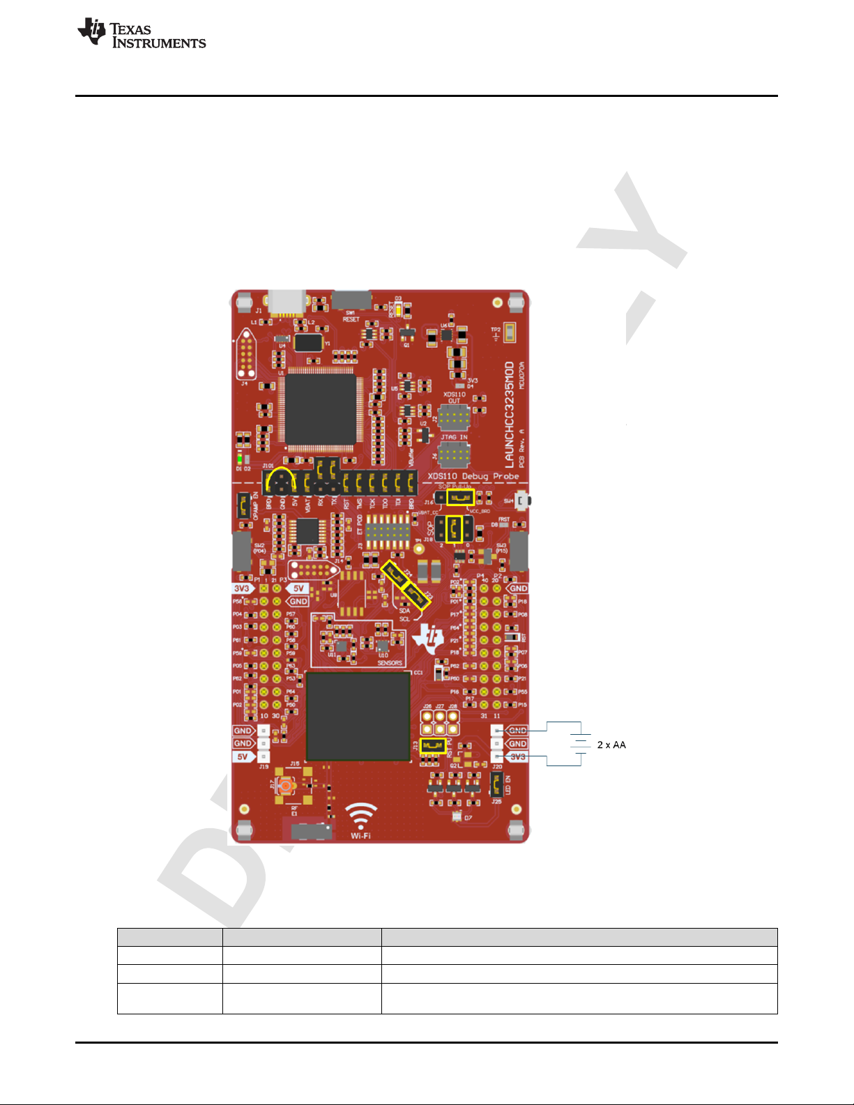
Figure 2 shows the CC3235MODSF LaunchPad EVM.
www.ti.com
Figure 2. CC3235MODSF LaunchPad™ EVM Overview
10
CC3235MODSF LaunchPad™ Development Kit (LAUNCHCC3235MOD)
Copyright © 2019, Texas Instruments Incorporated
SWRU548A–February 2019
Submit Documentation Feedback
Page 11
TI Confidential – NDA Restrictions
CC3235
MAC/PHY
WRF_BGN F
BGN
RF_ANT1
32-Mbit
SFlash
External SPI
Programming
40 MHz
32.768 kHz
UART
SPI
nReset
PM
2.3 V to 3.6 V
VBAT
User GPIOx
Aband
F
D
5 GHz
SPDT
WRF_A
www.ti.com
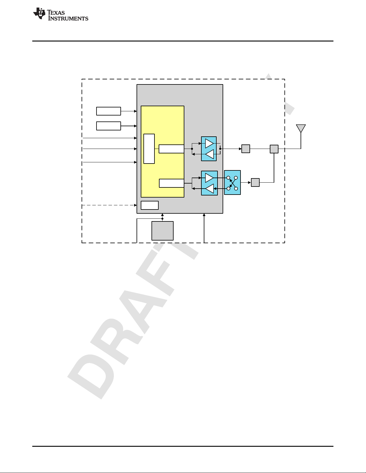
2.1 Block Diagram
Figure 3 shows a functional block diagram of the CC3235MODx module.
Hardware
Figure 3. CC3235MODx Functional Block Diagram
SWRU548A–February 2019
Submit Documentation Feedback
Copyright © 2019, Texas Instruments Incorporated
CC3235MODSF LaunchPad™ Development Kit (LAUNCHCC3235MOD)
11
Page 12
TI Confidential – NDA Restrictions
CC3235MODSF12MOBR
Acc
BMA280
Temperature
Sensor
TMP116
Two 20-pin LaunchPad headers
(compatible with TI MCU standard)
INT (GPIO13)
I2C
FTDI
FT2232D
and
SWD Circuit
USB
Connector
LDO
3.3 V
VCC
Two AA
Battery
Connectors
Reverse
Protection
Push buttons
GPIO13, GPIO22
RGB LED
GPIO9, GPIO10, GPIO11
JTAG and SWD
UART (Flashing)
Hardware
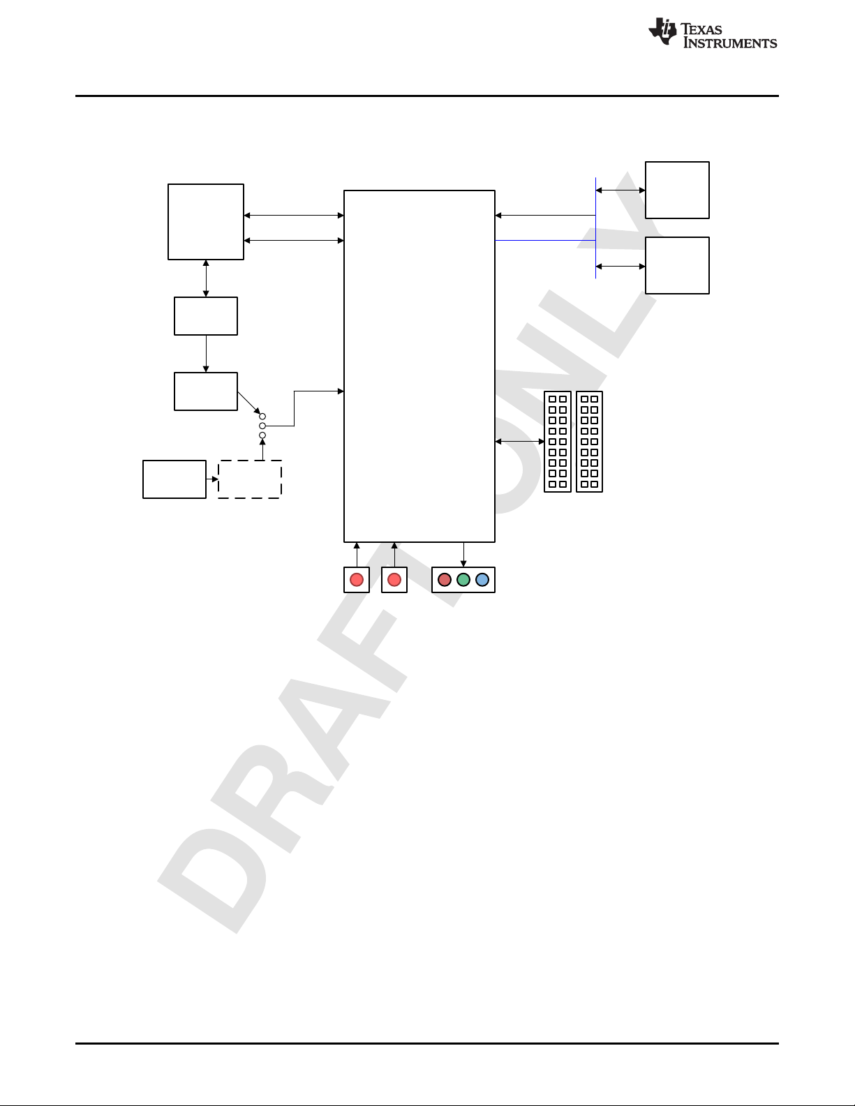
Figure 4 shows a functional block diagram of the LAUNCHCC3235MOD SimpleLink LaunchPad.
www.ti.com
Figure 4. LAUNCHCC3235MOD Functional Block Diagram
12
CC3235MODSF LaunchPad™ Development Kit (LAUNCHCC3235MOD)
Copyright © 2019, Texas Instruments Incorporated
SWRU548A–February 2019
Submit Documentation Feedback
Page 13

TI Confidential – NDA Restrictions
www.ti.com
2.2 Hardware Features
• CC3235MODSF, SimpleLinkTMDual-Band Wi-Fi®module solution with integrated MCU
• 40-pin LaunchPad™ standard that leverages the BoosterPack™ ecosystem
• TI Standard XDS110-based JTAG emulation with serial port for flash programming
• Supports both 4-wire JTAG and 2-wire SWD
• Two buttons and a RGB LED for user interaction
• Virtual COM port UART through USB on PC
• Onboard chip antenna with U.FL or SMA for conducted testing, selectable using 0-Ω resistors
• Onboard accelerometer and temperature sensor for out-of-box demo, with the option to isolate them
from the inter-integrated circuit (I2C) bus
• Micro USB connector for power and debug connections
• Headers for current measurement and external JTAG connection, with an option to use the onboard
XDS110 to debug customer platforms
• Bus-powered device, with no external power required for Wi-Fi
• Long-range transmission with a highly optimized antenna (200-meter typical in open air with a 6-dBi
antenna AP)
• Can be powered externally, working down to 2.3 V
2.2.1 Key Benefits
The CC3235MODx modules offer the following benefits:
• Fully Integrated and Green/RoHS Modules Includes All Required Clocks, SPI Flash, and Passives
• 802.11 a/b/g/n: 2.4 GHz and 5 GHz
• FCC, IC/ISED, ETSI/CE, and MIC Certified
• FIPS 140-2 Level 1 Validated IC Inside
• Multilayered security features, help developers protect identities, data, and software IP
• Low-Power Modes for battery powered application
• Coexistence with 2.4 GHz Radios
• Industrial Temperature: –40°C to +85°C
• CC3235MODx Multiple-core architecture, system-on-chip (SoC)
• 1.27-mm Pitch QFM Package for Easy Assembly and Low-Cost PCB Design
• Transferrable Wi-Fi Alliance®Certification
• Application microcontroller subsystem:
– Arm®Cortex®-M4 core at 80 MHz
– User-dedicated memory
• 256 KB RAM
• Optional 1 MB executable Flash
– Rich set of peripherals and timers
– 26 I/O pins with flexible multiplexing options
• UART, I2S, I2C, SPI, SD, ADC, and 8-bit parallel interface
• 8-bit Synchronous Image Interface
• Timers and PWM
– Debug Interfaces: JTAG, cJTAG, and SWD
Hardware
®
SWRU548A–February 2019
Submit Documentation Feedback
CC3235MODSF LaunchPad™ Development Kit (LAUNCHCC3235MOD)
Copyright © 2019, Texas Instruments Incorporated
13
Page 14

TI Confidential – NDA Restrictions
Hardware
• Wi-Fi network processor subsystem:
• Multilayered security features:
• Application Throughput
www.ti.com
– Wi-Fi®core:
• 802.11 a/b/g/n 2.4 GHz and 5 GHz
• Modes:
• Access Point (AP)
• Station (STA)
• Wi-Fi Direct®(only supported on 2.4 GHz)
• Security:
• WEP
• WPA™/WPA2™ PSK
• WPA2 Enterprise
– Internet and application protocols:
• HTTPs server, mDNS, DNS-SD, DHCP
• IPv4 and IPv6 TCP/IP stack
• 16 BSD sockets (fully secured TLS v1.2 and SSL 3.0)
– Built-in power management subsystem:
• Configurable low-power profiles (always, intermittent, tag)
• Advanced low-power modes
• Integrated DC/DC regulators
– Separate execution environments
– Networking security
– Device identity and key
– Hardware accelerator cryptographic engines (AES, DES, SHA/MD5, CRC)
– Application-level security (encryption, authentication, access control)
– Initial secure programming
– Software tamper detection
– Secure boot
– Certificate signing request (CSR)
– Unique per device key pair
– UDP: 16 Mbps
– TCP: 13 Mbps
14
CC3235MODSF LaunchPad™ Development Kit (LAUNCHCC3235MOD)
Copyright © 2019, Texas Instruments Incorporated
SWRU548A–February 2019
Submit Documentation Feedback
Page 15

TI Confidential – NDA Restrictions
www.ti.com
• Power-Management Subsystem:
• Additional Integrated Components
• Footprint Compatible QFM Package
• Module Supports SimpleLink Developer's Ecosystem
Hardware
– Integrated DC/DC converters support a wide range of supply voltage:
• VBAT wide-voltage mode: 2.3 V to 3.6 V
• VIO is always tied with VBAT
– Advanced low-power modes:
• Shutdown: 1 µA, hibernate: 5.5 µA
• Low-power deep sleep (LPDS): 120 µA
• Idle connected (MCU in LPDS): 710 µA
• RX traffic (MCU active): 59 mA
• TX traffic (MCU active): 223 mA
– Wi-Fi TX Power
• 2.4 GHz: 16.5 dBm at 1 DSSS
• 5 GHz: 15.1 dBm at 6 OFDM
– Wi-Fi RX Sensitivity
• 2.4 GHz: –94.5 dBm at 1 DSSS
• 5 GHz: –89 dBm at 6 OFDM
– 40.0 MHz Crystal
– 32.768 kHz Crystal (RTC)
– 32 Mbit SPI Serial Flash
– RF Filters, Diplexer and Passive Components
– CC3235MODx: 1.27-mm Pitch,
63-Pin, 20.5-mm × 17.5-mm
SWRU548A–February 2019
Submit Documentation Feedback
CC3235MODSF LaunchPad™ Development Kit (LAUNCHCC3235MOD)
Copyright © 2019, Texas Instruments Incorporated
15
Page 16
TI Confidential – NDA Restrictions
Hardware
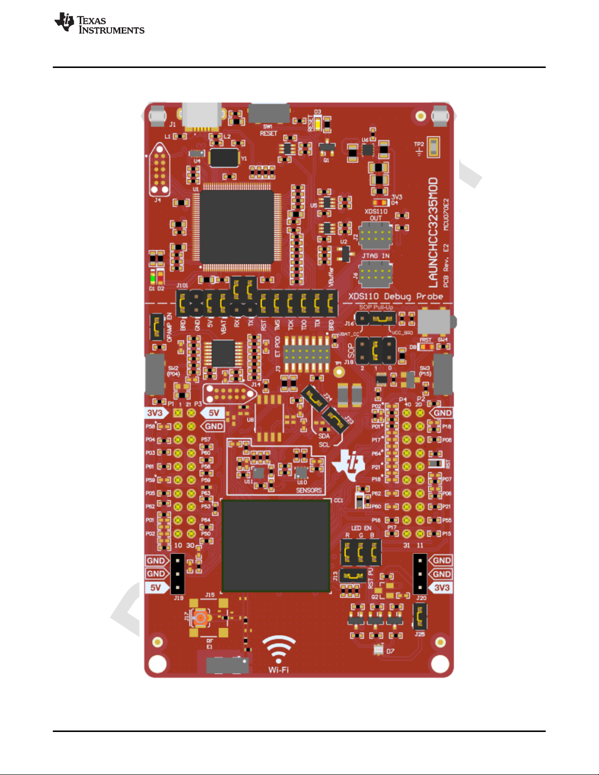
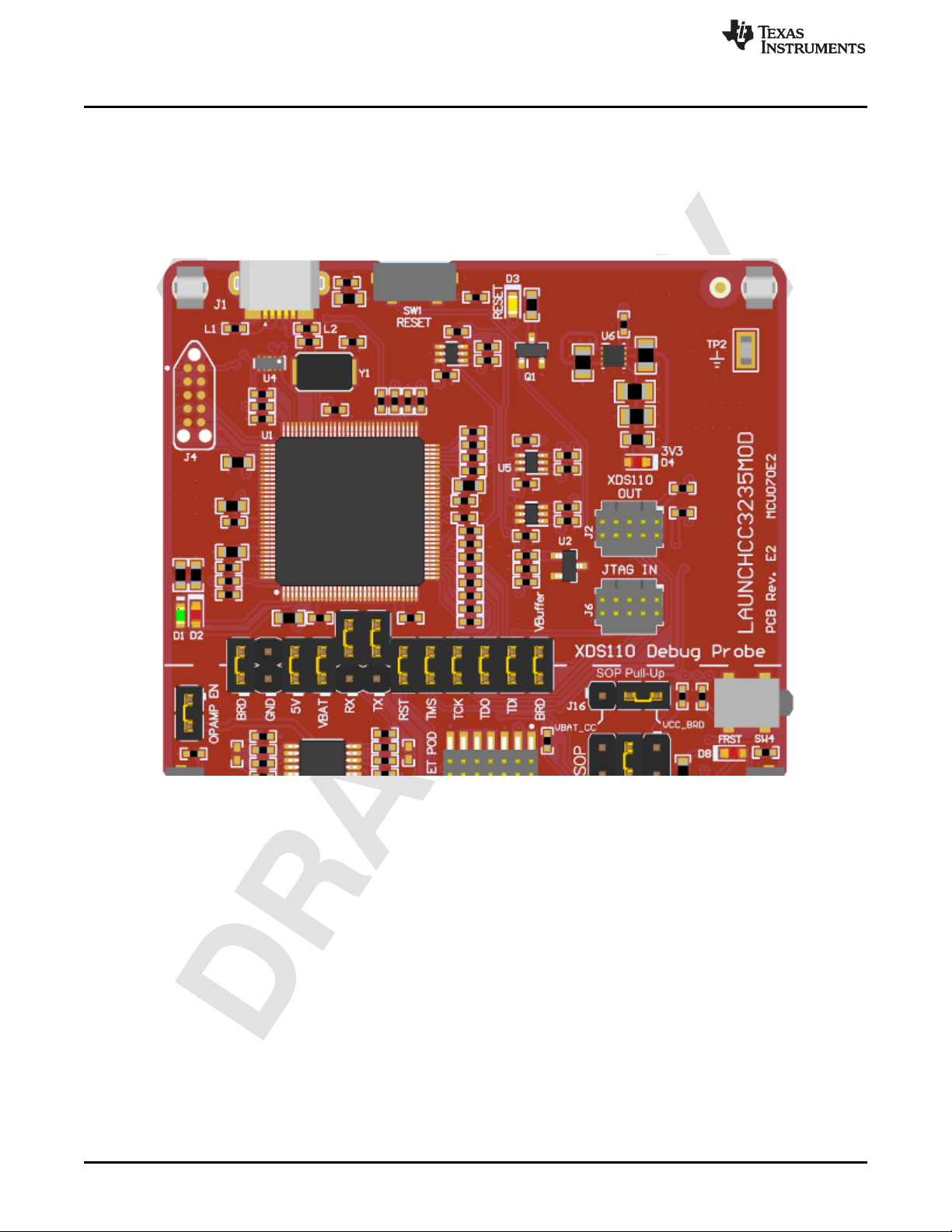
2.2.2 XDS110-Based Onboard Debug Probe
To keep development easy and cost effective, TI's LaunchPad development kits integrate an onboard
debug probe, which eliminates the need for expensive programmers. The CC3235MODSF LaunchPad
has the XDS-110-based debug probe (see Figure 5), which is a simple and low-cost debugger that
supports nearly all TI Arm device derivatives.
Figure 5. XDS-110 Debug Probe
www.ti.com
16
The dotted line through J101 shown in Figure 5 divides the XDS110 debug probe from the target area.
The signals that cross this line can be disconnected by jumpers on J101, the isolation jumper block. More
details on the isolation jumper block are in Section 2.2.3.
The XDS110 debug probe also provides a "backchannel" UART-over-USB connection with the host, which
can be very useful during debugging and for easy communication with a PC. More details can be found in
Section 2.2.4.
The XDS110 debug probe hardware can be found in the schematics in Section 7.2 and in the
CC3235MOD LaunchPad hardware design files.
CC3235MODSF LaunchPad™ Development Kit (LAUNCHCC3235MOD)
Copyright © 2019, Texas Instruments Incorporated
SWRU548A–February 2019
Submit Documentation Feedback
Page 17

TI Confidential – NDA Restrictions
www.ti.com
2.2.3 Debug Probe Connection: Isolation Jumper Block
The isolation jumper block at jumper J101 allows the user to connect or disconnect signals that cross from
the XDS110 domain into the CC3235MOD target domain. This includes JTAG signals, application UART
signals, and 3.3-V and 5-V power.
Reasons to open these connections:
• To remove any and all influence from the XDS110 debug probe for high accuracy target power
measurements
• To control 3-V and 5-V power flow between the XDS110 and target domains
• To expose the target MCU pins for other use than onboard debugging and application UART
communication
• To expose the programming and UART interface of the XDS110 so that it can be used for devices
other than the onboard MCU.
Table 1. Isolation Block Connections
Jumper Description
BRD Board Power. Supplies the board power from the onboard DC-DC converter. The board power
includes the sensors, LED, and the OPAMP used to drive the ADC input.
GND Ground reference
5V 5-V VBUS from USB
VBAT 3.3-V rail, derived from VBUS in the XDS110 domain. Can also be used to measure the current
flowing into the CC3235MOD.
RX Backchannel UART: The target CC3235MODSF receives data through this signal.
TX Backchannel UART: The target CC3235MODSF sends data through this signal.
RST This pin functions as the RST signal (active low).
TMS Serial wire data input (SWDIO) / JTAG test mode select (TMS)
TCK Serial wire clock input (SWCLK) / JTAG clock input (TCK)
TDO JTAG test data out
TDI JTAG test data in
VBUFFER Used to power the level shifters located on the emulator side of the board. The level shifters can
be powered by shorting this pin with a jumper. Removing the jumper enables low current
measurement.
Hardware
SWRU548A–February 2019
Submit Documentation Feedback
CC3235MODSF LaunchPad™ Development Kit (LAUNCHCC3235MOD)
Copyright © 2019, Texas Instruments Incorporated
17
Page 18

TI Confidential – NDA Restrictions
Hardware
2.2.4 Application (or "Backchannel") UART
The board supports a USB-based virtual COM port, using the Tiva™ Arm®MCU. The LaunchPad is
shipped with the UART lines from the CC3235MODSF connected to the UART on the Tiva MCU. The
CC3235MODSF's UART can also be routed to the 20-pin connector for use as a GPIO or external UART.
The selection is performed using jumpers on the board.
Figure 6 shows the UART routed to USB COM port. Ensure that a jumper is also placed on the VBUFFER
header to power the level shifters located on the emulator side of the board. Figure 7 shows the UART
routed to 20-pin header connector.
Figure 6. UART Routed to USB COM Port
www.ti.com
Figure 7. UART Routed to 20-Pin Header Connector
18
CC3235MODSF LaunchPad™ Development Kit (LAUNCHCC3235MOD)
Copyright © 2019, Texas Instruments Incorporated
SWRU548A–February 2019
Submit Documentation Feedback
Page 19

TI Confidential – NDA Restrictions
www.ti.com
2.2.5 JTAG Headers
The headers are provided on the board to isolate the CC3235MOD from the onboard XDS110-based
JTAG emulator. These jumpers are shorted by default when the board is shipped from TI. Figure 5 and
Table 1 are for default configurations, and Figure 8 shows the external emulator connection. To connect
an external emulator, remove the isolation block JTAG jumpers and place the external emulator on the
JTAG IN connector.
Hardware
Figure 8. JTAG IN Connector (J6)
SWRU548A–February 2019
Submit Documentation Feedback
CC3235MODSF LaunchPad™ Development Kit (LAUNCHCC3235MOD)
Copyright © 2019, Texas Instruments Incorporated
19
Page 20

TI Confidential – NDA Restrictions
Hardware
2.2.6 Using the XDS110 Debug Probe with a Different Target
The XDS110 debug probe on the LaunchPad development kit can interface to most Arm®Cortex®-M
devices, not just the onboard target CC3235MODSF device. This functionality is enabled by the J2 10-pin
Cortex-M JTAG connector (see Figure 9) and a 10-pin cable, such as the FFSD-05-D-06.00-01-N (sold
separately from the LaunchPad development kit).
Figure 9. XDS110 OUT Connector (J2)
www.ti.com
20
Header J2 follows the Arm®Cortex®-M standard; however, pin 1 is not a voltage sense pin. The XDS110
outputs only 3.3-V JTAG signals. If another voltage level is needed, the user must provide level shifters to
translate the JTAG signal voltages.
1. Remove jumpers on the JTAG signals on the isolation block, including RST, TMS, TCK, TDO, and TDI.
2. Plug the 10-pin cable into J2, and connect to an external target.
a. J2 follows the Arm®Cortex®Debug Connector standard outlined in Cortex-M Debug Connectors.
3. Plug USB power into the LaunchPad development kit, or power it externally
a. JTAG levels are 3.3-V ONLY
CC3235MODSF LaunchPad™ Development Kit (LAUNCHCC3235MOD)
Copyright © 2019, Texas Instruments Incorporated
SWRU548A–February 2019
Submit Documentation Feedback
Page 21

TI Confidential – NDA Restrictions
www.ti.com
2.2.7 Power Connections
The board accommodates various power methods, including through the onboard XDS110 as well as
external or BoosterPack plug-in module power (see Figure 10).
Figure 10. LAUNCHCC3235MOD Power Block Diagram
Hardware
SWRU548A–February 2019
Submit Documentation Feedback
CC3235MODSF LaunchPad™ Development Kit (LAUNCHCC3235MOD)
Copyright © 2019, Texas Instruments Incorporated
21
Page 22

TI Confidential – NDA Restrictions
Hardware
2.2.7.1 XDS110 USB Power
The most common power-supply scenario is from USB through the XDS110 debugger. This provides 5-V
power from the USB and also regulates this power rail to 3.3 V for XDS110 operation and 3.3-V to the
target side of the LaunchPad development kit. Power from the XDS110 is controlled by jumper J101.
When the board is powered from the USB connector, ensure that the jumpers are placed on the following
headers, shown in Figure 11.
Figure 11. Powering the CC3235MODSF LP from USB
www.ti.com
22
CC3235MODSF LaunchPad™ Development Kit (LAUNCHCC3235MOD)
Copyright © 2019, Texas Instruments Incorporated
SWRU548A–February 2019
Submit Documentation Feedback
Page 23
TI Confidential – NDA Restrictions
www.ti.com
2.2.7.2 BoosterPack Plug-in Module and External Power Supply
Headers J19 and J20 are present on the board to supply external power directly when USB power is not
available. Use the following precautions before using the board with an external power supply.
1. Remove the USB cable.
2. Ensure that jumpers are only placed on the headers shown in Figure 12.
3. Use a jumper wire to connect VBAT and BRD.
4. Plug in the external power supply on J20 with the correct polarity.
Figure 12. Powering the CC3235MODSF LP from an External Power Supply
Hardware
The OPAMP EN and LED EN jumpers are also available to remove any current draw from the onboard
OpAmp and LEDs being driven by the GPIOs, see Table 2.
Reference Use Comments
J19 5-V power input Used to power the board from an external 5-V supply
J20 3.3-V power input Used to power the board from an external 3.3-V supply.
J21 OPAMP EN If uninstalled, the power supply to the operational amplifier is cut off. This can
SWRU548A–February 2019
Submit Documentation Feedback
Table 2. External Supply Connections and Enable Jumpers
be used to enable low-power measurements.
CC3235MODSF LaunchPad™ Development Kit (LAUNCHCC3235MOD)
Copyright © 2019, Texas Instruments Incorporated
23
Page 24

TI Confidential – NDA Restrictions
Hardware
Table 2. External Supply Connections and Enable Jumpers (continued)
Reference Use Comments
J26 LED EN If uninstalled, the LEDs connected to the GPIO are disabled; this can be used
2.2.8 Reset Pullup Jumper
Table 3 lists the reset pullup jumper.
Reference Use Comments
J13 RESET pullup Install this jumper to enable the pullup resistor on the nRESET pin of the
2.2.9 Clocking
All of the required clocks are inside the module. There is no need to supply any external clock.
www.ti.com
to enable low-power measurements.
Table 3. Reset Pullup Jumper
device, when the board is powered from an external supply.
24
CC3235MODSF LaunchPad™ Development Kit (LAUNCHCC3235MOD)
Copyright © 2019, Texas Instruments Incorporated
SWRU548A–February 2019
Submit Documentation Feedback
Page 25
TI Confidential – NDA Restrictions
www.ti.com
2.2.10 I2C Connection
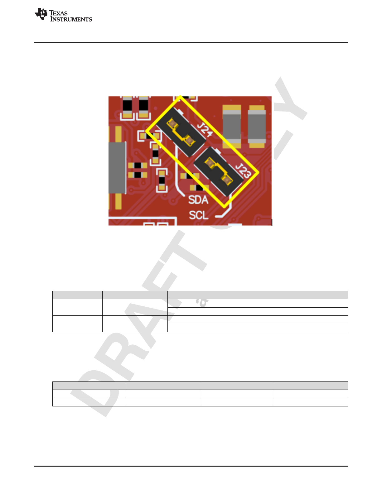
The board features an accelerometer and a temperature sensor for the out-of-box demo. These are
connected to the I2C bus, and can be isolated using the jumpers provided (shown as yellow jumpers J23
and J24 in Figure 13).
Hardware
Figure 13. I2C Connections
By removing J23 and J24, the accelerometer and the temperature sensors are isolated from the I2C bus.
This measure also removes the I2C pullup resistors from the sensor side of the circuit, and therefore any
connection to the circuit requires the user to install external pullup resistors.
Table 4 lists the I2C jumper definitions.
Reference Use Comments
J23 I2C SCL Populated: CC3235MOD SCL connected to onboard sensors with pullup
J24 I2C SDA Populated: CC3235MOD SDA connected to onboard sensors with pullup
2.2.10.1 Default I2C Addresses
Table 5 lists the default I2C addresses of the onboard sensors.
Table 5. Default I2C Addresses (of Onboard Sensors)
Sensor Type Reference Designator on LP Part Number (Manufacturer) Default Slave Address (Hex)
Temperature (Digital ) U10 TMP116 (TI) 0x49
Accelerometer (Triaxial) U11 BMA280 (Bosch) 0x30
Table 4. I2C Jumper Definitions
Open: CC3235MOD SCL disconnected from onboard sensors
Open: CC3235MOD SDA disconnected from onboard sensors
SWRU548A–February 2019
Submit Documentation Feedback
CC3235MODSF LaunchPad™ Development Kit (LAUNCHCC3235MOD)
Copyright © 2019, Texas Instruments Incorporated
25
Page 26
TI Confidential – NDA Restrictions
Hardware
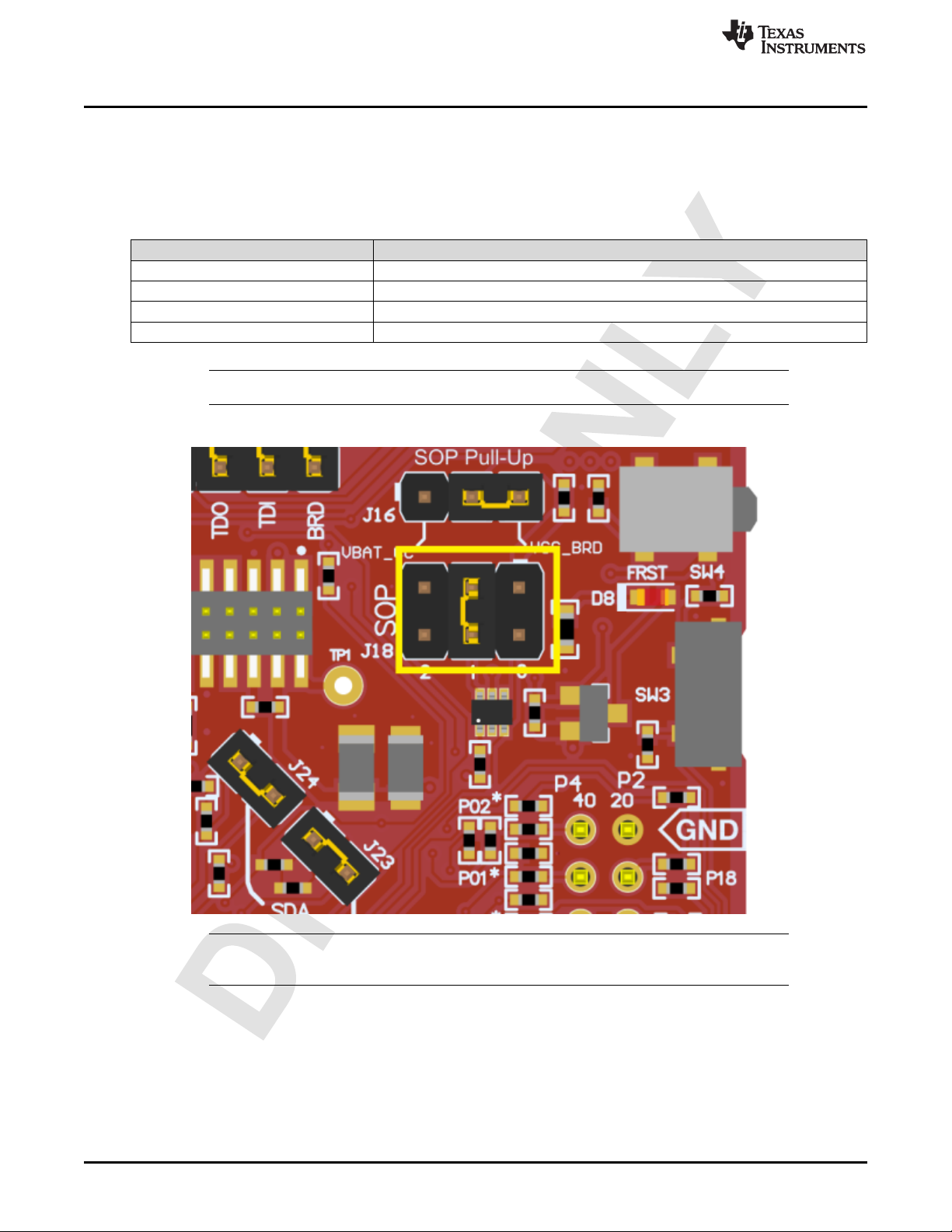
2.2.11 Sense on Power (SOP)
The CC3235MODx device can be set to operate in four different modes based on the state of the sense
on power (SOP) lines. The SOP lines are pins 23, 24, and 34 on the CC3235MODx module. Table 6
shows the state of the device and Figure 14 shows the SOP jumpers.
Binary Value Function
100 Flash programming
000 Functional mode + 4-wire JTAG
001 Functional mode + SWD
010 Functional mode + flash
NOTE: SOP[2:0] corresponds to J18 on the LaunchPad design.
Figure 14. SOP Jumpers (Default Setting Shown)
www.ti.com
Table 6. SOP[2:0]
26
NOTE: Placing no jumpers on the block ensures that the line is pulled low using 100K pull down
resistors. Placing the jumper pulls the pin high using a 10K resistor.
CC3235MODSF LaunchPad™ Development Kit (LAUNCHCC3235MOD)
Copyright © 2019, Texas Instruments Incorporated
Submit Documentation Feedback
SWRU548A–February 2019
Page 27

TI Confidential – NDA Restrictions
www.ti.com
2.2.12 Push-Buttons and LED Indicators
Table 7 lists the push-button definitions.
Table 7. Push-Button Definitions
Reference Use Comments
SW1 RESET This is used to reset the CC3235MOD device. This signal is also output on the
SW2 GPIO_13 When pushed, GPIO_13 is pulled to VCC.
SW3 GPIO_22 When pushed, GPIO_22 is pulled to VCC.
SW4 Factory default Pressing this button and toggling RESET restores the factory default image on
Table 8 lists the LED indicators.
Reference Color Use Comments
D1,D2 Green and Red Debug Indicates the state of the JTAG
D3 Yellow nRESET Indicates the state of the NRESET
D4 Red Power Indicates when the 3.3-V power is
D7 RGB GPIO_09 Glows when the GPIO is logic-1.
RGB GPIO_10
RGB GPIO_11
D8 Red Factory Reset Indicates that the push-button for
(1)
GPIO_10 and GPIO_11 are also used as I2C. Whenever the pullups are enabled, the LEDs glow by default without configuring
the GPIOs.
Hardware
20-pin connector to reset any external BoosterPack which may be stacked. The
reset can be isolated using the RST jumper at the isolation block.
the serial flash. This can be used to recover a corrupted serial flash, provided
the s-flash was programmed with a recovery image.
Table 8. LED Indicators
emulator. For TI use only.
pin. If this LED is on, the device is
functional.
supplied to the board.
(1)
(1)
Glows when the GPIO is logic-1.
Glows when the GPIO is logic-1.
the factory reset is pressed.
2.3 Electrical Characteristics
For electrical characteristics of the CC3235MODx modules, see CC3235MODx SimpleLink™ Wi-Fi
CERTIFIED®Dual-Band Wireless MCU Module data sheet.
2.4 Antenna Characteristics
The CC3235MODSM2MOB and the CC3235MODSF12MOB reference design detail the use of an onboard antenna. For more information on the antenna VSWR, efficiency, and electrical characteristics, see
M830520.
SWRU548A–February 2019
Submit Documentation Feedback
CC3235MODSF LaunchPad™ Development Kit (LAUNCHCC3235MOD)
Copyright © 2019, Texas Instruments Incorporated
27
Page 28
TI Confidential – NDA Restrictions
Hardware
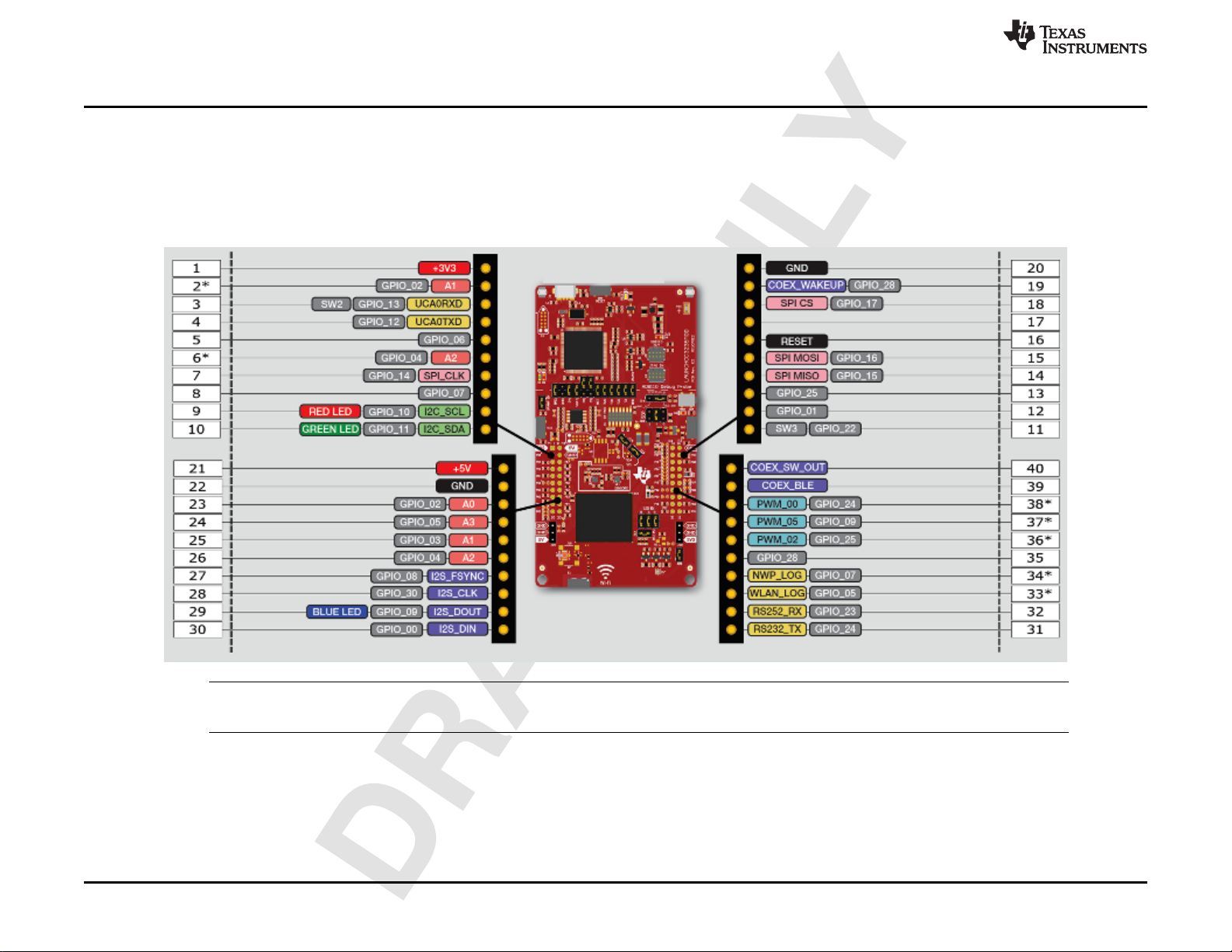
2.5 BoosterPack™ Header Pin Assignment
The BoosterPack header pinout specification is at Build Your Own BoosterPack. Also see the BoosterPack Pinout Standard.
The CC3235MODSF LaunchPad follows this standard, with the exception of naming. (P1:P4 is used instead of J1:J4.). See Figure 15 for the
CC3235MODSF LaunchPad pin-mapping assignments and functions.
Figure 15. LAUNCHCC3235MOD BoosterPack™ Header Pin Assignments
www.ti.com
NOTE: RESET output is an open-drain-type output and can only drive the pin low. The pullup ensures that the line is pulled back high when the
button is released. No external BoosterPack can drive this pin low.
All the signals are referred to by the pin number in the SDK; Figure 15 shows the default mappings. Some of the pins are repeated across the
connector. For instance, pin 62 is available on P1 and P4, but only P1 is connected by default. The signal on P4 is marked with an asterisk (*) to
signify that it is not connected by default. The signal can be routed to the pin by using a 0-Ω resistor in the path. For the exact resistor placement,
see the CC3235MODSF SimpleLinkTMWi-Fi®Wireless MCU LaunchPad Board Design Files.
28
CC3235MODSF LaunchPad™ Development Kit (LAUNCHCC3235MOD)
SWRU548A–February 2019
Submit Documentation Feedback
Copyright © 2019, Texas Instruments Incorporated
Page 29
TI Confidential – NDA Restrictions
www.ti.com
3 Layout Guidelines
The integrator of the CC3235MODx modules must comply with the PCB layout recommendations
described in the following subsections to preserve and minimize the risk with regulatory certifications for
FCC, ISED/IC, ETSI/CE, and MIC. Also, TI recommends that customers follow the guidelines described in
this section to achieve similar performance.
3.1 LAUNCHCC3235MOD Board Layout
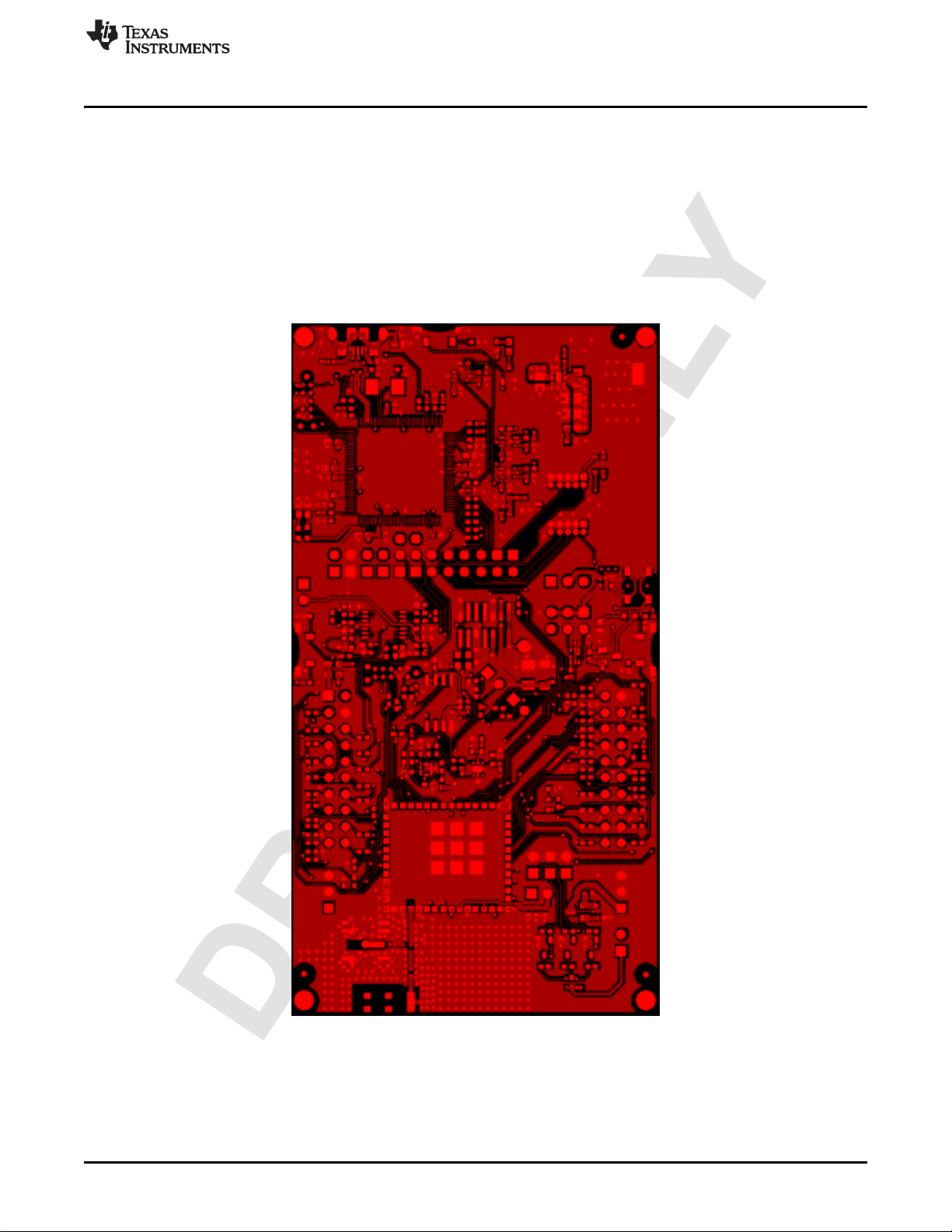
The reference layout consists of a four-layer design. Figure 16 shows the LAUNCHCC3235MOD top layer.
Figure 16. LAUNCHCC3235MOD Top Layer
Layout Guidelines
SWRU548A–February 2019
Submit Documentation Feedback
CC3235MODSF LaunchPad™ Development Kit (LAUNCHCC3235MOD)
Copyright © 2019, Texas Instruments Incorporated
29
Page 30
TI Confidential – NDA Restrictions
Layout Guidelines
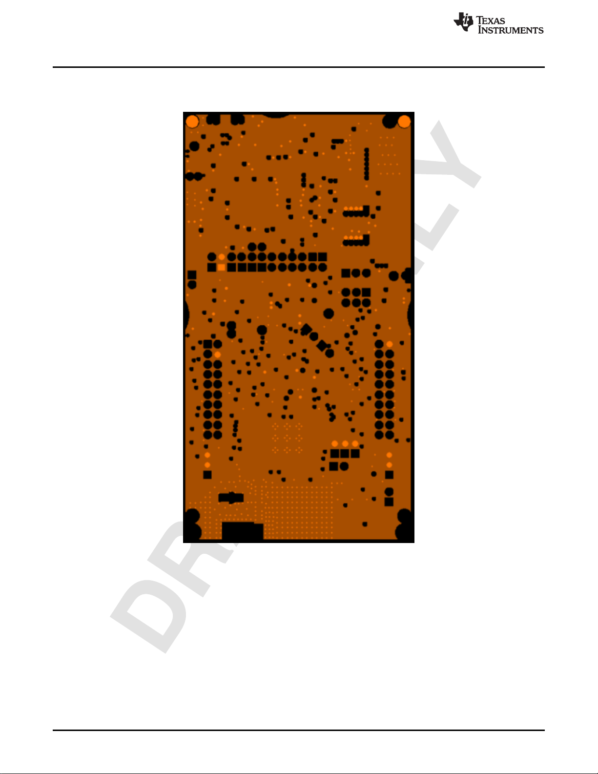
Figure 17 shows the LAUNCHCC3235MOD first inner layer.
www.ti.com
Figure 17. LAUNCHCC3235MOD First Inner Layer
30
CC3235MODSF LaunchPad™ Development Kit (LAUNCHCC3235MOD)
Copyright © 2019, Texas Instruments Incorporated
SWRU548A–February 2019
Submit Documentation Feedback
Page 31
TI Confidential – NDA Restrictions
www.ti.com
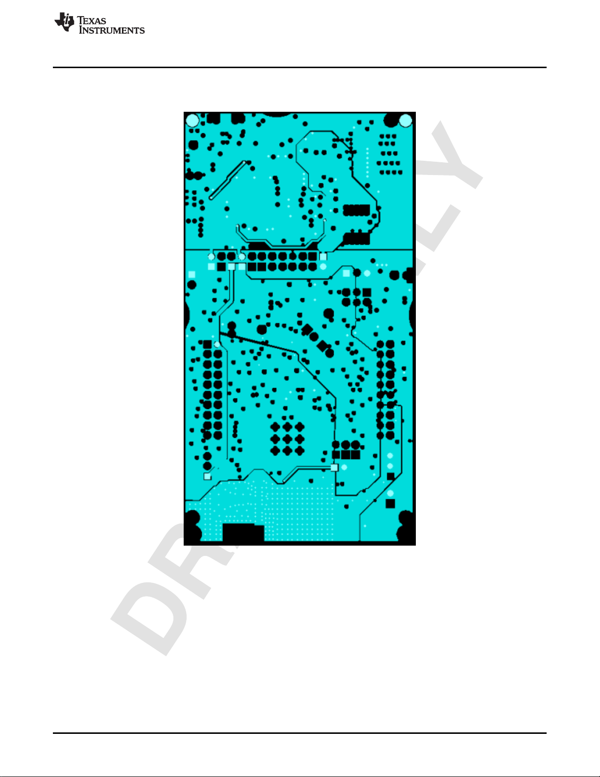
Figure 18 shows the LAUNCHCC3235MOD second inner layer.
Layout Guidelines
Figure 18. LAUNCHCC3235MOD Second Inner Layer
SWRU548A–February 2019
Submit Documentation Feedback
CC3235MODSF LaunchPad™ Development Kit (LAUNCHCC3235MOD)
Copyright © 2019, Texas Instruments Incorporated
31
Page 32

TI Confidential – NDA Restrictions
Layout Guidelines
Figure 19 shows the LAUNCHCC3235MOD bottom layer.
www.ti.com
Figure 19. LAUNCHCC3235MOD Bottom Layer
32
CC3235MODSF LaunchPad™ Development Kit (LAUNCHCC3235MOD)
Copyright © 2019, Texas Instruments Incorporated
SWRU548A–February 2019
Submit Documentation Feedback
Page 33

TI Confidential – NDA Restrictions
www.ti.com
3.2 General Layout Recommendations
Ensure that the following general layout recommendations are followed:
• Have a solid ground plane and ground vias under the module for stable system and thermal
dissipation.
• Do not run signal traces underneath the module on a layer where the module is mounted.
3.3 RF Layout Recommendations
The RF section of this wireless module gets top priority in terms of layout. It is very important for the RF
section to be laid out correctly to ensure optimum performance from the module. A poor layout can cause
low-output power, EVM degradation, sensitivity degradation, and mask violations.
Figure 20 shows the RF placement and routing of the CC3235MODSF module.
Figure 20. RF Section Layout
Layout Guidelines
SWRU548A–February 2019
Submit Documentation Feedback
CC3235MODSF LaunchPad™ Development Kit (LAUNCHCC3235MOD)
Copyright © 2019, Texas Instruments Incorporated
33
Page 34

TI Confidential – NDA Restrictions
Copyright © 2017, Texas Instruments Incorporated
Layout Guidelines
Use the following RF layout recommendations for the CC3235MODx module:
• RF traces must have 50-Ω impedance.
• RF trace bends must be made with gradual curves, and 90 degree bends must be avoided.
• RF traces must not have sharp corners.
• There must be no traces or ground under the antenna section.
• RF traces must have via stitching on the ground plane beside the RF trace on both sides.
• RF traces must be as short as possible. The antenna, RF traces, and the module must be on the edge
of the PCB product in consideration of the product enclosure material and proximity.
For optimal RF performance, ensure the copper cut out on the top layer under the RF-BG pin (pin 31) is
as shown in Figure 21.
www.ti.com
Figure 21. Top Layer Copper Pullback on RF Pads
34
CC3235MODSF LaunchPad™ Development Kit (LAUNCHCC3235MOD)
Copyright © 2019, Texas Instruments Incorporated
SWRU548A–February 2019
Submit Documentation Feedback
Page 35

TI Confidential – NDA Restrictions
www.ti.com
3.4 Antenna Placement and Routing
The antenna is the element used to convert the guided waves on the PCB traces to the free space
electromagnetic radiation. The placement and layout of the antenna are the keys to increased range and
data rates. Table 9 provides a summary of the recommended antennas to use with the CC3235MODx
module.
SR NO. GUIDELINES
1 Place the antenna on an edge or corner of the PCB.
2 Ensure that no signals are routed across the antenna elements on all the layers of the PCB.
3
4
5 Ensure that the antenna impedance is 50 Ω because the module is rated to work only with a 50-Ω system.
6 In case of printed antenna, ensure that the simulation is performed with the solder mask in consideration.
7 Ensure that the antenna has a near omnidirectional pattern.
8
Most antennas, including the chip antenna used on the LaunchPad, require ground clearance on all the layers of
the PCB. Ensure that the ground is cleared on inner layers as well.
Ensure that there is provision to place matching components for the antenna. These must be tuned for best
return loss when the complete board is assembled. Any plastics or casing must also be mounted while tuning
the antenna because this can impact the impedance.
The feed point of the antenna is required to be grounded. This is only for the antenna type used on the
CC3235MODx LaunchPad. See the specific antenna data sheets for the recommendations.
Layout Guidelines
Table 9. Antenna Guidelines
3.5 Transmission Line Considerations
The RF signal from the module is routed to the antenna using a Coplanar Waveguide with ground (CPWG) structure. CPW-G structure offers the maximum amount of isolation and the best possible shielding to
the RF lines. In addition to the ground on the L1 layer, placing GND vias along the line also provides
additional shielding. Figure 22 shows a cross section of the coplanar waveguide with the critical
dimensions.
Figure 22. Coplanar Waveguide (Cross Section)
SWRU548A–February 2019
Submit Documentation Feedback
CC3235MODSF LaunchPad™ Development Kit (LAUNCHCC3235MOD)
Copyright © 2019, Texas Instruments Incorporated
35
Page 36

TI Confidential – NDA Restrictions
S
W
Layout Guidelines
Figure 23 shows the top view of the coplanar waveguide with GND and via stitching.
The recommended values for the PCB are provided for 2-layer boards in Table 10 and for 4-layer boards
in Table 11.
www.ti.com
Figure 23. CPW With GND and Via Stitching (Top View)
Table 10. Recommended PCB Values for 2-Layer Board
(L1 to L2 = 42.1 mils)
PARAMETER VALUE UNIT
W 26 mils
S 5.5 mils
H 42.1 mils
Er (FR-4 substrate) 4.2 F/m
Table 11. Recommended PCB Values for 4-Layer Board
(L1 to L2 = 16 mils)
PARAMETER VALUE UNITS
W 21 mils
S 10 mils
H 16 mils
Er (FR-4 substrate) 4.5 F/m
36
CC3235MODSF LaunchPad™ Development Kit (LAUNCHCC3235MOD)
Copyright © 2019, Texas Instruments Incorporated
SWRU548A–February 2019
Submit Documentation Feedback
Page 37

TI Confidential – NDA Restrictions
www.ti.com
4 Operational Setup and Testing
A compatible BoosterPack can be stacked on top of the LaunchPad using the two, 20-pin connectors. The
connectors do not have a key to prevent the misalignment of the pins or reverse connection. Ensure that
the VCC and 5-V pins are aligned with the BoosterPack header pins. On the CC3235MODSF LaunchPad,
a small white symbol is provided near pin 1 (see Figure 24) to orient all BoosterPacks.
Figure 24. Pin 1 Marking on LaunchPad (3V3 Mark)
Operational Setup and Testing
SWRU548A–February 2019
Submit Documentation Feedback
CC3235MODSF LaunchPad™ Development Kit (LAUNCHCC3235MOD)
Copyright © 2019, Texas Instruments Incorporated
37
Page 38

TI Confidential – NDA Restrictions
Operational Setup and Testing
4.1 Measuring the CC3235MOD Current Draw
To measure the current draw of the CC3235MOD device using a multimeter, use the VBAT jumper on the
J101 isolation block. The current draw measured in this mode includes only the CC3235MOD device,
Serial Flash, any current drawn through the BoosterPack plug-in module headers. However, if a GPIO of
the CC3235MOD is driving a high current load like the LED, then that is also included in this
measurement.
4.1.1 Low-Current Measurement with USB Power (<1 mA)
See the following instructions to measure ultra-low power when powering with a USB cable (see ).
1. Remove the VBAT jumper in the J101 isolation block, and attach an ammeter across this jumper.
2. Consider the effect that the backchannel UART and any circuitry attached to the CC3235MOD may
have on current draw. Consider disconnecting these at the siolation jumper block, or at least consider
their current sinking and sourcing capability in the final measurement.
3. Begin target execution and set the device to low-power modes (LPDS or hibernate).
4. Measure the current. Remember that if the current levels are fluctuating, it may be difficult to get a
stable measurement. It is easier to measure quiescent states.
4.1.2 Active Current Measurements
See the following instructions to measure active power.
1. Remove the VBAT jumper (J18).
2. Solder a 0.1-Ω resistor on a wire which can be connected to a voltmeter/oscilloscope. Or, attach a
jumper across J18 so that it can be used with a current probe.
3. Measure the voltage across the resistor using an oscilloscope with a differential probe. For the current
probe, coil the wire around the sensor several times for good sensitivity.
• An ammeter can also be used for this measurement, but the results may be erroneous due to the
switching nature of the current
www.ti.com
38
CC3235MODSF LaunchPad™ Development Kit (LAUNCHCC3235MOD)
Copyright © 2019, Texas Instruments Incorporated
SWRU548A–February 2019
Submit Documentation Feedback
Page 39

TI Confidential – NDA Restrictions
www.ti.com
4.2 RF Connections
4.2.1 AP Connection Testing
By default, the board ships with the 2.4 GHz and 5 GHz RF signals routed to the onboard chip antenna,
as shown in Figure 25.
Figure 25. Using Onboard Antenna (Default Condition)
Operational Setup and Testing
A U.FL connector J17 provides a way to test in the lab using a compatible cable. Alternatively, trackpads
for an SMA connector J15 are provided onboard to replace the J17 U.FL connector for testing conducted
measurements. A rework must be performed before these connectors can be used; this involves swapping
the position of a resistor. Figure 26 shows the modified board.
Figure 26. Board Modified for External Antenna Connections (Measure 2.4 GHz or 5 GHz)
SWRU548A–February 2019
Submit Documentation Feedback
CC3235MODSF LaunchPad™ Development Kit (LAUNCHCC3235MOD)
Copyright © 2019, Texas Instruments Incorporated
39
Page 40

TI Confidential – NDA Restrictions
Operational Setup and Testing
4.3 Design Files
4.3.1 Hardware Design Files
Schematics can be found in Section 7.2.All design files, including schematics, layout, Bill of Materials
(BOM), Gerber files, and documentation are available for download from LAUNCHCC3235MOD.
4.4 Software
All design files, including firmware patches, software example projects, and documentation are available
from the CC3235 Software Development Kit. Inside of the SDK, a set of very simple CC3235 code
examples can be found that demonstrates how to use the entire set of CC3235 peripherals. When starting
a new project or adding a new peripheral, these examples serve as a great starting point.
5 Development Environment Requirements
The following software examples with the LaunchPad require an integrated development environment
(IDE) that supports the CC3235MOD.
The CC313x and CC323x SimpleLink™ Wi-Fi®Embedded Programming User's Guide has detailed
information about software environment setup with examples. See this document for further details on the
software sample examples.
5.1 CCS
CCS 6.0 or higher is required. When CCS is launched, and a workspace directory is chosen, use
Project → Import Existing CCS Eclipse Project. Direct it to the desired demo project directory containing
main.c.
www.ti.com
5.2 IAR
IAR 6.70 or higher is required. To open the demo in IAR, choose File → Open → Workspace…, and direct
it to the *.eww workspace file inside the \IAR subdirectory of the desired demo. All workspace information
is within this file.
The subdirectory also has an *.ewp project file; this file can be opened into an existing workspace, using
Project → Add-Existing-Project….
40
CC3235MODSF LaunchPad™ Development Kit (LAUNCHCC3235MOD)
Copyright © 2019, Texas Instruments Incorporated
SWRU548A–February 2019
Submit Documentation Feedback
Page 41

TI Confidential – NDA Restrictions
www.ti.com
6 Additional Resources
6.1 CC3235MODx Product Page
For more information on the CC3235MOD device, visit the CC3235MOD product page, which includes the
CC3235MODx SimpleLink™ Wi-Fi®Wireless and Internet-of-Things Solution, a Single-Chip Wireless MCU
data sheet and key documents such as the CC32xx SimpleLink™ Wi-Fi® and Internet-of-Things Technical
Reference Manual.
6.2 Download CCS, IAR
Although the files can be viewed with any text editor, more can be done with the projects if they are
opened with a development environment such as Code Composer Studio (CCS), IAR, or Energia. CCS
and IAR are each available in a full version, or a free, code-size-limited version. The full out-of-box demo
cannot be built with the free version of CCS or IAR (IAR Kickstart), due to the code-size limit. To bypass
this limitation, a code-size-limited CCS version is provided that has most functionality integrated into a
library. The code built into the library is able to be viewed by the user, but it cannot be edited. For full
functionality, download the full version of either CCS or IAR.
6.3 SimpleLink™ Academy for CC3235 SDK
The SimpleLink™ Academy is a collection of curated training modules developed by TI subject matter
experts to help developers get up and running as quickly as possible with a SimpleLink MCU device and
its SDK. The training is delivered using TI Resource Explorer, which offers a powerful cloud-enabled
environment that includes background information, interactive exercises, code snippets, quizzes, and
more.
Experience the SimpleLink™ Academy now using the TI Resource Explorer at dev.ti.com.
Additional Resources
Figure 27. CC32xx SimpleLink™ Academy
6.4 TI E2E Community
Search the forums at e2e.ti.com. If you cannot find your answer, post your question to the community!
SWRU548A–February 2019
Submit Documentation Feedback
CC3235MODSF LaunchPad™ Development Kit (LAUNCHCC3235MOD)
Copyright © 2019, Texas Instruments Incorporated
41
Page 42
TI Confidential – NDA Restrictions
Assembly Drawing and Schematics
7 Assembly Drawing and Schematics
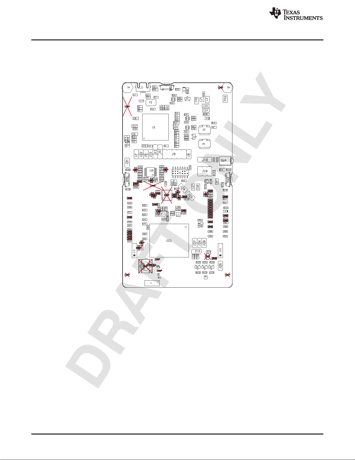
7.1 Assembly Drawing
Figure 28. LAUNCHCC3235MOD Top-Layer Assembly Drawing
www.ti.com
42
CC3235MODSF LaunchPad™ Development Kit (LAUNCHCC3235MOD)
Copyright © 2019, Texas Instruments Incorporated
SWRU548A–February 2019
Submit Documentation Feedback
Page 43

TI Confidential – NDA Restrictions
PD0/AIN15/C0O/I2C7SCL/SSI2XDAT1/T0CCP0
1
PD1/AIN14/C1O/I2C7SDA/SSI2XDAT0/T0CCP1
2
PD2/AIN13/C2O/I2C8SCL/SSI2FSS/T1CCP0
3
PD3/AIN12/I2C8SDA/SSI2CLK/T1CCP1
4
PE3/AIN0/U1DTR
12
PE2/AIN1/U1DCD
13
PE1/AIN2/U1DSR
14
PE0/AIN3/U1RTS
15
PC7/C0-/EPI0S4/U5TX
22
PC6/C0+/EPI0S5/U5RX
23
PC5/C1+/EPI0S6/RTCCLK/U7TX
24
PC4/C1-/EPI0S7/U7RX
25
PH0/EPI0S0/U0RTS
29
PH1/EPI0S1/U0CTS
30
PH2/EPI0S2/U0DCD
31
PH3/EPI0S3/U0DSR
32
PA0/CAN0RX/I2C9SCL/T0CCP0/U0RX
33
PA1/CAN0TX/I2C9SDA/T0CCP1/U0TX
34
PA2/I2C8SCL/SSI0CLK/T1CCP0/U4RX
35
PA3/I2C8SDA/SSI0FSS/T1CCP1/U4TX
36
PA4/I2C7SCL/SSI0XDAT0/T2CCP0/U3RX
37
PA5/I2C7SDA/SSI0XDAT1/T2CCP1/U3TX
38
PA6/EPI0S8/I2C6SCL/SSI0XDAT2/T3CCP0/U2RX/USB0EPEN
40
PA7/EPI0S9/I2C6SDA/SSI0XDAT3/T3CCP1/U2TX/USB0EPEN/USB0PFLT
41
PF0/EN0LED0/M0PWM0/SSI3XDAT1/TRD2
42
PF1/EN0LED2/M0PWM1/SSI3XDAT0/TRD1
43
PF2/M0PWM2/SSI3FSS/TRD0
44
PF3/M0PWM3/SSI3CLK/TRCLK
45
PF4/EN0LED1/M0FAULT0/SSI3XDAT2/TRD3
46
PG0/EN0PPS/EPI0S11/I2C1SCL/M0PWM4
49
PG1/EPI0S10/I2C1SDA/M0PWM5
50
PB2/EPI0S27/I2C0SCL/T5CCP0/USB0STP
91
PB3/EPI0S28/I2C0SDA/T5CCP1/USB0CLK
92
PB0/CAN1RX/I2C5SCL/T4CCP0/U1RX/USB0ID
95
PB1/CAN1TX/I2C5SDA/T4CCP1/U1TX/USB0VBUS
96
PC3/SWO/TDO
97
PC2/TDI
98
PC1/SWDIO/TMS
99
PC0/SWCLK/TCK
100
PB5/AIN11/I2C5SDA/SSI1CLK/U0RTS
120
PB4/AIN10/I2C5SCL/SSI1FSS/U0CTS
121
PE4/AIN9/SSI1XDAT0/U1RI
123
PE5/AIN8/SSI1XDAT1
124
PD4/AIN7/SSI1XDAT2/T3CCP0/U2RX
125
PD5/AIN6/SSI1XDAT3/T3CCP1/U2TX
126
PD6/AIN5/SSI2XDAT3/T4CCP0/U2RTS/USB0EPEN
127
PD7/AIN4/NMI/SSI2XDAT2/T4CCP1/U2CTS/USB0PFLT
128
PQ0/EPI0S20/SSI3CLK
5
PQ1/EPI0S21/SSI3FSS
6
PQ2/EPI0S22/SSI3XDAT0
11
PK0/AIN16/EPI0S0/U4RX
18
PK1/AIN17/EPI0S1/U4TX
19
PK2/AIN18/EPI0S2/U4RTS
20
PK3/AIN19/EPI0S3/U4CTS
21
PQ3/EPI0S23/SSI3XDAT1
27
PK7/EPI0S24/I2C4SDA/M0FAULT2/RTCCLK/U0RI
60
PK6/EN0LED1/EPI0S25/I2C4SCL/M0FAULT1
61
PK5/EN0LED2/EPI0S31/I2C3SDA/M0PWM7
62
PK4/EN0LED0/EPI0S32/I2C3SCL/M0PWM6
63
PM7/T5CCP1/TMPR0/U0RI
71
PM6/T5CCP0/TMPR1/U0DSR
72
PM5/T4CCP1/TMPR2/U0DCD
73
PM4/T4CCP0/TMPR3/U0CTS
74
PM3/EPI0S12/T3CCP1
75
PM2/EPI0S13/T3CCP0
76
PM1/EPI0S14/T2CCP1
77
PM0/EPI0S15/T2CCP0
78
PL0/EPI0S16/I2C2SDA/M0FAULT3/USB0D0
81
PL1/EPI0S17/I2C2SCL/PHA0/USB0D1
82
PL2/C0O/EPI0S18/PHB0/USB0D2
83
PL3/C1O/EPI0S19/IDX0/USB0D3
84
PL4/EPI0S26/T0CCP0/USB0D4
85
PL5/EPI0S33/T0CCP1/USB0D5
86
PL7/T1CCP1/USB0DM
93
PL6/T1CCP0/USB0DP
94
PQ4/DIVSCLK/U1RX
102
PP2/EPI0S29/U0DTR/USB0NXT
103
PP3/EPI0S30/RTCCLK/U0DCD/U1CTS/USB0DIR
104
PP4/U0DSR/U3RTS/USB0D7
105
PP5/I2C2SCL/U3CTS/USB0D6
106
PN0/U1RTS
107
PN1/U1CTS
108
PN2/EPI0S29/U1DCD/U2RTS
109
PN3/EPI0S30/U1DSR/U2CTS
110
PN4/EPI0S34/I2C2SDA/U1DTR/U3RTS
111
PN5/EPI0S35/I2C2SCL/U1RI/U3CTS
112
PJ0/EN0PPS/U3RX
116
PJ1/U3TX
117
PP0/C2+/SSI3XDAT2/U6RX
118
PP1/C2-/SSI3XDAT3/U6TX
119
TM4C1294NCPDTI3R
U1A
VDD
7
VDDA8GNDA
10
VDD
16
GND
17
VDD
26
VDD
28
VDD
39
VDD
47
GND
48
VDD
51
VDD
52
GND
55
GND
58
VBAT
68
VDD
69
VDD
79
GND
80
VDDC
87
VDD
90
VDD
101
VDD
113
GND
114
VDDC
115
VDD
122
TM4C1294NCPDTI3R
U1C
33.0R2
33.0R4
33.0R6
33.0R7
33.0R8
33.0R9
33.0R10
XDS_UART_RX
XDS_UART_TX
XDS_JTAG_TCK
XDS_JTAG_TMS
XDS_JTAG_TDO
XDS_JTAG_TDI
ITCK
ITMS
ITDI
ITDO
330k
R11
VBUS_USB1
220k
R12
0.01uF
C2
GND
Red
D2
220
R15
LED0
Green
D1
LED1
220
R14
GND
1.0kR16
1.0kR17
1.0kR18
1.0kR20
VCC_LDO_3V3
GND
XDSET_P
XDSET_N
51R23
VCC_LDO_3V3
1uF
C3
GND
GND
0.01uFC50.01uFC60.01uFC70.1uFC80.1uFC90.1uF
C10
GND
0.01uF
C14
1uF
C15
GND
2.2uF
C16
0.1uF
C17
1uF
C18
GND
VCC_LDO_3V3
TM4C HOST MCU FOR EMULATION
XDSET_P
XDSET_N
0R3
XDSET_ID
100R5 VBUS_USB1
0.1uF
C1
GND
ID -> PK[7:4] =0x07
XDS_JTAG_TCK
XDS_JTAG_TMS
XDS_JTAG_TDO
XDS_JTAG_TDI
XDS_nRESET
XDSET_ID
VCC_LDO_3V3
1.0k
R1
VCC_BRD
1 2
3 4
5 6
7 8
9 10
J6
1.0k
R13
VCC_LDO_3V3
1 2
3 4
5 6
7 8
9 10
J2
P55_GPIO_01
P57_GPIO_02
1.0k
R19
33
R22
33
R21
P01_GPIO_10
P02_GPIO_11
TP1
1 2
3 4
5 6
7 8
9 10
11 12
13 14
J3
VBAT_CC
VBAT_CC
GND
GND GND
GND
WAKE
64
HIB
65
XOSC0
66
XOSC1
67
RST
70
OSC0
88
OSC1
89
EN0RXIN
53
EN0RXIP
54
EN0TXON
56
EN0TXOP
57
VREFA+
9
RBIAS
59
TM4C1294NCPDTI3R
U1B
10k
R24
VCC_LDO_3V3
100
R25
IRSTN
GND
VREFA
4.87k
R27
GND
1
2
16MHz
Y1
22pF
C11
22pF
C4
GND
VCC_LDO_3V3
1.0k
R26
123
LM4040B25IDBZR
U2
0.01uF
C12
1uF
C13
GND
VREFA
VCC_LDO_3V3
GND
ITMS
ITCK
ITDO
ITDI
IRSTN
1
2
3
4
5 6
7
8
9
10
J4
CMP-0075101-1
DNP
XDS_JTAG_TMS
XDS_JTAG_TCK
XDS_JTAG_TDO
XDS_JTAG_TDI
XDS_CC_nRESET
P20_JTAG_TMS
P19_JTAG_TCK
P17_JTAG_TDO
P16_JTAG_TDI
CC_nRESET
www.ti.com
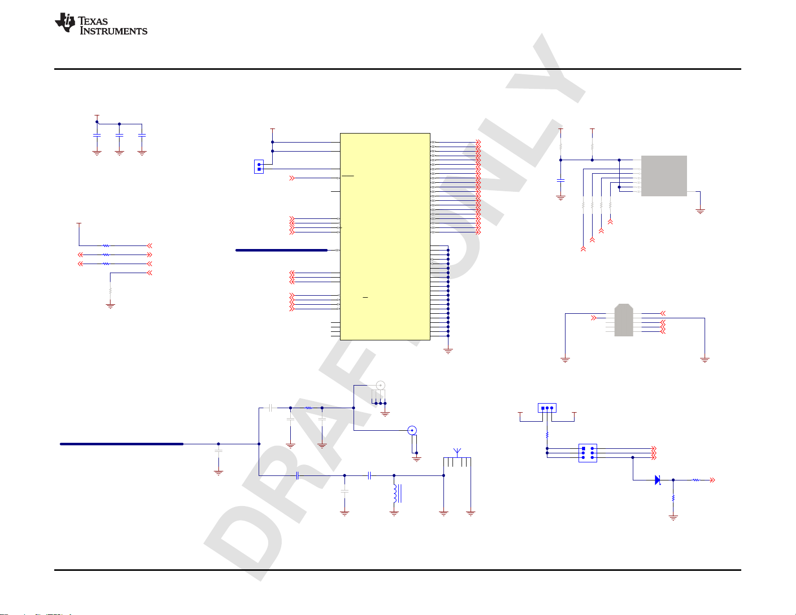
7.2 Schematics
Assembly Drawing and Schematics
Figure 29. Schematics (1 of 5)
SWRU548A–February 2019
Submit Documentation Feedback
Copyright © 2019, Texas Instruments Incorporated
CC3235MODSF LaunchPad™ Development Kit (LAUNCHCC3235MOD)
43
Page 44

TI Confidential – NDA Restrictions
100k
R31
0.01uF
C21
GND
10 ohm
L1
10 ohm
L2
VBUS_USB1
GND
D1+
1
D1-
2
GND
3
D2+
4
D2-
5
NC
6
NC
7
GND
8
NC
9
NC
10
TPD4S010DQAR
U4
GND
USB-INTERFACE
XDSET_N
XDSET_P
XDSET_ID
VCC_Buffer VCC_LDO_3V3
A
3
VCCA
1
B
4
DIR
5
GND
2
VCCB
6
SN74LVC1T45DCKR
U3
0.1uF
C20
XDS_nRESET
GND
GNDGND
0.1uF
C19
100k
R28
GND
12
34
56
78
910
J5
61301021121
10k R29
XDS_JTAG_TDI
XDS_JTAG_TDO
XDS_JTAG_TCK
XDS_JTAG_TMS
P19_JTAG_TCK
P20_JTAG_TMS
CC_nRESET
P17_JTAG_TDO
P16_JTAG_TDI
GND
VCC_Buffer
Yellow
D3
XDS_UART_RX
P55_GPIO_01
LP_GPIO_01
VCC_Buffer VCC_LDO_3V3
33.0
R34
A
3
VCCA
1
B
4
DIR
5
GND
2
VCCB
6
SN74LVC1T45DCKR
U5
0.1uF
C22
0.1uF
C23
100k
R33
123
J11
XDS_UART_TX
P57_GPIO_02
LP_GPIO_02
VCC_Buffer VCC_LDO_3V3
0.1uF
C29
0.1uF
C30
A
3
VCCA
1
B
4
DIR
5
GND
2
VCCB
6
SN74LVC1T45DCKR
U7
GND
GND
GND
GNDGND
GND
GND
GND
1
2
3
J12
33.0
R37
GND
to Host-MCUto Targ et
10uF
C24
100uF
C27
100uF
C28
10uF
C26
270
R35
J9
J10
J7 J8
2.2uH
L3
22uF
C25
100k
R36
CHECK LAYOUT GUIDE FROM DATASHEET
POWER MANAGEMENT
TPS62162DSGR
PGND
1
VIN
2
EN
3
AGND
4
FB
5
VOS
6
SW
7
PG
8
EP
9
U6
VBUS_USB1 VCC_MCU_5V
VCC_LDO_3V3 VCC_BRD VCC_Buffer
VBAT_CC
GND
GND GND GND GNDGND GND
VOLTA GE TRANSLATORS
Red
D4
XDS_CC_nRESET
1
2
3
Q1
BSS138
100
R32
VBUS
1
D-
2
D+
3
ID
4
GND
5
678
11109
J1
1
2
3
4
SW1
390
R30
Assembly Drawing and Schematics
www.ti.com
Figure 30. Schematics (2 of 5)
CC3235MODSF LaunchPad™ Development Kit (LAUNCHCC3235MOD)
44
Copyright © 2019, Texas Instruments Incorporated
SWRU548A–February 2019
Submit Documentation Feedback
Page 45
TI Confidential – NDA Restrictions
P50_GPIO_00
P55_GPIO_01
P57_GPIO_02
P58_GPIO_03
P59_GPIO_04
P60_GPIO_05
P61_GPIO_06
P62_GPIO_07
P63_GPIO_08
P64_GPIO_09
P01_GPIO_10
P02_GPIO_11
P03_GPIO_12
P04_GPIO_13
P07_GPIO_16
P08_GPIO_17
P15_GPIO_22
P18_GPIO_28
P53_GPIO_30
P05_GPIO_14
P06_GPIO_15
RF_ABG
P20_JTAG_TMS
P19_JTAG_TCK
P17_JTAG_TDO
P16_JTAG_TDI
J13
VBAT_CC
CC_nRESET
100k
R47
DNP
GND
0R45
0R46
P17_GPIO_24
P16_GPIO_23
0.1uF
C31
0.1uF
C32
0.1uF
C33
GND GND GND
VBAT_CC
VBAT_CC
1
2
3
J16
VCC_BRD
1 2
3 4
5 6
J18
SOP1
100kR44
VBAT_CC
CS
1
SO/SIO1
2
WP/SIO2
3
GND
4
SI/SIO0
5
SCLK
6
RESET/SIO3
7
VCC
8
U8
MX25R6435FM2IL0
DNP
GND
0
R39
DNP
0
R38
DNP
0
R40
DNP
0
R41
DNP
0
R42
DNP
0
R43
DNP
VCC_BRD VBAT_CC
0.1uF
C34
GND
1
2
3
4
5 6
7
8
9
10
J14
TC2050-IDC-NL-FP
DNP
GND
GND
GND
D5
P21_GPIO_25
10k
R52
GND
2.2k
R51
OUTPUT ONLY
10k
R49
CC3235MOD TA RGET EXTERNAL FLASH
GANG PROGRAMMING CONNECTOR
SOP JUMPERS
SOP0
GND
1
2
345
6
E1
M830520
Feed
GND GND GND
GND
1
2
345
J15
DNP
GND
GNDGND
RF SECTION
RF_ABG
0.5pF
C40
DNP
GND
1
2
3
J17
SPI_MISO
SPI_CS_IN
SPI_CLK
SPI_MOSI
SPI_CS_IN
P17_JTAG_TDO
P16_JTAG_TDI
P19_JTAG_TCK
SOP2
SOP0
SOP1
SOP2
SPI_MISO
SPI_MOSI
SPI_CLK
SPI_CS_IN
SPI_CS_IN
SPI_CLK
SPI_MISO
SPI_MOSI
CC_nRESET
0.5pF
C36
DNP
0.5pF
C37
DNP
0.5pF
C38
DNP
GND
1
GND
2
GPIO10
3
GPIO11
4
GPIO14
5
GPIO15
6
GPIO16
7
GPIO17
8
GPIO12
9
GPIO13
10
GPIO22
11
JTAG_TDI
12
FLASH_SPI_MISO
13
FLASH_SPI_CS_IN
14
FLASH_SPI_CLK
15
GND
16
FLASH_SPI_MOSI
17
JTAG_TDO
18
GPIO28
19
NC
20
JTAG_TCK
21
JTAG_TMS
22
SOP2
23
SOP1
24
GND
25
GND
26
GND
27
GND
28
GND
29
GND
30
RF_ABG
31
GND
32
NC
33
SOP0
34
RESET
35
VBAT_RESET
36
VBAT1
37
GND
38
NC
39
VBAT2
40
NC
41
GPIO30
42
GND
43
GPIO0
44
NC
45
GPIO01
46
GPIO02
47
GPIO03
48
GPIO04
49
GPIO05
50
GPIO06
51
GPIO07
52
GPIO08
53
GPIO09
54
GND
55
GND
56
GND
57
GND
58
GND
59
GND
60
GND
61
GND
62
GND
63
CC3235MODSF12MOBR
CC1
1pF
C39
4.7nH
L4
0
C35
8.2pF
R50
8.2pF
R48
DNP
www.ti.com
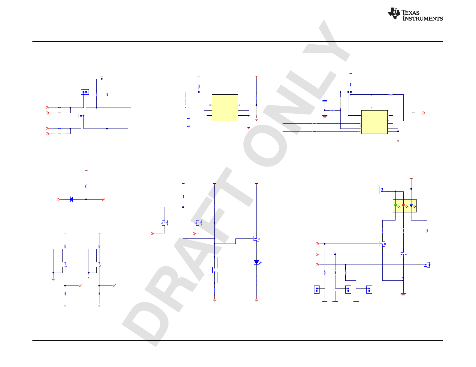
Assembly Drawing and Schematics
Figure 31. Schematics (3 of 5)
SWRU548A–February 2019
Submit Documentation Feedback
CC3235MODSF LaunchPad™ Development Kit (LAUNCHCC3235MOD)
Copyright © 2019, Texas Instruments Incorporated
45
Page 46
TI Confidential – NDA Restrictions
P17_GPIO_24
P02_GPIO_11
P01_GPIO_10
P16_GPIO_23
SENS_I2C_SCL
SENS_I2C_SDA
I2C BUS SELECTION
0R130
0R134
DNP
0R137
0R139
DNP
J23
J24
SWITCHES & FACTORY RESET
LP_RESET_OUTCC_nRESET
VCC_BRD
100k
R142
D6
CDBU00340
LED INDICAT ORS
P02_GPIO_11
P01_GPIO_10
P64_GPIO_09
GND GND GND
GND
1
2
3
Q5
BSS138
1
2
3
Q6
BSS138
1
2
3
Q7
BSS138
J26 J27 J28
100k
R150
100k
R151
100k
R152
TEMP SENSOR
VCC_BRD
GND
0
R125
0
R128
0
R132
DNP
0
R136
0
R135
SENS_I2C_SDA
SENS_I2C_SCL
0.1uF
C46
GND
GND
GND
ACCELEROMETER
P04_GPIO_13
SENS_I2C_SDA
SENS_I2C_SCL
VCC_BRD
0.1uF
C48
0.1uF
C47
0
R129
DNP
0
R131
0R138
0R141
0
R133
DNP
0
R124
GND
P04_GPIO_13 P15_GPIO_22
GND
GND
1.0k
R148
1.0k
R149
10k
R155
10k
R156
GND GND
SOP1 SOP0
VCC_BRDVCC_BRD
3.3k
R126
3.3k
R127
VCC_BRD VCC_BRD VCC_BRD
J25
100k
R144
2
1
6
Q3A BSS84DW-7-F
5
4
3
Q3B
413
2
SW4
EVQ-PSD02K
1.0k
R154
3
1
2
Q4
FDN358P
Red
D8
270
R153
VCC_BRD VCC_BRD
VCC_BRD
GND
GND GND
SCL
1
GND
2
ALERT
3
ADD0
4
V+
5
SDA
6
PAD
7
TMP116AIDRVR
U10
SDO
1
SDX
2
VDDIO
3
NC
4
INT1
5
INT2
6
VDD
7
GNDIO
8
GND
9
CSB
10
PS
11
SCX
12
U11
BMA280
0
R140
1
2
3
4
SW2
1
2
3
4
SW3
24
R147
110
R146
16
R145
1
42536
B
R
G
D7
19-337/R6GHBHC-A01/2T
10k
R143
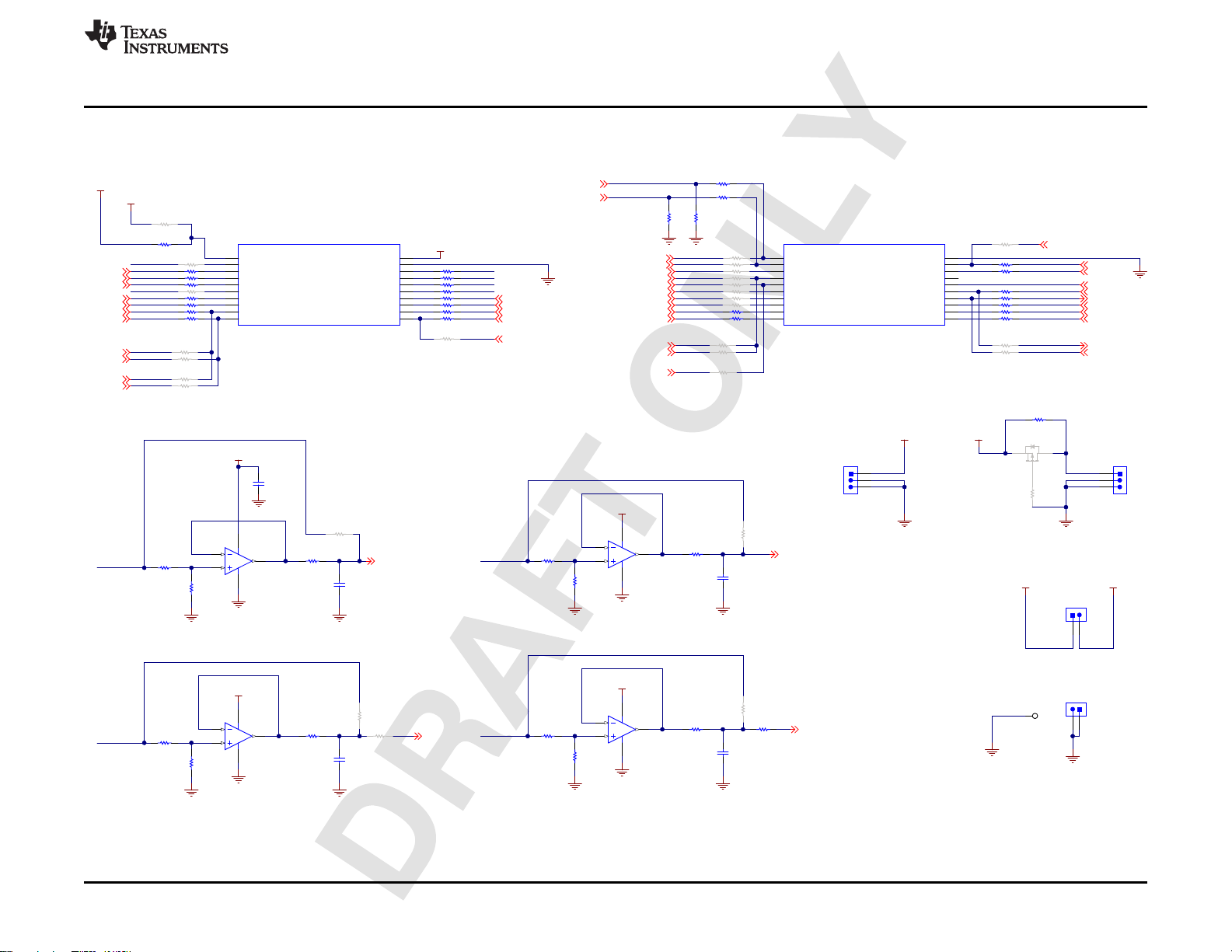
Assembly Drawing and Schematics
www.ti.com
Figure 32. Schematics (4 of 5)
46
CC3235MODSF LaunchPad™ Development Kit (LAUNCHCC3235MOD)
Copyright © 2019, Texas Instruments Incorporated
SWRU548A–February 2019
Submit Documentation Feedback
Page 47
TI Confidential – NDA Restrictions
0
R105
DNP
0
R104
3
1
2
Q2
FDN358P
DNP
TP2
GND GND
GND
VCC_MCU_5V VBAT_CC
+3.3V
1
Analog_In
2
LP_UART_RX
3
LP_UART_TX
4
GPIO !
5
Analog In
6
SPI_CLK
7
GPIO !
8
I2C_SCL
9
I2C_SDA
10
+5V
21
GND
22
Analog_In
23
Analog_In
24
Analog_In
25
Analog_In
26
Analog_In/I2S_WS
27
Analog_In/I2S_SCLK
28
Analog_Out/I2S_SDout
29
Analog_Out/I2S_SDin
30
P1
VCC_MCU_5V
GND
GPIO !
31
GPIO !
32
GPIO !
33
GPIO !
34
Timer_Cap/GPIO !
35
Timer_Cap/GPIO !
36
PWM/GPIO !
37
PWM/GPIO !
38
PWM/GPIO !
39
PWM/GPIO !
40
GPIO !
11
SPI_CS/GPIO !
12
SPI_CS/GPIO !
13
SPI_MISO
14
SPI_MOSI
15
RST
16
GPIO
17
GPIO !
18
PWM/GPIO !
19
GND
20
P2
GND
0
R57
DNP
0
R58
VBAT_CC
VCC_BRD
0R61
DNP
0R64 0R65
0R68 0R69
0R71 0R72
0R74
DNP
0R75
0R78 0R79
0R82 0R83
0R86 0R87
0R90 0R91
0R97
DNP
0R100
DNP
ANA_IN1
ANA_IN4
ANA_IN2
ANA_IN3
P63_GPIO_08
P53_GPIO_30
P64_GPIO_09
P50_GPIO_00
ANA_IN2
P04_GPIO_13
P03_GPIO_12
P61_GPIO_06
ANA_IN3
P05_GPIO_14
P62_GPIO_07
P01_GPIO_10
P02_GPIO_11
P16_GPIO_23
P17_GPIO_24
AlternateI2C
0R60
DNP
0R62
DNP
0R63
0R66
DNP
0R67
0R70
DNP
0R73
DNP
0R76
DNP
0R77
0R80
DNP
0R81
0R84
DNP
0R85
0R88 0R89
0R92 0R93
0R53
0R54
0R95
DNP
0R98
DNP
0R101
DNP
Alternate RTS
Alternate CTS
For Antenna diversity
0R96
DNP
0R99
DNP
SWAP MOSI/MISO
0R94
DNP
P60_GPIO_05
0R102
DNP
0R103
DNP
P03_GPIO_12
P04_GPIO_13
P58_GPIO_03& P50_GPIO_00
can alsobe used for ANTSEL
COEX_SW_OUT&
CC_COEX_BLE_IN routedto
ANTSEL onDiversity Board
100k
R55
100k
R56
GNDGND
P58_GPIO_03
P50_GPIO_00
P17_GPIO_24
P64_GPIO_09
P21_GPIO_25
P18_GPIO_28
P62_GPIO_07
P60_GPIO_05
P16_GPIO_23
P17_GPIO_24
P02_GPIO_11
P01_GPIO_10
P62_GPIO_07
P50_GPIO_00
P61_GPIO_06
0R59
DNP
P59_GPIO_04
LP_RESET_OUT
P07_GPIO_16
P06_GPIO_15
P21_GPIO_25
P08_GPIO_17
LP_GPIO_01
P18_GPIO_28
P15_GPIO_22
P06_GPIO_15
P07_GPIO_16
P59_GPIO_04/ DIO 12 onCC2640R2LP
(COEX_WAKEUP)
J21
VCC_BRD VCC_OPAMP
ADC DRIVER
ANA_IN1
GND
LP_GPIO_02
0.01uF
C41
VCC_OPAMP
576k
R110
422k
R113
GND
1
2
3
4
11
OPA4342EA/250
U9A
5
6
7
4
11
OPA4342EA/250
U9B
8
9
10
4
11
OPA4342EA/250
U9C
12
13
14
4
11
OPA4342EA/250
U9D
0R106
DNP
470
R111
0.01uF
C43
ANA_IN2
VCC_OPAMP
576k
R119
422k
R123
GND
0
R115
DNP
470
R120
0.01uF
C45
P58_GPIO_03
ANA_IN4
VCC_OPAMP
576k
R108
422k
R112
0
R107
DNP
470
R109
0.01uF
C42
ANA_IN3
VCC_OPAMP
576k
R116
422k
R122
0
R114
DNP
470
R117
0.01uF
C44
P60_GPIO_05
P59_GPIO_04
GND
GND
GND
GND
GND
GND
GND
GND
GND
GND
J22
GND
BOOSTER PACK INTERFACE
0
R121
DNP
0
R118
1
2
3
J19
1
2
3
J20
CC_COEX_SW_OUT
CC_COEX_BLE
CC_COEX_WAKEUP
www.ti.com
Assembly Drawing and Schematics
Figure 33. Schematics (5 of 5)
SWRU548A–February 2019
Submit Documentation Feedback
CC3235MODSF LaunchPad™ Development Kit (LAUNCHCC3235MOD)
Copyright © 2019, Texas Instruments Incorporated
47
Page 48

TI Confidential – NDA Restrictions
Revision History
www.ti.com
Revision History
NOTE: Page numbers for previous revisions may differ from page numbers in the current version.
Changes from Original (February 2019) to A Revision .................................................................................................. Page
• Added last paragraph to Section 1.6.2 ................................................................................................. 8
• Added Section 6.3 ....................................................................................................................... 41
48
Revision History
Copyright © 2019, Texas Instruments Incorporated
SWRU548A–February 2019
Submit Documentation Feedback
Page 49

TI Confidential – NDA Restrictions
User's Guide
SWRU548A–February 2019
Manual Information to the End User
1 The OEM integrator must be aware not to provide information to the end user regarding how to install or
remove this RF module in the user’s manual of the end product which integrates this module. The end
user manual must include all required regulatory information and warnings as shown in this manual.
2 RF Function and Frequency Range
The CC3235MODSM2MOB and CC3235MODSF12MOB devices are designed to operate in the WLAN
2.4-GHz and 5-GHz band. The CC3235MODSM2MOB and CC3235MODSF12MOB devices support
the following channels dependent on the region of operation:
• FCC and IC: Ch 1 to 11 (2142 MHz to 2462 MHz) and 36 to 161 (5180 MHz to 5805 MHz)
• EU: Channels 1 through 13 (2142 MHz to 2472 MHz) and 36 to 136 (5180 MHz to 5680 MHz)
• JP: Channels 1 through 13 (2142 MHz to 2472 MHz) and 36 to 136 (5180 MHz to 5680 MHz)
Note that the CC3235MODx devices do not support determination of its region through any external
mechanism. The region is set by the application SW, or at the time of programming of the device. The
end user is unable to change the region of operation at any time.
NOTE: The maximum RF power transmitted in each WLAN 2.4 GHz band is 19 dBm (EIRP power).
The maximum RF power transmitted in each WLAN 5 GHz band is 18.8 dBm (EIRP power).
3 FCC and IC Certification and Statement
This device is intended for OEM integrators under the following conditions:
• The antenna must be installed so 20 cm of space is maintained between the antenna and the users.
• The transmitter module may not be colocated with any other transmitter of antenna.
• To comply with FCC and IC regulations limiting maximum RF output power and human exposure to RF
radiation, the maximum antenna gain including cable loss in a mobile exposure condition must not
exceed:
– +2.5 dBi in WLAN 2.4 GHz
– +4.5 dBi in WLAN 5 GHz
In the event that these conditions cannot be met (for example, certain laptop configurations or
colocation with another transmitter), then the FCC and IC authorization is no longer considered valid
and the FCC and IC ID cannot be used on the final product. In these circumstances, the OEM
integrator will be responsible for re-evaluating the end product (including the transmitter) and obtaining
a separate FCC and IC authorization.
3.1 FCC
The TI CC3235MODx modules are certified for FCC as a single-modular transmitter. The module is an
FCC-certified radio module that carries a modular grant.
You are cautioned that changes or modifications not expressly approved by the party responsible for
compliance could void the user’s authority to operate the equipment. This device complies with Part 15
of the FCC Rules.
Operation is subject to the following two conditions:
• This device may not cause harmful interference.
SWRU548A–February 2019
Submit Documentation Feedback
Copyright © 2019, Texas Instruments Incorporated
Manual Information to the End User
49
Page 50

TI Confidential – NDA Restrictions
FCC and IC Certification and Statement
• This device must accept any interference received, including interference that may cause undesired
operation of the device.
FCC RF Radiation Exposure Statement:
This equipment complies with FCC radiation exposure limits set forth for an
uncontrolled environment. This equipment should be installed and operated
with a minimum distance of 20 cm between the radiator and your body.
This equipment has been tested and found to comply with the limits for a Class B digital device, pursuant
to Part 15 of the FCC rules. These limits are designed to provide reasonable protection against harmful
interference in a residential installation. this equipment generates, uses, and can radiate radio frequency
energy and, if not installed and used in accordance with the instructions, may cause harmful interference
to radio communications. However, there is no guarantee that interference will not occur in a particular
installation. If this equipment does cause harmful interference to radio or television reception, which can
be determined by turning the equipment off and on, the user is encouraged to try to correct the
interference by one or more of the following measures:
• Reorient or relocate the receiving antenna.
• Increase the separation between the equipment and receiver.
• Connect the equipment into an outlet on a circuit different from the one the receiver is connected to.
• Consult the dealer or an experienced radio or TV technician for help.
The antennas listed in Table 12 of this document were verified in the compliance testing. Use only the
antennas listed in Table 12 . A separate approval is required for all other operating configurations,
including different antenna configurations
www.ti.com
CAUTION
3.2 CAN ICES-3(B) and NMB-3(B) Certification and Statement
The TI CC3235MODx modules are certified for IC as a single-modular transmitter. The TI CC3235MODx
modules meet IC modular approval and labeling requirements. The IC follows the same testing and rules
as the FCC regarding certified modules in authorized equipment.
This device complies with Industry Canada license-exempt RSS standards.
Operation is subject to the following two conditions:
• This device may not cause interference.
• This device must accept any interference, including interference that may cause undesired operation of
the device.
Le présent appareil est conforme aux CNR d'Industrie Canada applicables aux appareils radio exempts de
licence.
L'exploitation est autorisée aux deus conditions suivantes:
• L'appareil ne doit pas produire de brouillage.
• L'utilisateur de l'appareil doit accepter tout brouillage radioélectrique subi, même si le brouillage ests
susceptible d'en compromettre lu fonctionnement.
50
Manual Information to the End User
Copyright © 2019, Texas Instruments Incorporated
SWRU548A–February 2019
Submit Documentation Feedback
Page 51

TI Confidential – NDA Restrictions
www.ti.com
IC RF Radiation Exposure Statement:
This equipment complies with IC radiation exposure limits set forth for an
uncontrolled environment. This equipment should be installed and operated
with a minimum distance of 20 cm between the radiator and your body.
Déclaration d'exposition aux radiations:
Cut équipement est conforme aux limites d'exposition aux rayonnements IC
établies pour un environnement non contrôlé. Cet équipement doit être installé
et utilisé avec un minimum de 20 cm de distance entre la source de
rayonnement et votre corps.
This radio transmitter (451I-CC3235MOD) has been approved by Industry Canada to operated with the
antenna types listed in Table 12 of this document with the maximum permissible gain indicated. Antenna
types not included in this list, having a gain greater than the maximum gain indicated for that type, are
strictly prohibited for use with this device.
The antennas listed in Table 12 of this document were verified in the compliance testing. Use only the
antennas listed in Table 12 . A separate approval is required for all other operating configurations,
including different antenna configurations.
3.3 End Product Labeling
This module is designed to comply with the FCC statement, FCC ID: Z64-CC3220MOD. The host
system using this module must display a visible label indicating the following text:
• Contains FCC ID: Z64-CC3235MOD
This module is designed to comply with the IC statement, IC: 451I-CC3220MOD. The host system
using this module must display a visible label indicating the following text:
• Contains IC: 451I-CC3235MOD
This module is designed to comply with JP statement 201-190033. The host system using this module
must display a visible label indicating the following text:
• Contains transmitter module with certificate module 201-190033
FCC and IC Certification and Statement
CAUTION
3.4 Device Classifications
Because host devices vary widely with design features and configurations, module integrators shall
reference the following guidelines regarding device classification and simultaneous transmission, and
seek guidance from their preferred regulatory test lab to determine how regulatory guidelines will
impact the device compliance. Proactive management of the regulatory process will minimize
unexpected schedule delays and costs due to unplanned testing activities.
The module integrator must determine the minimum distance required between their host device and
the body of the user. The FCC provides device classification definitions to assist in making the correct
determination. Note that these classifications are guidelines only; strict adherence to a device
classification may not satisfy the regulatory requirement as near-body device design details may vary
widely. The user-preferred test lab will be able to assist in determining the appropriate device category
for the host product and if a KDB or PBA must be submitted to the FCC.
Note, the module that the user is using has been granted modular approval for mobile applications.
Portable applications may require further RF exposure (SAR) evaluations. It is also likely that the host
and module combination will need to undergo testing for FCC Part 15, regardless of the device
classification. The preferred test lab of the user will be able to assist in determining the exact tests
which are required on the host and module combination.
3.5 FCC Definitions
Portable: (§2.1093)— A portable device is defined as a transmitting device designed to be used so that
the radiating structures of the device is or are within 20 centimeters of the body of the user.
SWRU548A–February 2019
Submit Documentation Feedback
Copyright © 2019, Texas Instruments Incorporated
Manual Information to the End User
51
Page 52

TI Confidential – NDA Restrictions
FCC and IC Certification and Statement
Mobile: (§2.1091) (b)— A mobile device is defined as a transmitting device designed to be used in other
than fixed locations and to generally be used in such a way that a separation distance of at least 20
centimeters is normally maintained between the transmitter’s radiating structures and the body of
the user or nearby persons. Per §2.1091d(d)(4) In some cases (for example, modular or desktop
transmitters), the potential conditions of use of a device may not allow easy classification of that
device as either Mobile or Portable. In these cases, applicants are responsible for determining
minimum distances for compliance for the intended use and installation of the device based on
evaluation of either specific absorption rate (SAR), field strength, or power density, whichever is
most appropriate.
3.6 Simultaneous Transmission Evaluation
This module has not been evaluated or approved for simultaneous transmission as it is impossible to
determine the exact multi-transmission scenario that a host manufacturer may choose. Any
simultaneous transmission condition established through module integration into a host product must
be evaluated per the requirements in KDB447498D01(8) and KDB616217D01,D03 (for laptop,
notebook, netbook, and tablet applications).
These requirements include, but are not limited to:
• Transmitters and modules certified for mobile or portable exposure conditions can be incorporated in
mobile host devices without further testing or certification when:
– The closest separation among all simultaneous transmitting antennas is > 20 cm
or
– Antenna separation distance and MPE compliance requirements for ALL simultaneous transmitting
antennas have been specified in the application filing of at least one of the certified transmitters
within the host device. In addition, when transmitters certified for portable use are incorporated in a
mobile host device, the antennas must be > 5 cm from all other simultaneous transmitting antennas
• All antennas in the final product must be at least 20 cm from users and nearby persons.
www.ti.com
4 EU Certification and Statement
4.1 RF Exposure Information (MPE)
This device has been tested and meets applicable limits for Radio Frequency (RF) exposure. To comply
with the RF exposure requirements, this module must be installed in a host platform that is intended to be
operated in a minimum of 20-cm separation distance to the user.
4.2 Simplified DoC Statement
4.2.1 CC3235MODx
Hereby, Texas Instruments declares that the radio equipment type CC3235MODSM2MOB and
CC3235MODSF12MOB are in compliance with Directive 2014/53/EU.
The full text of the EU declarations of conformity are available at:
• CC3220MODSM2MOB EC Declaration of Conformity (DoC)
• CC3220MODSF12MOB EC Declaration of Conformity (DoC)
• CC3220MODASM2MON EC Declaration of Conformity (DoC)
• CC3220MODASF12MON EC Declaration of Conformity (DoC)
4.2.2 LAUNCHCC3235MOD
Hereby, Texas Instruments declares that the radio equipment type LAUNCHCC3235MOD is in compliance
with Directive 2014/53/EU.
The full text of the EU declaration of conformity are available at LAUNCHCC3220MODASF EC
Declaration of Conformity (DoC).
52
Manual Information to the End User
Copyright © 2019, Texas Instruments Incorporated
SWRU548A–February 2019
Submit Documentation Feedback
Page 53

TI Confidential – NDA Restrictions
Waste Electrical and Electronic Equipment (WEEE)
This symbol means that according to local laws and regulations your
product and/or battery shall be disposed of separately from household
waste. When this product reaches its end of life, take it to a collection point
designated by local authorities. Proper recycling of your product will protect
human health and the environment.
www.ti.com
4.3 Waste Electrical and Electronic Equipment (WEEE)
4.4 OEM and Host Manufacturer Responsibilities
OEM and host manufacturers are ultimately responsible for the compliance of the host and module. The
final product must be reassessed against all of the essential requirements of the RED before it can be
placed on the EU market. This includes reassessing the transmitter module for compliance with the radio
and EMF essential requirements of the RED. This module must not be incorporated into any other device
or system without retesting for compliance as multi-radio and combined equipment.
4.5 Antenna Specifications
In all cases, assessment of the final product must be met against the Essential requirements of RE
Directive Article 3.1(a) and (b), safety and EMC respectively, as well as any relevant Article 3.3
requirements.
1. The antennas listed in Table 12 were verified in the conformity testing, and for compliance the antenna
shall not be modified. A separate approval is required for all other operating configurations, including
different antenna configurations.
2. If any other simultaneous transmission radio is installed in the host platform together with this module,
or above restrictions cannot be kept, a separate RF exposure assessment and CE equipment
certification is required.
EU Certification and Statement
5 CC3235MODx Approved Antennas
Table 12. CC3235MODx Approved Antennas
Antenna Information
Brand Antenna Type Model 2.4-GHz Gain 5-GHz Gain
1 Pulse Chip W3078 1.7 4.3
2 Yageo ANT5320LL04R2455A2.17 3.51
3 Ethertronics M830520 1 2.6
4 PCB 1000423 -0.6 4.5
5 Laird CAF94504 2 4
6 CAF94505 2 4
7 LSR Dipole 001-0012 2 2
8 080-0013 2 2
9 080-0014 2 2
10 PIFA 001-0016 2.5 3
11 001-0021 2.5 3
SWRU548A–February 2019
Submit Documentation Feedback
Copyright © 2019, Texas Instruments Incorporated
Manual Information to the End User
53
Page 54

TI Confidential – NDA Restrictions
IMPORTANT NOTICE AND DISCLAIMER
TI PROVIDES TECHNICAL AND RELIABILITY DATA (INCLUDING DATASHEETS), DESIGN RESOURCES (INCLUDING REFERENCE
DESIGNS), APPLICATION OR OTHER DESIGN ADVICE, WEB TOOLS, SAFETY INFORMATION, AND OTHER RESOURCES “AS IS”
AND WITH ALL FAULTS, AND DISCLAIMS ALL WARRANTIES, EXPRESS AND IMPLIED, INCLUDING WITHOUT LIMITATION ANY
IMPLIED WARRANTIES OF MERCHANTABILITY, FITNESS FOR A PARTICULAR PURPOSE OR NON-INFRINGEMENT OF THIRD
PARTY INTELLECTUAL PROPERTY RIGHTS.
These resources are intended for skilled developers designing with TI products. You are solely responsible for (1) selecting the appropriate
TI products for your application, (2) designing, validating and testing your application, and (3) ensuring your application meets applicable
standards, and any other safety, security, or other requirements. These resources are subject to change without notice. TI grants you
permission to use these resources only for development of an application that uses the TI products described in the resource. Other
reproduction and display of these resources is prohibited. No license is granted to any other TI intellectual property right or to any third
party intellectual property right. TI disclaims responsibility for, and you will fully indemnify TI and its representatives against, any claims,
damages, costs, losses, and liabilities arising out of your use of these resources.
TI’s products are provided subject to TI’s Terms of Sale (www.ti.com/legal/termsofsale.html) or other applicable terms available either on
ti.com or provided in conjunction with such TI products. TI’s provision of these resources does not expand or otherwise alter TI’s applicable
warranties or warranty disclaimers for TI products.
Mailing Address: Texas Instruments, Post Office Box 655303, Dallas, Texas 75265
Copyright © 2019, Texas Instruments Incorporated
 Loading...