

Page 1

EVM User’s Guide
Date (Version)
Author
Approved by
Description
Initial Release
CC3200MOD Launchpad (Evaluation board) User
Guide
ECS Applications
Table 1. Document Change Log
Contents
1 Getting Started ....................................................................................................................... 3
1.1 Introduction 3
1.2 Key Features 3
2 Hardware ............................................................................................................................ 4
2.1 Block Diagram 5
2.2 Hardware features of the CC3200MOD Launchpad (Evaluation board) 5
2.2.1 Power connections 6
2.2.2 2x20 pin connector assignment 6
2.3 Power 7
2.4 PCB Layout information 8
2.5 Schematics 10
2.6 Bill of materials 14
2.7 Antenna information 16
TI Confidential – Strictly Private 2
Page 2

Getting Started
1.1 Introduction
The CC3200MOD LaunchPad is an easy-to-use evaluation module for the CC3200 WIFI
microcontroller Module. It contains everything needed to start developing on a low-power
Arm Cortex M4F MCU, inc lu din g onboard emulation for programming and debugging as
well as onboard buttons and LEDs for quick integration of a simple user interface.
The CC3200 supports growing applications with increased CPU speed, memory, and 32bit performance.
Rapid prototyping is a snap thanks to the 40-pin headers and a wide variety of
BoosterPack plug-in modules that enable technologies such as , graphical displays,
Audio codec, Antenna diversity, environmental sensing, and much more.
1.2 Key Features
• Low-Power ARM Cortex M4F CC3200MOD module with 802.11 bgn WIFI
• 40-pin LaunchPad standard that leverages the BoosterPack ecosystem
EVM User’s Guide
• FTDI based JTAG emulation with Serial port for flash programming.
• Two buttons and three LEDs for user interaction
• Backchannel UART through USB to PC.
• On-board chip antenna with U.FL for conducted testing.
• On-board Accelerometer and Temperature sensor for Out of Box demo.
• Micro USB connector for power and debug connections.
TI Confidential – Strictly Private 3
Page 3
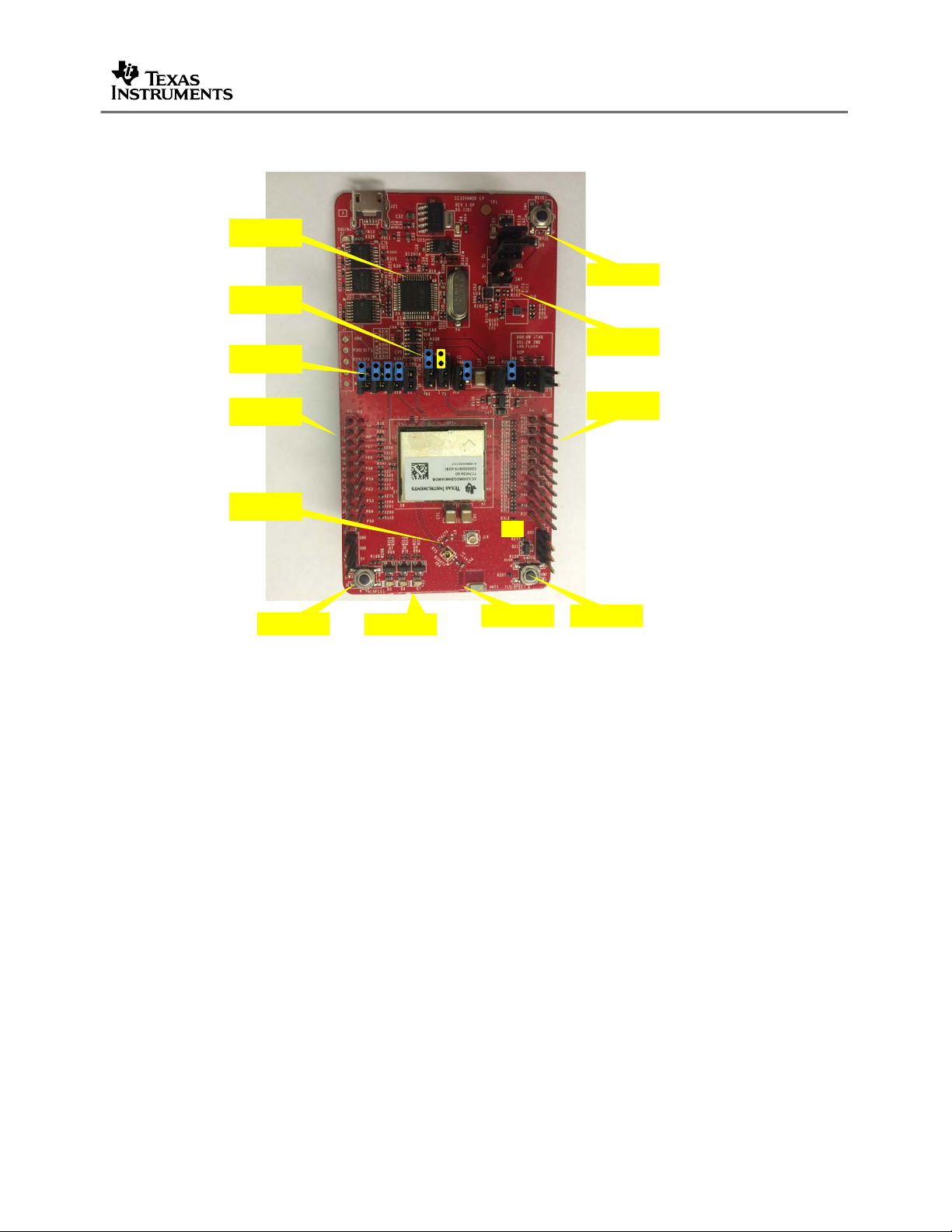
2 Hardware
U.FL
CC3200
Chip Antenna
User LEDs
Push Button
Push Button
Reset
JTAG
Headers
UART
Signals
20 pin
J1, J3
20 pin
J2, J4
Sensor
Area
FTDI
JTAG Emu
Murata
Conn
EVM User’s Guide
EVM Overview
TI Confidential – Strictly Private 4
Page 4
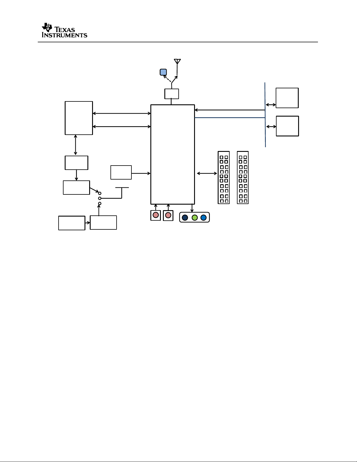
2.1 Block Diagram
FTDI
FT2232D
+
SWD circuit
CC3200MOD
USB
Conn
LDO
3.3V
2xAA
Batt Conn
Acc
BMA222
Temp
Sensor
TMP006
Chip
ant
I2C
LEDs
GPIO9,10,11
Push buttons
GPIO13, 22
2x20 Launchpad headers
(Compatible with TI MCU Std *)
M25PX80-VMN6TP
W25Q80BLUXIG
VCC
JTAG/SWD
UART (Flashing)
U.FL
Filter
Reverse
Protection
INT(GPIO13)
DC/DC
3.3V
VDD_FLASH
EVM User’s Guide
Block Diagram
2.2 Hardware features of the CC3200MOD Launchpad (Evaluation board)
• CC3200MOD Module with CC3200 device with RF filter, serial flash and crystal.
• Low-Power ARM Cortex M4 with 802.11 bgn WIFI
• 40-pin LaunchPad standard that leverages the BoosterPack ecosystem
• FTDI based JTAG emulation with Serial port for flash programming.
• Supports both 4 wire JTAG and 2 wire SWD
• Two buttons and three LEDs for user interaction
• Virtual COM port UART through USB on PC
• On-board chip antenna with U.FL for conducted testing.
• On-board Accelerometer and Temperature sensor for Out of Box demo with option to
isolate them from the I2C bus.
• Micro USB connector for power and debug connections.
TI Confidential – Strictly Private 5
Page 5

EVM User’s Guide
measurement
device.
(battery connector)
up to 0.4V)
in the reverse manner.
• Headers for current measurement and external JTAG connection.
• Bus powered device with no external power required for WIFI.
• Long range transmission with highly optimized antenna (200m Typical in open air with a
6dBi antenna AP)
• Can be powered with external 2xAA or 2xAAA alkaline batteries working down to 2.3V typ.
2.2.1 Power connections
The board can be powered by using the on-board micro USB connector. An on-board
LDO provides 3.3V for the CC3200 and the rest of the board to operate. This supply can
be isolated from the LDO using the jumpers on the board.
J12
J13 Board power Short: Supply the board power from the on-board
J19 5V power 5V output from the USB VBUS (has a diode drop of
J20 3.3V power
Various powering options are discussed in subsequent sections.
Current
input
Measure the current flowing into the CC3200
LDO.
Open : Supply the board power from the J20
Can be used to power the board from an external
2XAA battery pack. It has in-built reverse voltage
protection to prevent the battery from being plugged
2.2.2 2x20 pin connector assignment
The signal assignment on the 2x20 pin connector is shown below. The convention of J1..J4
is replaced with P1…P4 to avoid confusion with the actual board reference.
TI Confidential – Strictly Private 6
Page 6
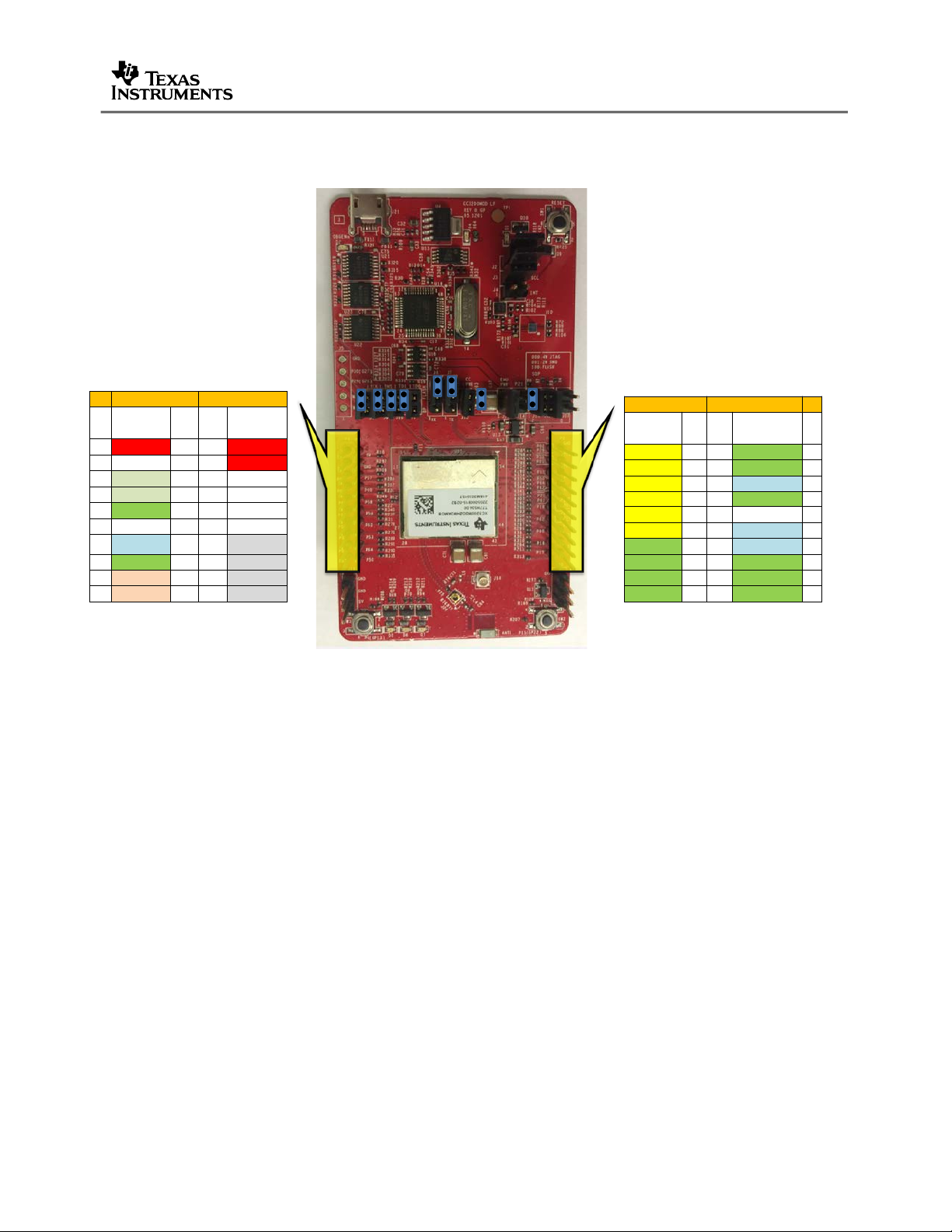
EVM User’s Guide
CC3200
P1 P3
Ref
Signal
Dev
Pin#
Dev
Pin#
Signal
1
3.3V
5V
2
ADC_CH1
58
GND
3
UART0_RX
4 57
ADC_CH0
4
UART0_TX
3 60
ADC_CH3
5
GPIO
61
58*
ADC_CH1
6
ADC_CH2
59
59*
ADC_CH2
7
SPI_CLK
5 63
AUD_SYNC
8
GPIO
62 53
AUD_CLK
9
I2C_SCL
1 64
AUD_DOUT
10
I2C_SDA
2 50
AUD_DIN
P4 P2
Signal
Dev
Pin#
Dev
Pin#
Signal
Ref
PWM
2*
GND
1
PWM1*18
GPIO
2
PWM
17*8SPI_CS
3
PWM
64*45GPIO
4
CCAP/GPIO
21*
RESET_OUT
5
CCAP/GPIO
18*7SPI_DOUT
6
GPIO
62*6SPI_DIN
7
GPIO
60*21GPIO
8
GPIO1655
GPIO
9
GPIO1715
GPIO
10
The signal mappings are as per the table above. All the signals are referred by the pin-no in the
SDK and the table above shows the default mappings. Note that some of the pins are repeated
across the connector. For e.g. pin 62 is available on P1 and P4, but only P1 is connected by
default. The signal on P4 is marked with a *(star) to signify that is not connected by default. It
can be routed to the pin by using a 0 Ohm resistor in the path. Please refer to the schematics
and placement diagram for the exact resistor placement.
2.3 Power
TI Confidential – Strictly Private 7
The Launchpad is designed to work from the USB provided power supply as it
enumerates as a bus-powered device. Care has been taken in the design to ensure that
the board does not violate the in-rush limits of the USB bus. The board can also be
powered by an external 2xAA or 2xAAA battery which is connected on J20.
Page 7

2.4 PCB Layout information
Figure 1 : TOP Layer
EVM User’s Guide
Figure 2 : Layer-2
TI Confidential – Strictly Private 8
Page 8

Figure 3 : Layer-3
EVM User’s Guide
Figure 4 : Bottom Layer
TI Confidential – Strictly Private 9
Page 9

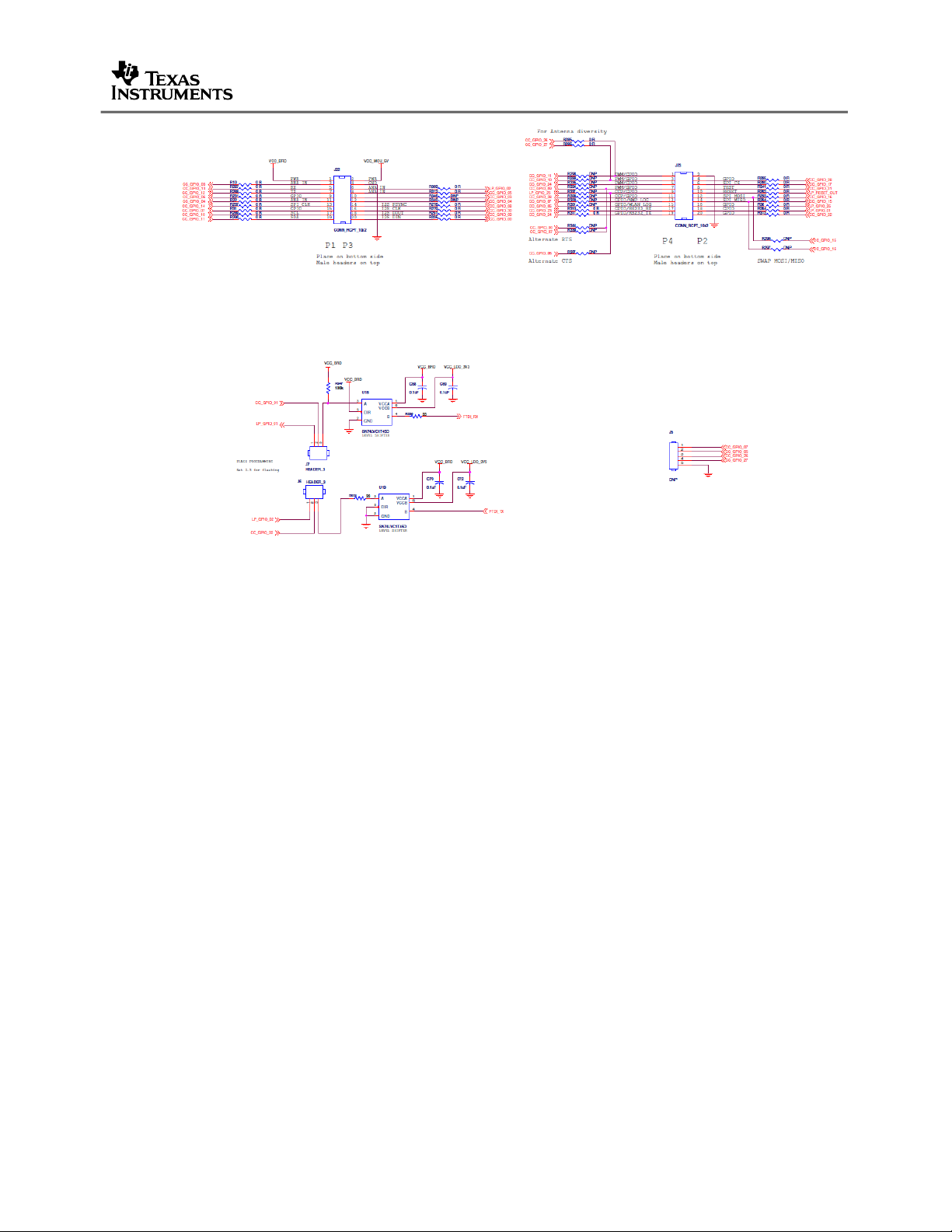
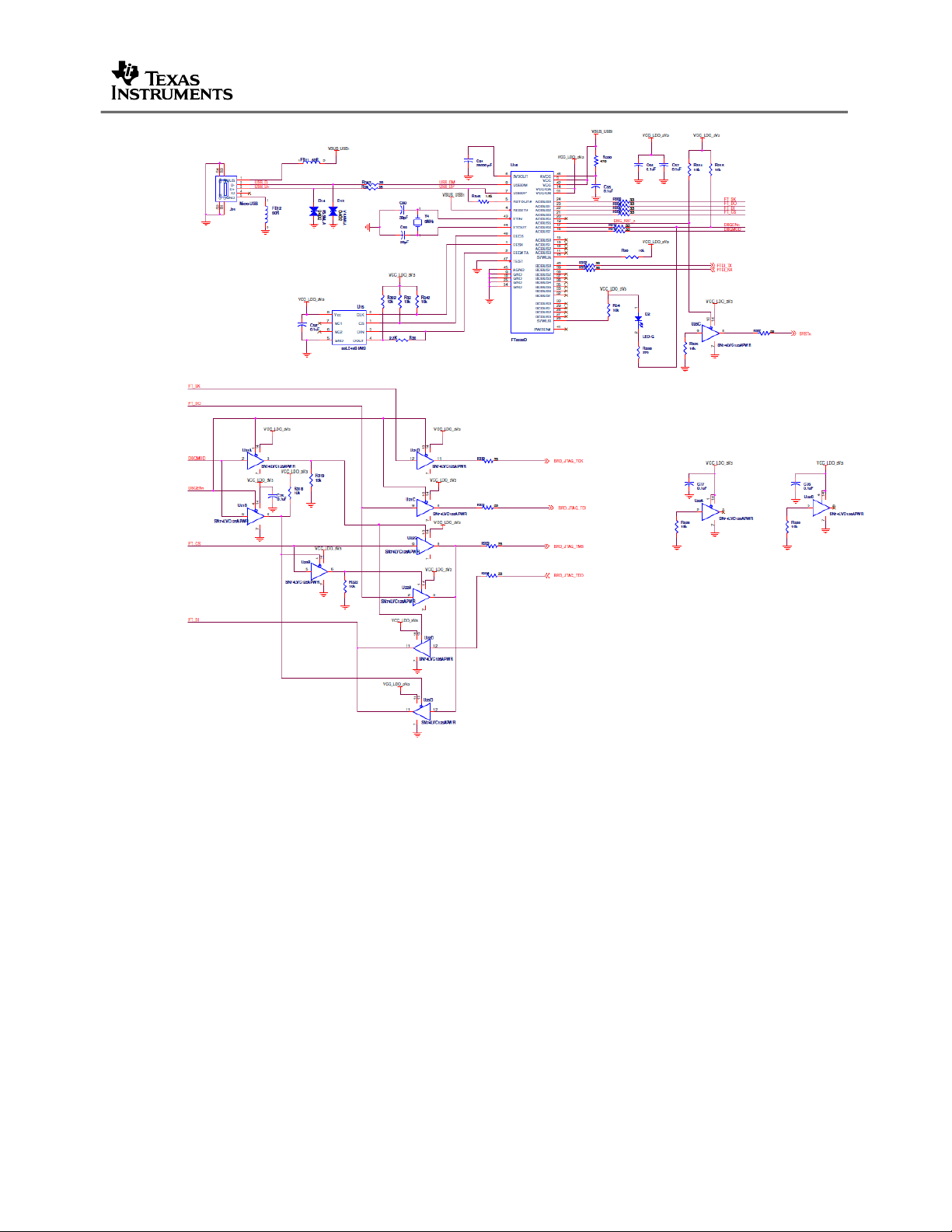
2.5 Schematics
EVM User’s Guide
TI Confidential – Strictly Private 10
Page 10
EVM User’s Guide
TI Confidential – Strictly Private 11
Page 11
EVM User’s Guide
TI Confidential – Strictly Private 12
Page 12

EVM User’s Guide
TI Confidential – Strictly Private 13
Page 13

EVM User’s Guide
TI Confidential – Strictly Private 14
Page 14

2.6 Bill of materials
NO. Value
Qty Description PCB Footprint Part Number
Manufacturer Mfr. PN Part Reference
1 0 R 43 RES C SM D 0402 0ohm 5% GP /HF R-0402S0 251.00681.025 Yageo
RC0402JR-070RL
R10 R12 R22 R31 R36 R75 R97 R98 R99
R101 R102 R103 R104 R106 R107 R108
R109 R110 R231 R237 R277 R278 R279
R280 R284 R285 R286 R287 R288 R289
R290 R291 R292 R293 R294 R295 R309
R310 R311 R312 R313 R335 R341
2
33nF 2 CA P CE R 33nF 10% 10V S MD 0402 GP/HF X7R T=0. 5mm C-0402S0 202.00095.005
MURATA GRM155R71A333KA01D C54 C62
3 0.1uF 14 CAP CER 100nF 10% 10V S MD 0402 GP/HF X5R 0.5mm C-0402S0 202.00008.015 Murata GRM155R61A104KA01D
C50 C51 C52 C55 C56 C57 C58 C68 C69
C70 C72 C75 C76 C77
4 1.0pF
1
CAP CE R 1.0pF +-0.25pF 50V SM D 0402 GP/HF NP O T=0. 55mm C-0402S0 202.00021.005
WALSIN
0402N1R0C500LT C64
5 1.5Kohm 1 RES C SMD 0402 1.5Kohm 5% GP/HF R-0402S0 251.00675.015 YAGEO RC0402JR-071K5L
R345
6 100uF
3 CAP CER 100uF 20% 6.3V S MD 1210 GP/HF X5R 2.5mm C-1210 205.00025.005
MURATA GRM32ER60J107ME20L C37 C65 C71
7
100k 8 RES C SMD 0402 100K ohm 1% GP /HF R-0402S0 261.00840.025
Yageo RC0402FR-07100KL R4 R7 R11 R212 R213 R214 R226 R347
8 100R 1 RES C SMD 0402 100ohm 5% GP/HF
R-0402S0 251.00004.005 Yageo RC0402JR-07100RL R225
9 10k 19 RES C SMD 0402 10Kohm 1% GP/HF R-0402S0 261.00839.035 Yageo RC0402FR-0710KL
R8 R30 R32 R34 R207 R208 R209 R210
R211 R302 R314 R315 R318 R319 R322
R325 R328 R329 R342
10 10pF
1 CAP CER 10pF + - 0.25pF 50V SM D 0402 GP/HF NP O 0.5mm C-0402S0 202.00035.005
WALSIN 0402N100C500LT C73
11
10uF 4 CA P CE R 10uF 20% 6.3V SM D 0603 GP/HF X5R T=0.8mm C-0603S0 203.00919.005 TDK C1608X5R0J106MT C32 C33 C63 C66
12 10uH 1 IND C 10uH 20% 100mA 0.6ohm SMD 0805 GP /HF
L-0805 130.00108.005 MURATA LQM21FN100M70L L11
13 15pF 1 CAP CER 15pF 5% 25V SMD 0402 GP/ HF NPO T =0.55mm C-0402S0 202.00052.005 WALS IN 0402N150J250LT C31
14 6MHz- XTAL -4 1 XTAL 6MHz 30ppm 20pF 150ohm SM D O-SMD49S12X4_8S0 TXC 9C06000086 Y4
15 1K 3 RES C SMD 0402 1Kohm 1% GP/HF R-0402S0 261.00835.025 Yageo RC0402FR-071KL
R9 R168 R169
16 2.2K
1 RES C SMD 0402 2.2Kohm 5% GP/HF R-0402S0 251.00014.025
WALSIN WR04X 222 J TL R35
17
270 6 RES C SMD 0402 270ohm 5% GP /HF R-0603S0 251.00025.025 Yageo/Phycomp. RC0402JR-07270RL R64 R69 R70 R94 R95 R326
18 30pF 2 CAP CER 30pF 5% 50V SMD 0402 GP/ HF NPO T=0.5mm
C-0402S0 202.01156.015
WALSIN 0402N300J500CT C59 C60
19 28ohm 2 RES C SMD 0402 28ohm 1% GP/HF R-0402S0 YAGEO RC0402FR-0728RL R28 R343
20 3.3K 2 RES C SMD 0402 3.3Kohm 5% GP/HF R-0402S0 251.00027.005 TA-I RM04JTN332 R172 R173
21 3.3M 1 RES C SMD 0402 3.3Mohm 5% GP/HF
R-0402S0
251.00689.005 TA-I
RM04JTN335 R118
22 3.6nH 1
IND C 3.6nH 0. 3nH 300mA 0.2ohm Q=8 SMD 0402 GP/ HF l-0402s0 130.01491.005 TAIYO HK10053N6S-T
L4
23 30.1K 1 RES C SMD 0402 30.1K ohm 1% GP /HF R-0402S0 261.00915.005
YAGEO RC0402FR-0730K1L R55
24 33ohm
15 RES C SM D 0402 33ohm 5% GP /HF R-0402S0 251.00657.015
Yageo RC0402JR-0733RL
R303 R304 R305 R306 R316 R317 R320
R321 R323 R324 R327 R330 R331 R332
R333
25 470ohm 1 RES C SMD 0402 470ohm 5% GP/HF
R-0402S0
251.00034.005 Yageo
RC0402JR-07470RL R338
26 52.3K 1
RES C SMD 0402 52.3Kohm 1% GP/ HF R-0402S0 261.00978.005 TA-I RM04FTN5232
R56
27 60R 2 BEA D C 60ohm 25% 4A 0.02ohm SMD 0603 GP/HF L-0603S0
151.00402.005
CHILISIN UPB160808T-600Y-N FB11 FB 12
28
93LC46B-I/MS 1
Serial EEPRO M 2.5-5.5V 16- bit word size SMD MSOP-8A
Microchip 93LC46BT-I/ST
U15
29 AH316M245001-T 1
2.4G wif i ANT ANT-S3_2X1_6-2A
Taiyo_Yuden AH316M245001-T
ANT1
30 BMA222
1 3-AXIS ACCELEROMETER DIGITAL SMD tlp-2x2-12 JSBMA220 Bosch
BMA222E U14
31
BSS138LT3G 4 MOSFET N-CH 50V 200MA SOT-23 sot-23b On Semi BSS138LT3G/BSS138LT1G Q7 Q8 Q9 Q10
32 CONN_MICRO_USB 1 CONN M ICRO USB B 5PIN 0.65mm SM D FEM ALE RT GP
CJ-USBSUA-160M3B-L2AT
342.00757.005 POWERWAY SUA-160M3B-L2E-TR1
J21
33 CONN_RCPT_10x2 2 CONN RCPT .100" 20POS DUAL TI N cn-10x2-2_54c
Samtec SSQ-110-03-T-D J22 J23
34 CONN_U.FL 1 HEADER RF 1*1P ORT D0.5/D2.0mm SMD MALE ST GP /HF CJ-RF-S3_1X3-3 341.00021.005
FOXCONN KK23017-01-7F
J18
35 DIODE 1 DIODE SBD 30V 1.0A SMD POWER DI123 GP/HF D-DFLT51AS0 112.00419.005 DIODES DFLS130L-7 D9
36 FT2232D
1
IC PER 4. 35~ 5.25V S MD LQFP48 GP USB CONTROLLER FT2232D
TQFP-48S0 JSFT2232D
FTDI FT2232D
U16
37
HEADER_3 5 HEADER PIN 3P 2.54mm DIP MALE ST GP CN-3X1-2_54
CVILUX
CH31032V200 J6 J7 J13 J19 J20
38 JUMPER MALE 12 HEADER PIN 1*2P 2.54mm DIP MALE ST GP
CN-D2X1-2_54S0
341.00391.005 CVILUX CH31022V202
J2 J3 J4 J8 J9 J 10 J 11 J 12 J14 J 15 J 16 J 17
39 LED_G 2
LED CHIP 35mcd G 571nm 2P SMD 1.6*0.8mm GP/HF LTST-C190
LD-0603S0 123.00170.005 LITEON LTST-C190KGKT
D2 D5
40 LED_R
2 LED CHIP 45~180mcd R 624~638nm 2P SMD 1.6*0.8mm GP/HF
LD-0603S0
123.00172.005 LITEON
LTST-C190KRKT
D4 D7
41 LED_Y 2
LED CHIP 60mcd O 605nm 2P SMD 1.6*0.8mm GP/HF LTST-C190
LD-0603A 123.00171.005 LITEON LTST-C190KFKT D1 D6
42 MM8030-2610RJ3
1 HEADER RF 1*1P ORT D=0. 5/1.35mm SMD F E MALE ST GP CN-MM8030S0 341.00454.005
MURATA MM8030-2610RJ3 J24
43 SI2323DS-T1-GE3
1 MOSFET P-CH 20V 3.7A SO T 23-3 sot-23b Vishay SI2323DS-T1-GE3 Q11
44 SN74LVC125APWR 2
IC BUFFERS 1.65~ 3.6V S MD TSSOP14 GP / HF SN74LVC125APW R
SSOP-14S0 075.00394.005 TI SN74LVC125APWRG4
U21 U23
45 SN74LVC126APWR 1
IC CM OS 1.65~3.6V S MD TSSOP14 GP /HF SN74LVC126APWR SSOP-14S0 075.00289.005 TI
SN74LVC126APWR U22
46 SN74LVC1T45D
2
IC TRANSCEIVER 1. 65~ 5. 5V SMD SOT 23- 6 GP/HF SN74LVC1T 45D
M-SOT-23-6
082.00020.005 TI SN74LVC1T45DBVR U18 U19
47 SW-4PIN 3 SW TACT 50mA 12V SMD ST GP/HF SW-1BT002S1 182.00083.005
FOXCONN 1BT002-0120L-7H SW1 SW2 SW3
48 TMP006 1 IC SENSOR THERMOPILE 8DSBGA tbga-3x3-8c TI TMP006AIYZFR U10
49 TPS61097-33DBVR 1 IC REG BST SYNC 3.3V .1A SOT23-5 SOT_23_5 027.01039.005 TI TPS61097-33DBVT U13
50 TPS73701 1 IC REG 1.2~ 5.5V 1A SMD SOT 223- 6 GP/HF TPS73701DCQR sot-223-6 027.00812.005 TI TPS73701DCQR
U4
51 V5.5MLA 2 VARISTO R 5.5V 20A 2P SMD 0402 GP R-0402S0 170.00089.005 L ITTELFUSE V5.5MLA0402NR D13 D14
52 PCB 1 81.3mm*50.3mm, 4 layers, thr ough hole 308.01741.005
ZHENDING 308.01741.005
53 Module 1 Module, 802. 11bgn 1x1, 17.5mmx20.5mm LGA T77H534.00 FOXCONN T77H534.00
U11
EVM User’s Guide
TI Confidential – Strictly Private 15
Page 15

2.7 Antenna information
EVM User’s Guide
TI Confidential – Strictly Private 16
Page 16

EVM User’s Guide
STANDARD TERMS AND CONDITIONS FOR EVALUATION MODULES
1. Delivery: TI delivers TI evaluation boards, kits, or modules, including any accompanying demonstration software, com ponents, or
documentation (collectively, an “EVM” or “EVMs”) to the User (“User”) in accordance with the terms and conditions set forth herein.
Acceptance of the EVM is expressly subject to the following terms and conditions
1.1 EVMs are intended solely for product or software developers for use in a research and development setting to facilitate feasibility
evaluation, experimentation, or scientific analysis of TI semiconductors products. EV Ms have no direct function and are not
finished products. EVMs shall not be directly or indirectly assembled as a part or subassembly in any finished product. For
clarification, any software or software tools provided with the EVM (“Software”) shall not be subject to the terms and conditions
set forth herein but rather shall be subject to the applicable terms and conditions that accompany such Software
1.2 EVMs are not intended for consumer or household use. EVMs may not be sold, sublicensed, leased, rented, loaned, assigned,
or otherwise distributed for commercial purposes by Users, in whole or in part, or used in any finished product or production
system.
2 Limited Warranty and Related Remedies/Disclaimers:
2.1 These terms and conditions do not apply to Software. The warranty, if any, for Software is covered in the applicable Software
License Agreement.
2.2 TI warrants that the TI EVM will conform to TI's published specifications for ninety (90) days after the date TI delivers such EVM
to User. Notwithstanding the foregoing, TI shall not be liable for any defects that are caused by neglect, misuse or mistreatment
by an entity other than TI, including improper installation or testing, or for any EVMs that have been altered or modified in any
way by an entity other than TI. Moreover, TI shall not be liable for any defects that result from User's design, specifications or
instructions for such EVMs. Testing and other quality control techniques are used to the extent TI deems necessary or as
mandated by government requirements. TI does not test all parameters of each EVM.
2.3 If any EVM fails to conform to the warranty set forth above, TI's sole liability shall be at its option to repair or replace such EVM,
or credit User's account for such EVM. TI's liability under this warranty shall be limited to EVMs that are returned during the
warranty period to the address designated by TI and that are determined by TI not to conform to such warranty. If TI elects to
repair or replace such EVM, TI shall have a reasonable time to repair such EVM or provide replacements. Repaired EVMs shall
be warranted for the remainder of the original warranty period. Replaced EVMs shall be warranted for a new full ninety (90) day
warranty period.
3 Regulatory Notices:
3.1 United States
3.1.1 Notice applicable to EVMs not FCC-Approved:
This kit is designed to allow product developers to evaluate electronic components, circuitry, or software associated with the kit
to determine whether to incorporate such items in a finished product and software developers to write software applications for
use with the end product. This kit is not a finished product and when assembled may not be resold or otherwise marketed unless
all required FCC equipment authorizations are first obtained. Operation is subject to the condition that this product not cause
harmful interference to licensed radio stations and that this product accept harmful interferenc e. Unless the assembled kit is
designed to operate under part 15, part 18 or part 95 of this chapter, the operator of the kit must operate under the authority of
an FCC license holder or must secure an experimental authorization under part 5 of this chapter.
3.1.2 For EVMs annotated as FCC – FEDERAL COMMUNICATIONS COMMISSION Part 15 Compl i a nt:
CAUTION
This device complies with part 15 of the FCC Rules. Operation is subject to the following two conditions: (1) This device may not
cause harmful interference, and (2) this device must accept any interference received, including interference that may cause
undesired operation.
Changes or modifications not expressly approved by the party responsible for compliance could void the user's authority t o
operate the equipment.
FCC Interference Statement for Class A EVM devices
NOTE: This equipment has been tested and found to comply with the limits for a Class A digital device, pursuant to part 15 of
the FCC Rules. These limits are designed to provide reasonable protection against harmful interference when the equipment is
operated in a commercial environment. This equipment generates, uses, and can radiate radio frequency energy and, if not
installed and used in accordance with the instruction manual, may cause harmful interference to radio communications.
Operation of this equipment in a residential area is likely to cause harmful interference in which case the user will be required to
correct the interference at his own expense.
FCC Interference Statement for Class B EVM devices
NOTE: This equipment has been tested and found to comply with the limits for a Class B digital device, pursuant to part 15 of
the FCC Rules. These limits are designed to provide reasonable protection against harmful interference in a residential
installation. This equipment generates, uses and can radiate radio frequency energy and, if not installed and used in accordance
with the instructions, may cause harmful interference to radio communications. However, there is no guarantee that interferenc e
will not occur in a particular installation. If this equipment does cause harmful interference to radio or television reception, which
can be determined by turning the equipment off and on, the user is encouraged to try to correct the interference by one or more
of the following measures:
• Reorient or relocate the receiving antenna.
• Increase the separation between the equipment and receiver.
• Connect the equipment into an outlet on a circuit different from that to which the receiver is connected.
• Consult the dealer or an experienced radio/TV technician for help.
TI Confidential – Strictly Private 17
Page 17

EVM User’s Guide
3.2 Canada
3.2.1 For EVMs issued with an Industry Canada Certificate of Conformance to RSS-210
Concerning EVMs Including Radio Transmitters:
This device complies with Industry Canada license-exempt RSS standard(s). Operation is subject to the following two conditions:
(1) this device may not cause interference, and (2) this device must accept any interference, including interference that may
cause undesired operation of the device.
Concernant les EVMs avec appareils radio:
Le présent appareil est conforme aux CNR d'Industrie Canada applicables aux appareils radio exempts de licence. L'exploitati on
est autorisée aux deux conditions suivantes: (1) l'appareil ne doit pas produire de brouillage, et (2) l'utilisateur de l'appareil doit
accepter tout brouillage radioélectrique subi, même si le brouillage est susceptible d'en compromettre le fonctionnement.
Concerning EVMs Including Detachable Antennas:
Under Industry Canada regulations, this radio transmitter may only operate using an antenna of a type and maximum (or lesser)
gain approved for the transmitter by Industry Canada. To reduce potential radio interference to other users, the antenna type
and its gain should be so chosen that the equivalent isotropically radiated power (e.i.r.p.) is not more than that necessary for
successful communication. This radio transmitter has been approved by Industry Canada to operate with the antenna types
listed in the user guide with the maximum permissible gain and required antenna impedance for each antenna type indicated.
Antenna types not included in this list, having a gain greater than the maximum gain indicated for that type, are strictly prohibited
for use with this device.
Concernant les EVMs avec antennes détachables
Conformément à la réglementation d'Industrie Canada, le présent émetteur radio peut fonctionner avec une antenne d'un type et
d'un gain maximal (ou inférieur) approuvé pour l'émetteur par Industrie Canada. Dans le but de réduire les risques de brouillage
radioélectrique à l'intention des autres utilisateurs, il faut choisir le type d'antenne et son gain de sorte que la puiss ance isot rope
rayonnée équivalente (p.i.r.e.) ne dépasse pas l'intensité nécessaire à l'établissement d'une communication sat is f ais ant e. Le
présent émetteur radio a été approuvé par Industrie Canada pour fonctionner avec les types d'antenne énumérés dans le
manuel d’usage et ayant un gain admissible maximal et l'impédance requise pour chaque type d'antenne. Les types d'antenne
non inclus dans cette liste, ou dont le gain est supérieur au gain maximal indiqué, sont strictement interdits pour l'exploitation de
l'émetteur
3.3 Japan
3.3.1 Notice for EVMs delivered in Japan: Please see http://www.tij.co.jp/lsds/ti_ja/general/eStore/notice_01.page 日本国内に
輸入される評価用キット、ボードについては、次のところをご覧ください。
http://www.tij.co.jp/lsds/ti_ja/general/eStore/notice_01.page
3.3.2 Notice for Users of EVMs Considered “Radio Frequency Products” in Japan: EVMs entering Japan are NOT certified by
TI as conforming to Technical Regulations of Radio Law of Japan.
If User uses EVMs in Japan, User is required by Radio Law of Japan to follow the instructions below with respect to EVMs:
1. Use EVMs in a shielded room or any other test facility as defined in the notification #173 issued by Ministry of Internal
Affairs and Communications on March 28, 2006, based on Sub-section 1.1 of Article 6 of the Ministry’s Rule for
Enforcement of Radio Law of Japan,
2. Use EVMs only after User obtains the license of Test Radio Station as provided in Radio Law of Japan with respect to
EVMs, or
3. Use of EVMs only after User obtains the Technical Regulations Conformity Certification as provided in Radio Law of Japan
with respect to EVMs. Also, do not transfer EVMs, unless User gives the same notice above to the transferee. Please note
that if User does not follow the instructions above, User will be subject to penalties of Radio Law of Japan.
SPACER
【無線電波を送信する製品の開発キットをお使いになる際の注意事項】
本開発キットは技術基準適合証明を受けておりません。
本製品のご使用に際しては、電波法遵守のため、以下のいずれかの措置を取っていただく必要がありますのでご注意ください。
1. 電波法施行規則第6条第1項第1号に基づく平成18年3月28日総務省告示第173号で定められた電波暗室等の試験設備でご使用
いただく。
2. 実験局の免許を取得後ご使用いただく。
3. 技術基準適合証明を取得後ご使用いただく。
なお、本製品は、上記の「ご使用にあたっての注意」を譲渡先、移転先に通知しない限り、譲渡、移転できないものとします。
上記を遵守頂けない場合は、電波法の罰則が適用される可能性があることをご留意ください。
日本テキサス・インスツルメンツ株式会社
東京都新宿区西新宿6丁目24番1号
西新宿三井ビル
3.3.3 Notice for EVMs for Power Line Communication: Please see http://www.tij.co.jp/lsds/ti_ja/general/eStore/notice_02.page
電力線搬送波通信についての開発キットをお使いになる際の注意事項については、次のところをご覧くださ
い。http://www.tij.co.jp/lsds/ti_ja/general/eStore/notice_02.page
SPACER
4 EVM Use Restrictions and Warnings:
4.1 EVMS ARE NOT FOR USE IN FUNCTIONAL SAFETY AND/OR SAFETY CRITICAL EVALUATIONS, INCLUDING BUT NOT
LIMITED TO EVALU A T IO NS OF LIFE SUPPORT APPLICATIONS.
4.2 User must read and apply the user guide and other available documentation provided by TI regarding the EVM prior to handling
TI Confidential – Strictly Private 18
Page 18

EVM User’s Guide
or using the EVM, including without limitation any warning or restriction notices. The notices contain important safet y informat ion
related to, for example, temperatures and voltages.
4.3 Safety-Related Warnings and Restrictions:
4.3.1 User shall operate the EVM within TI’s recommended specifications and environmental considerations stated in the user
guide, other available documentation provided by TI , and any ot her appl icabl e requirem ents and em ploy reasonable and customary
safeguards. Exceeding the specif ied perform ance ratings and specifications (including but not limited to input
and output voltage, current, power, and environmental ranges) for the EVM may cause personal injury or death, or
property damage. If there are questions concerning performance ratings and specifications, User should contact a TI
field representative prior to connecting interface electronics including input power and intended loads. Any loads applied
outside of the specified output range may also result in unintended and/or inaccurate operation and/or possible
permanent damage to the EVM and/or interface electronics. Please consult the EVM user guide prior to connecting any
load to the EVM output. If there is uncertainty as to the load specific ati on, please cont act a TI field represent ative.
During normal operation, even with the inputs and outputs kept within the specified allowable ranges, some circuit
components may have elevated case temperatures. These components include but are not limited to linear regulators,
switching transistors, pass transistors, current sense resistors, and heat sinks, which can be identifi ed using the
information in the associated documentation. When working with the EVM, please be aware that the EVM ma y become
very warm.
4.3.2 EVMs are intended solely for use by technically qualified, professional electronics experts who are familiar with t he
dangers and application risks associated with handling electrical mechanical components , systems, and subsystems.
User assumes all responsibility and liability for proper and safe handling and use of the EVM by User or its employees,
affiliates, contractors or designees. User assumes all responsibility and liabil ity t o ensure that any interfaces (el ect ronic
and/or mechanical) between the EVM and any human body are designed with suitable isolation and means to safely
limit accessible leakage currents to minimize the risk of electrical shock hazard. User assumes all responsibility and
liability for any improper or unsafe handling or use of the EVM by User or its employees, affiliates, contractors or
designees.
4.4 User assumes all responsibility and liability to determine whether the EVM is subject to any applicable international, federal,
state, or local laws and regulations related to User’s handling and use of the EVM and, if applicable, User assumes all
responsibility and liability for compliance in all respects with such laws and regulations. User assumes all responsibility and
liability for proper disposal and recycling of the EVM consistent with all applicable international, federal, st at e, and local
requirements.
5. Accuracy of Information: To the extent TI provides information on the availability and functi on of EVMs, TI attempts to be as
accurate as possible. However, TI does not warrant the accuracy of EVM descript ions, EVM availability or other inform ation on its
websites as
accurate, complete, reliable, current, or error-free.PACER
6. Disclaimers:
6.1 EXCEPT AS SET FORTH ABOVE, EVMS AND ANY WRITTEN DESIGN MATERIALS PROVIDED WITH THE EVM (AND THE
DESIGN OF THE EVM ITSELF) ARE PROVIDED "AS IS" AND "WITH ALL FAULTS." TI DISCLAIMS ALL OTHER
WARRANTIES, EXPRESS OR IMPLIED, REGARDING SUCH ITEMS, INCLUDING BUT NOT LIMITED TO ANY IMPLIED
WARRANTIES OF MERCHANTABILITY OR FITNESS FOR A PARTICULAR PURPOSE OR NON-INFRINGEMENT OF ANY
THIRD PARTY PATENTS, COPYRIGHTS, TRADE SECRE TS OR OTHER INTE L LECT UA L PROPERT Y RIG HT S.
6.2 EXCEPT FOR THE LIMITED RIGHT TO USE THE EVM SET FORTH HEREIN, NOTHING I N THESE TERMS AND
CONDITIONS SHALL BE CONSTRUED AS GRANTING OR CONFERRING ANY RIGHTS BY LICENSE, PATENT, OR ANY
OTHER INDUSTRIAL OR INTELLECTUA L PROPE RTY RIGHT OF TI, I TS SUPPL IE RS/ L ICENSORS OR ANY OTHER THIRD
PARTY, TO USE THE EVM IN ANY FINISHED END-USER OR READY-TO-USE FINAL PRODUCT, OR FOR ANY
INVENTION, DISCOVERY OR IMPROVEMENT MA DE, CONCE IVED OR ACQUIRED PRIOR TO OR AFTER DELIVERY OF
THE EVM.
7. USER'S INDEMNITY OBLIGATIONS AND REPRESE NT ATIONS. USER WILL DEFEND, INDEMNIFY AND HOLD TI, ITS
LICENSORS AND THEIR REPRESENTATIVES HARMLESS FROM AND AGAINST ANY AND ALL CLAIMS, DAMAGES,
LOSSES,
EXPENSES, COSTS AND LIABILITIES (COLLECTIVELY, "CLAIMS") ARISING OUT OF OR IN CONNECTION WITH ANY
HANDLING OR USE OF THE EVM THAT IS NOT IN ACCORDANCE WITH THESE TERMS AND CONDITIONS. THIS
OBLIGATION
SHALL APPLY WHETHER CLAIMS ARISE UNDE R STAT UTE, REGULATION, OR THE LAW OF TORT, CONTRACT OR ANY
OTHER LEGAL THEORY, AND EVEN IF THE EVM FAILS TO PERFORM AS DESCRIBED OR EXPECTED.
8. Limitations on Damages and Liability:
8.1 General Limitations. IN NO EVENT SHALL TI BE LIABLE FOR ANY SPECIAL, COLLATERAL, INDIRECT, PUNITIVE,
INCIDENTAL, CONSEQUENTIAL, OR EXEMPLA RY DA MA GES I N CONNECTI ON W ITH OR ARISI NG OUT OF THESE
TERMS ANDCONDITIONS OR THE USE OF THE EVMS PROVIDED HEREUNDE R, RE GARDLESS OF WHETHER TI HAS
BEEN ADVISED OF THE POSSIBILITY OF SUCH DAMAGES. EXCLUDED DAMAGES INCLUDE, BUT ARE NOT LIMITED
TO, COST OF REMOVAL OR REINSTALLATION, ANCILLARY COSTS TO THE PROCUREMENT OF SUBSTITUTE GOODS
OR SERVICES, RETESTING, OUTSIDE COMPUTER TIME, LABOR COSTS, LOSS OF GOODWILL, LOSS OF PROFITS,
LOSS OF SAVINGS, LOSS OF USE, LOSS OF DATA, OR BUSINESS INTERRUPTION. NO CLAIM, SUIT OR ACTION SHALL
BE BROUGHT AGAINST TI MORE THAN ONE YEAR AFTER THE RELATED CAUSE OF ACTION HAS OCCURRED.
8.2 Specific Limitations. IN NO EVENT SHALL TI'S AGGREGATE LIABILITY FROM ANY WARRANTY OR OTHER OBLIGATION
ARISING OUT OF OR IN CONNECTION WITH THESE TERMS AND CONDITIONS, OR ANY USE OF ANY TI EVM
TI Confidential – Strictly Private 19
Page 19

EVM User’s Guide
PROVIDED HEREUNDER, EXCEED THE TOTAL AMOUNT PAI D TO T I FO R THE PARTICULAR UNITS SOLD UNDER
THESE TERMS AND CONDITIONS WITH RESPECT TO WHICH LOSSES OR DAMAG ES ARE CLA IMED. THE EXISTENCE
OF MORE THAN ONE CLAIM AGAINST THE PARTICULAR UNITS SOLD TO USER UNDER THESE TERMS AND
CONDITIONS SHALL NOT ENLARGE OR EXTEND THIS LIMIT.
9. Return Policy. Except as otherwise provided, TI does not offer any refunds, returns, or exchanges. Furtherm ore, no return of
EVM(s)
will be accepted if the package has been opened and no return of the EVM(s) will be accepted if they are damaged or otherwise not
in
a resalable condition. If User feels it has been incorrectly charged for the EVM(s) it ordered or that delivery violates the applicable
order, User should contact TI. All refunds will be made in full within thirty (30) working days from the return of the components(s),
excluding any postage or packaging costs.
10. Governing Law: These terms and conditions shall be governed by and interpreted in accordance with the laws of the State of
Texas,
without reference to conflict-of-laws principles. User agrees that non-exclusive jurisdiction for any dispute arising out of or relati ng to
these terms and conditions lies within courts located in the State of Texas and consents to venue in Dallas County, Texas.
Notwithstanding the foregoing, any judgment may be enforced in any United States or foreign court, and TI may seek injunctive
reliefin any United States or foreign court.
spacer
__
Mailing Address: Texas Instruments, Post Office Box 655303, Dallas, Texas 75265
Copyright © 2014, Texas Instruments Incorporated
TI Confidential – Strictly Private 20
 Loading...