


TI CC3000 Evaluation Module
User's Guide
Literature Number: SWRU326
November 2012

Contents
Preface ....................................................................................................................................... 4
1 Introduction ........................................................................................................................ 5
2 CC3000 EM Board ............................................................................................................... 6
2.1 EM Board Top View ........................................................................................................ 6
2.2 EM Board Bottom View .................................................................................................... 9
2.3 Antenna ..................................................................................................................... 10
2.4 Hardware Setup ........................................................................................................... 13
2.5 Schematics ................................................................................................................. 14
2.6 Bill of Materials (BOM) .................................................................................................... 15
3 Layout Guidelines ............................................................................................................. 16
4 Application Development ................................................................................................... 21
2
Contents SWRU326–November 2012
Copyright © 2012, Texas Instruments Incorporated
Submit Documentation Feedback

www.ti.com
2-1. CC3000 EM Board Top View.............................................................................................. 6
2-2. CC3000 EM Board Bottom View.......................................................................................... 9
2-3. Antenna Location and RF Trace Routing .............................................................................. 10
2-4. Matching Circuit Between the Antenna and the CC3000 EM Board ............................................... 11
2-5. Return Loss from the ACX Antenna and Matching Circuit........................................................... 11
2-6. Antenna Radiation Patterns.............................................................................................. 12
2-7. Host PCB Mating Connector Arrangement ............................................................................ 13
2-8. Schematics of the CC3000 EM Board.................................................................................. 14
3-1. Module Layout Guidelines................................................................................................ 16
3-2. Module Layout Guidelines................................................................................................ 17
3-3. Trace Design for the PCB Layout ....................................................................................... 18
3-4. Layer 1 Combined With Layer 2......................................................................................... 18
3-5. Antenna and RF Trace Routing Layout Guidelines................................................................... 19
3-6. Power Supply Routing of the CC3000 EM Board..................................................................... 20
4-1. MSP-EXP430FR5739 Test Platform and CC3000 EM Board....................................................... 21
2-1. Key Parts of CC3000 EM Board Top View.............................................................................. 7
2-2. J2 Configuration of the CC3000 EM Board.............................................................................. 7
2-3. Header J4 of the CC3000 EM Board Top View......................................................................... 7
2-4. Header J5 of the CC3000 EM Board Top View......................................................................... 8
2-5. Header J6 of CC3000 EM Board Bottom View ......................................................................... 9
2-6. J7 of CC3000 EM Board Bottom View................................................................................... 9
2-7. BOM for the TI CC3000 EM Board...................................................................................... 15
3-1. Module Layout Guidelines................................................................................................ 17
3-2. Trace Design Measurement Values .................................................................................... 18
3-3. Antenna and RF Trace Routing Layout Guidelines................................................................... 19
List of Figures
List of Tables
SWRU326–November 2012 List of Figures
Submit Documentation Feedback
Copyright © 2012, Texas Instruments Incorporated
3

About This Manual
This user guide describes how to use the TI CC3000 evaluation module (EM) board to evaluate the
performance of the TI CC3000 module.
Related Documentation From Texas Instruments
• TI SimpleLink™ CC3000 Module – Wi-Fi 802.11b/g Network Processor Data Sheet (SWRS126)
• CC3000 Wiki for MCU: http://processors.wiki.ti.com/index.php/CC3000_Wi-Fi_for_MCU
If You Need Assistance
The primary sources of CC3000 information are the device-specific data sheets and user’s guides. For the
most up-to-date version of the user’s guide and data sheets, go to http://www.ti.com/product/cc3000.
FCC Warning
This equipment is intended for use in a laboratory test environment only. It generates, uses, and can
radiate radio frequency energy and has not been tested for compliance with the limits of computing
devices pursuant to subpart J of part 15 of FCC rules, which are designed to provide reasonable
protection against radio frequency interference. Operation of this equipment in other environments may
cause interference with radio communications, in which case the user at his own expense will be required
to take whatever measures may be required to correct this interference.
Preface
SWRU326–November 2012
Read This First
4
Read This First SWRU326–November 2012
Copyright © 2012, Texas Instruments Incorporated
Submit Documentation Feedback

Chapter 1
SWRU326–November 2012
Introduction
This user guide describes how to use the TI CC3000 evaluation module (EM) board to evaluate the
performance and functionality of the TI CC3000 module. The CC3000 module is a self-contained Wi-Fi
®
solution that enables internet connectivity for a wide variety of microcontroller (MCU) systems. The
SimpleLink Wi-Fi from TI minimizes the host MCU software requirements, making it ideal for low-power
and low-cost applications. The CC3000 EM board is targeted for TI MCUs, such as the MSP430-FR5739
and other various host platforms. This document details the key parts and features of the CC3000 EM
board and the different options available to the user. This document includes layout guidelines to assist
the designer in PCB development.
SimpleLink is a trademark of Texas Instruments.
Wi-Fi is a registered trademark of Wi-Fi Alliance.
SWRU326–November 2012 Introduction
Submit Documentation Feedback
Copyright © 2012, Texas Instruments Incorporated
5
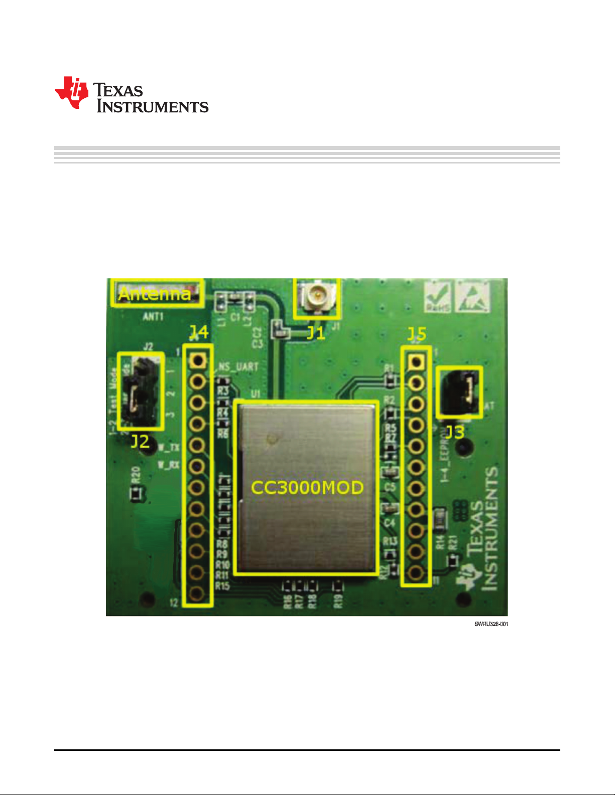
This section describes the key parts and features of the CC3000 EM board top and bottom views.
2.1 EM Board Top View
Figure 2-1 shows the key parts and jumpers mounted on the top of the CC3000 EM board. Table 2-1
describes the key parts of the EM board. Table 2-2 describes the J2 configuration of the CC3000 EM
board. Table 2-3 and Table 2-4 describe the J4 and J5 signals, respectively.
Chapter 2
SWRU326–November 2012
CC3000 EM Board
Figure 2-1. CC3000 EM Board Top View
6
CC3000 EM Board SWRU326–November 2012
Copyright © 2012, Texas Instruments Incorporated
Submit Documentation Feedback

www.ti.com
(1)
EM Board Top View
Table 2-1. Key Parts of CC3000 EM Board Top View
Key Parts Descriptions
CC3000MOD Core module for performance evaluation (for more information, see the CC3000
Antenna Can be used for radiated testing by reworking the capacitor to correct pads
J1 U.FL RF connector used for conductive RF test
J2 Used to switch between test mode and operation mode. When pins 2 and 3 are
J3 Used to test power consumption. The pins of the jumper are shorted in operation
J4 Through-hole test points (For more information, see Table 2-3.)
J5 Through-hole test points (For more information, see Table 2-4.)
module data sheet).
shorted, J2 runs in operation mode. When pins 1 and 2 are shorted, J2 runs in test
mode.
mode. For power testing, the jumper is removed and an ammeter bridges the pins.
Table 2-2. J2 Configuration of the CC3000 EM Board
Mode Description
Test mode: CC3000 radio tool
Functional mode: Normal mode Connect pins 2 and 3. Normal mode is for regular functionality between the host
For more information about test software for the PC, go to the CC3000 wiki at
http://processors.wiki.ti.com/index.php/CC3000_Wi-Fi_for_MCU.
(1)
Connect pins 1 and 2. Test mode is used with the CC3000 radio tool for operating,
testing, and calibrating the CC3000 chip-set designs during development. This tool
uses the RS232/UART pins to run radio frequency (RF) RX and TX tests on the
CC3000 module. For more information, see the CC3000 wiki.
platform and the CC3000 module.
Table 2-3. Header J4 of the CC3000 EM Board Top View
J4 Pin Pin Name Pin Type Descriptions
1 GND – Ground
2 Reserved – Reserved
3 Reserved – Reserved
4 Reserved – Reserved
5 WL_RS232_TX Output RS232 transmit output; used for the radio tool serial
6 WL_RS232_RX Input RS232 receive output; used for the radio tool serial
7 GND – Ground
8 WL_SPI_CS Input Host interface SPI chip select
9 WL_SPI_DOUT Output Host interface SPI data output
10 WL_SPI_IRQ Output Host interface SPI interrupt request
11 WL_SPI_DIN Input Host interface SPI data input
12 WL_SPI_CLK Input Host interface SPI clock input
interface in test mode. Leave floating in functional mode.
interface in test mode. Leave floating in functional mode.
SWRU326–November 2012 CC3000 EM Board
Submit Documentation Feedback
Copyright © 2012, Texas Instruments Incorporated
7
EM Board Top View
J5 Pin Pin Name Pin Type Descriptions
1 SCL_CC3000
2 SCL_EEPROM
3 SDA_CC3000
4 SDA_EEPROM
5 VBAT_SW_EN Input Active-high enables the signal from the host device.
6 GND – Ground
7 GND – Ground
8 VIO_HOST Power In VIO power supply from the host to the module. For the
9 VBAT_IN Power In Battery voltage input to module. For the MSP430 host
10 GND – Ground
11 Reserved – Reserved
(1)
The EM board arrives with EEPROM preprogrammed.
Table 2-4. Header J5 of the CC3000 EM Board Top View
(1)
(1)
(1)
(1)
Output I2C clock signal output from the CC3000 module. This
pin is connected to SCL_EEPROM through a 0-Ω
resistor and is not used by end users.
Input I2C clock signal input from EEPROM inside the CC3000
module. This pin is connected to SCL_CC3000 using a
0-Ω resistor and is not used by end users.
Input/Output I2C data signal from the CC3000 module. This pin is
connected to SDA_EEPROM using a 0-Ω resister and is
not used by end users.
Input/Output I2C data signal from EEPROM inside the CC3000
module. This pin is connected to the SDA_CC3000
device using a 0-Ω resistor and is not used by end users.
MSP430 host platform, VIO_HOST = VBAT_IN. For other
platforms that have different voltage levels from battery
voltages, R14 can be removed.
platform, VIO_HOST = VBAT_IN. For other platforms
that have different voltage levels from the battery
voltages, R14 can be removed.
www.ti.com
8
CC3000 EM Board SWRU326–November 2012
Copyright © 2012, Texas Instruments Incorporated
Submit Documentation Feedback

SWRU326-002
www.ti.com
2.2 EM Board Bottom View
The two EM board mating connectors J6 and J7 connect to the host platform and are mounted on the
bottom of the EM board, as shown in Figure 2-2. Table 2-5 and Table 2-6 describe the signals brought out
from these two EM mating connectors.
EM Board Bottom View
Figure 2-2. CC3000 EM Board Bottom View
Table 2-5. Header J6 of CC3000 EM Board Bottom View
J6 Pin Pin Name Module Pin Type Description
1 GND – Ground
5 Reserved – Reserved
10 VBAT_SW_EN Input Active-high enable signal from the host device
12 WL_SPI_IRQ Output Host interface SPI interrupt request
14 WL_SPI_CS Input Host interface SPI CS
16 WL_SPI_CLK Input Host interface SPI clock input
18 WL_SPI_DIN Input Host Interface SPI data input
19 GND – Ground
20 WL_SPI_DOUT Output Host interface SPI data output
Table 2-6. J7 of CC3000 EM Board Bottom View
J7 Pin Pin Name Module Pin Type Description
2 GND – Ground
7 VBAT_IN Power In Battery voltage input to the module
9 VBAT_IN Power In Battery voltage input to the module
15 Reserved – Reserved
SWRU326–November 2012 CC3000 EM Board
Submit Documentation Feedback
Copyright © 2012, Texas Instruments Incorporated
9

Antenna
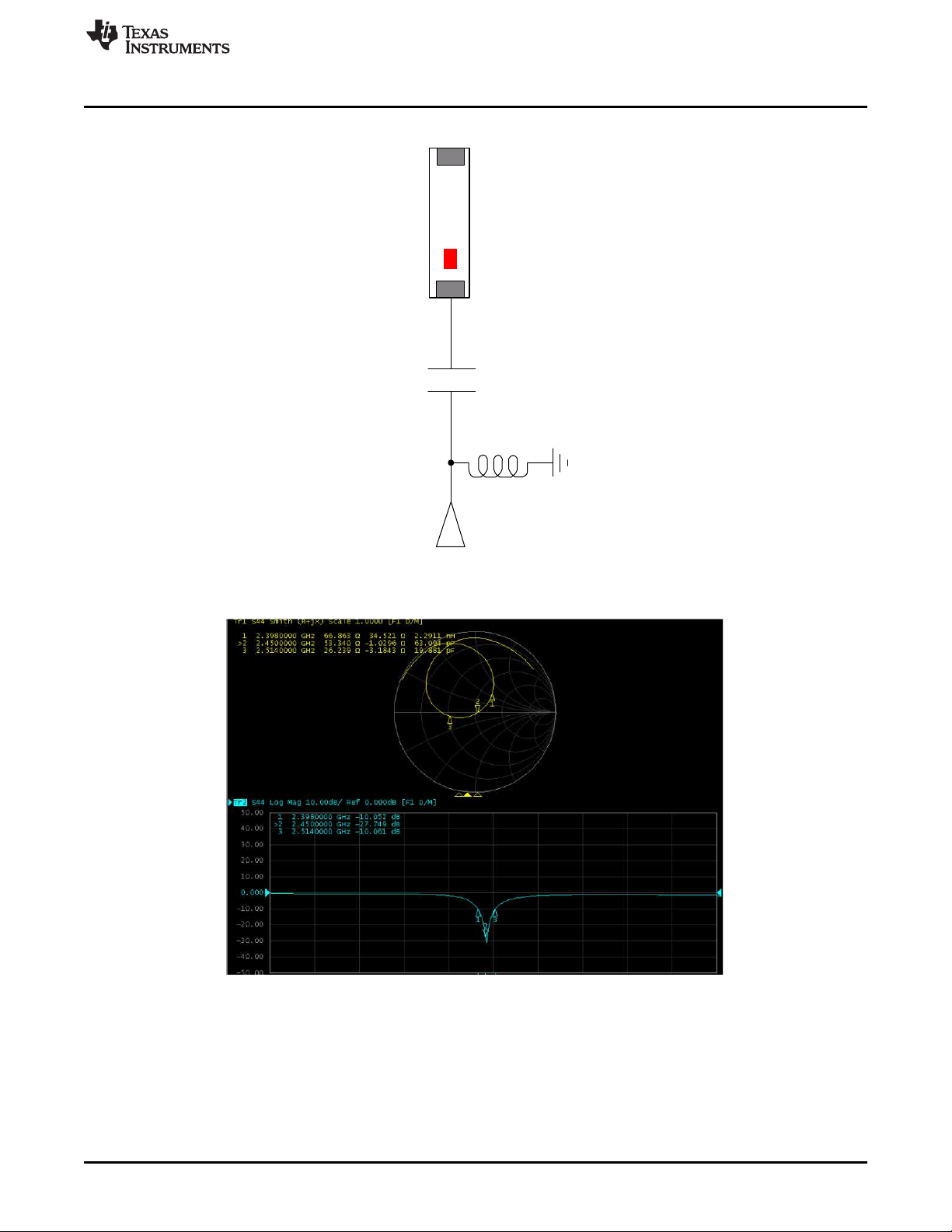
2.3 Antenna
The ACX ceramic antenna is mounted on the EM board with a specific layout and matching circuit for the
radiation tests conducted in FCC, CE, and IC certifications. Figure 2-3 shows the location of the ACX
ceramic antenna on the EM board and the RF trace routing from the CC3000 module to the antenna.
Figure 2-4 shows the matching circuit between the antenna and the EM board. The return loss is based
on the matching circuit and RF trace routing, as shown in Figure 2-5. Figure 2-6 shows the radiation
patterns on XY, XZ, and YZ planes.
www.ti.com
10
Figure 2-3. Antenna Location and RF Trace Routing
CC3000 EM Board SWRU326–November 2012
Copyright © 2012, Texas Instruments Incorporated
Submit Documentation Feedback
SWRU326-005
AT8010-E2R9HAA
2.2 pF
2.2 nH
SWRU326-004
www.ti.com
Antenna
Figure 2-4. Matching Circuit Between the Antenna and the CC3000 EM Board
Figure 2-5. Return Loss from the ACX Antenna and Matching Circuit
SWRU326–November 2012 CC3000 EM Board
Submit Documentation Feedback
Copyright © 2012, Texas Instruments Incorporated
11

SWRU326-006
YZ plane
XY plane
XZ plane
Unit : dBi
XY plane
Peak gain Avg. gain
0.3 –2.6
XZ plane
Peak gain Avg. gain
1.3 –4.2
YZ plane
Peak gain
Avg. gain
0.9 –0.9
Antenna
www.ti.com
Figure 2-6. Antenna Radiation Patterns
12
CC3000 EM Board SWRU326–November 2012
Copyright © 2012, Texas Instruments Incorporated
Submit Documentation Feedback

1.2 inches
J2
J1
20 19
1
2
20 19
1
2
SWRU326-007
www.ti.com
2.4 Hardware Setup
Before conducting performance tests, the EM board must be connected to the host platform, either with
the mating connectors (J6 and J7) or the single-row headers (J4 and J5). To use the EM mating
connectors to connect the hardware, the mating EM connector must be lined up and spaced 1.2 inches
apart (see Figure 2-7). To use the single-row headers, the required signals from the EM mating
connectors must be wired to the host platform.
Hardware Setup
Figure 2-7. Host PCB Mating Connector Arrangement
SWRU326–November 2012 CC3000 EM Board
Submit Documentation Feedback
Copyright © 2012, Texas Instruments Incorporated
13

SWRU326-008
Schematics
2.5 Schematics
Figure 2-8 shows the schematics of the CC3000 EM board.
www.ti.com
14
Figure 2-8. Schematics of the CC3000 EM Board
CC3000 EM Board SWRU326–November 2012
Copyright © 2012, Texas Instruments Incorporated
Submit Documentation Feedback
www.ti.com
2.6 Bill of Materials (BOM)
Table 2-7 lists the BOM for the TI CC3000 EM board.
Items Reference Designator Description
1 U1 TI CC3000 Wi-Fi b/g module (BM)
2 ANT1 ANT, 2.4 GHz, peak gain 2.5 dB
3 J1 Mini RF header receptacle
4 J2 CON male 1 x 3, pitch 2.0 mm
5 J3 CON male 1 x 2, pitch 2.0 mm
6 J6,J7 Female header, Fool Proof H:4.3, 2 x 10, pitch 1.27 mm, SMT
7 C1,C3 CAP 0402 10 pF, 50 V, NPO, ±5%
8 C4,C5 CAP 0402 1 µF, X5R, 6.3 V, ±10%, HF
9 R1, R2, R3, R4, R5, R6, R8, R9, R10, RES 0402, 0-Ω jumper
R11, R13, R15, R16, R17, R18, R19, R20,
10 R14 RES 0603, 0-Ω jumper
Bill of Materials (BOM)
Table 2-7. BOM for the TI CC3000 EM Board
R21
SWRU326–November 2012 CC3000 EM Board
Submit Documentation Feedback
Copyright © 2012, Texas Instruments Incorporated
15
SWRU326-014
Chapter 3
SWRU326–November 2012
Layout Guidelines
This section presents guidelines that must be followed when creating a board design incorporating the TI
CC3000 module.
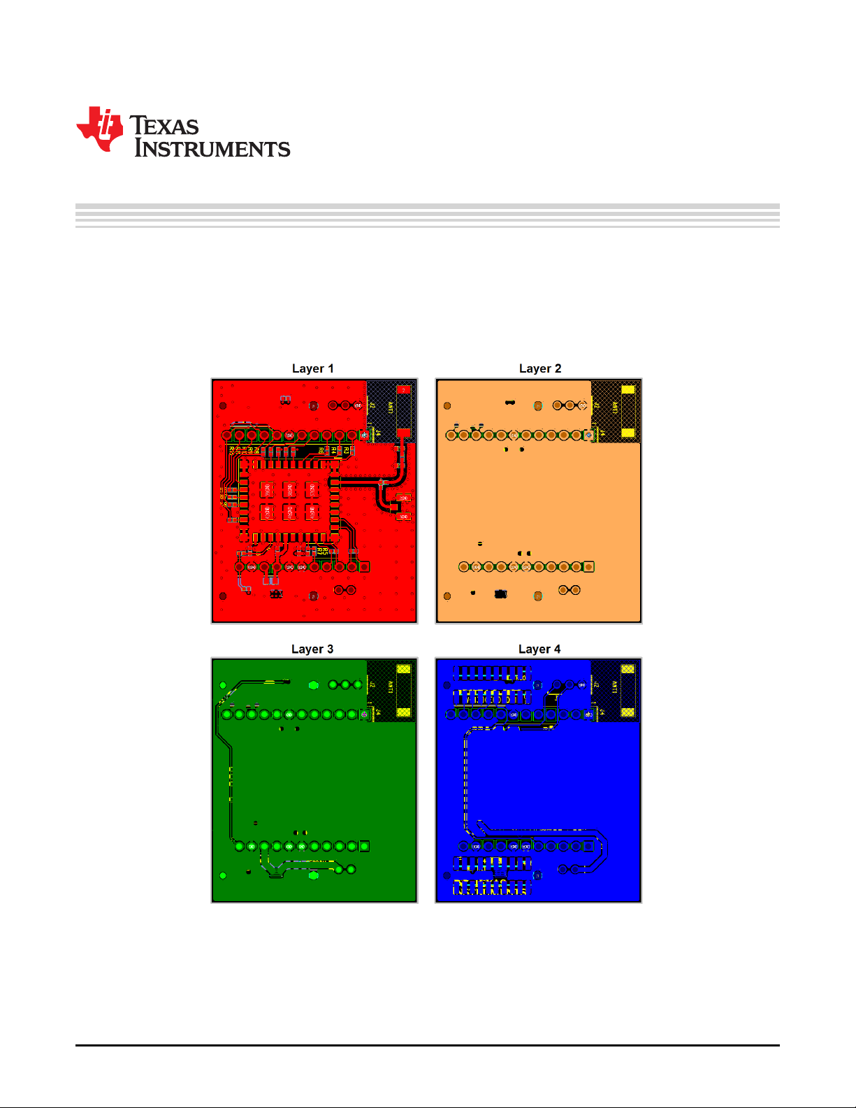
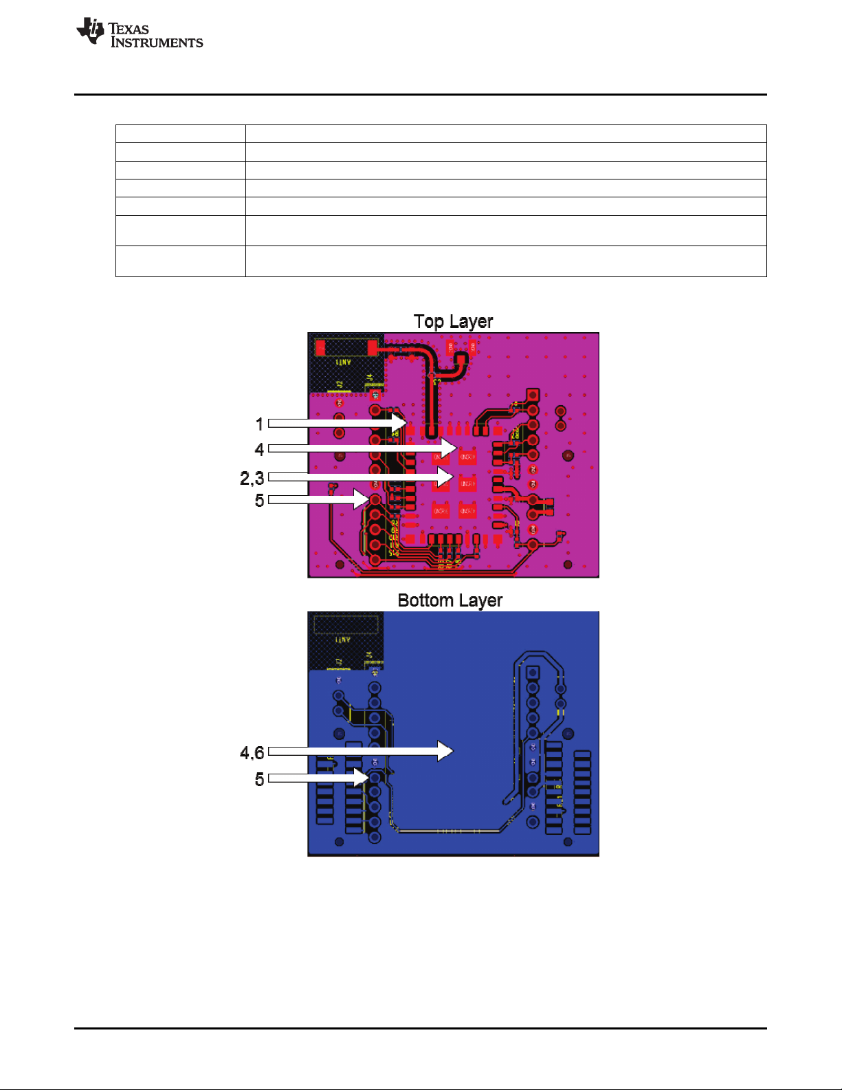
Figure 3-1 shows the TI CC3000 EM four-layer board. Table 3-1 and Figure 3-2 describe instances of
good layout practices.
16
Figure 3-1. Module Layout Guidelines
Layout Guidelines SWRU326–November 2012
Copyright © 2012, Texas Instruments Incorporated
Submit Documentation Feedback
SWRU326-013
www.ti.com
(1)
Reference
1 The proximity of ground vias must be close to the pad.
2 Signal traces must not be run underneath the module on the layer where the module is mounted.
3 Have a complete ground pour in layer 2 for thermal dissipation.
4 Have a solid ground plane and ground vias under the module for stable system and thermal dissipation.
5 Increase the ground pour in the first layer and have all of the traces from the first layer on the inner
6 Signal traces can be run on a third layer under the solid ground layer, which is below the module
See Figure 3-2.
Table 3-1. Module Layout Guidelines
(1)
layers, if possible.
mounting layer.
Guideline Description
Figure 3-2. Module Layout Guidelines
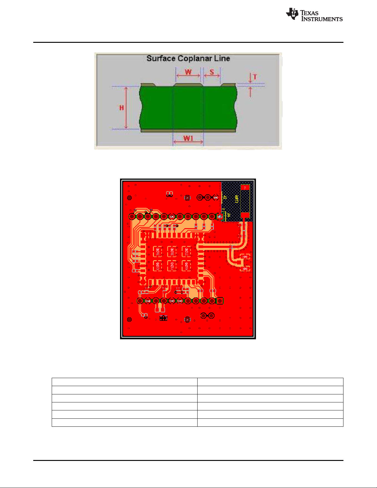
Figure 3-3 shows the trace design for the PCB. A 50-Ω impedance match on the trace to the antenna
should be used. Also, 50-Ω traces are recommended for the PCB layout. Table 3-2 lists the distances
shown in Figure 3-3. Figure 3-4 shows layer 1 with the trace to the antenna over ground layer 2. Table 3-3
and Figure 3-5 describe instances of good layout practices for the antenna and RF trace routing.
SWRU326–November 2012 Layout Guidelines
Submit Documentation Feedback
Copyright © 2012, Texas Instruments Incorporated
17
SWRU326-015
SWRU326-010
Figure 3-3. Trace Design for the PCB Layout
www.ti.com
Figure 3-4. Layer 1 Combined With Layer 2
Table 3-2. Trace Design Measurement Values
Measurement Length
H (height between L1 and L2) 12.0 mil
W (RF trace) 14.3 mil
T (thickness) 1.2 mil
S (separation) 10.0 mil
ε
(dielectric) 4.3
r
18
Layout Guidelines SWRU326–November 2012
Copyright © 2012, Texas Instruments Incorporated
Submit Documentation Feedback

SWRU326-011
www.ti.com
(1)
Reference
1 The RF trace antenna feed must be as short as possible beyond the ground reference. At this point, the
2 The RF trace bends must be gradual with an approximate maximum bend of 45 degrees with trace
3 RF traces must have via stitching on the ground plane beside the RF trace on both sides.
4 RF traces must have constant impedance (microstrip transmission line).
5 For best results, the RF trace ground layer must be the ground layer immediately below the RF trace.
6 There must be no traces or ground under the antenna section.
7 The PCB designer must understand the microstrip model used and the scale line width according to the
8 RF traces must be as short as possible. The antenna, RF traces, and modules must be on the edge of
See Figure 3-5.
Table 3-3. Antenna and RF Trace Routing Layout Guidelines
(1)
trace starts to radiate.
mitered. RF traces must not have sharp corners.
The ground layer must be solid.
microstrip model.
the PCB product. The proximity of the antenna to the enclosure and the enclosure material must also be
considered.
Guideline Description
Figure 3-5. Antenna and RF Trace Routing Layout Guidelines
SWRU326–November 2012 Layout Guidelines
Submit Documentation Feedback
Copyright © 2012, Texas Instruments Incorporated
19
SWRU326-012
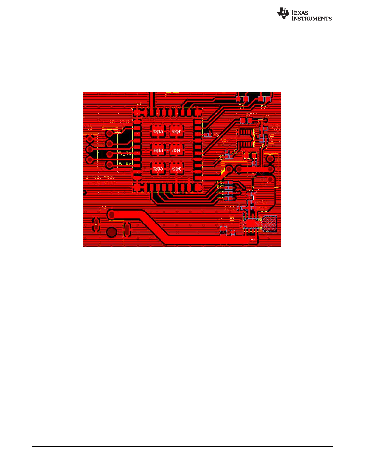
Figure 3-6 shows the supply routing guidelines:
• For power supply routing, the power trace for VBAT must be at least 40 mil wide.
• The 1.8-V trace must be at least 18 mil wide.
• Make VBAT traces as wide as possible to ensure reduced inductance and trace resistance.
• If possible, shield VBAT traces with ground above, below, and beside the traces.
www.ti.com
Figure 3-6. Power Supply Routing of the CC3000 EM Board
20
Layout Guidelines SWRU326–November 2012
Copyright © 2012, Texas Instruments Incorporated
Submit Documentation Feedback
Chapter 4
SWRU326–November 2012
Application Development
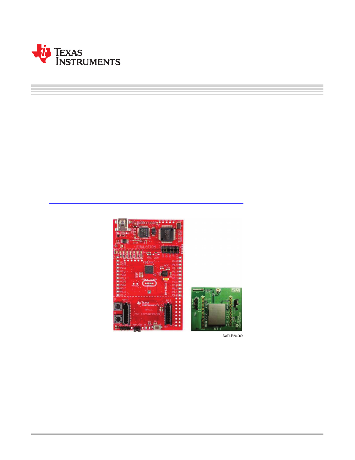
TI supports the CC3000 EM board when paired with the following TI MCU host platforms:
• MSP-EXP430FR5739
• MSP-EXP430F5529
• MSP-EXP430F5438
• MSP-EXP430FG4618
• DK-LM3S9B96
• EK-LM4F232
To find example applications for each of the listed host platforms, go to the TI wiki at:
http://processors.wiki.ti.com/index.php/CC3000_Wi-Fi_for_MCU#TI_Platforms.
In addition to the TI MCU platforms, the CC3000 EM board can be used on other platforms with the same
RF connector interface. For a host driver porting guide to assist with porting to other platforms, go to
http://processors.wiki.ti.com/index.php/CC3000_Host_Driver_Porting_Guide.
Figure 4-1 shows the MSP-EXP430FR5739 test platform and CC3000 EM board.
Figure 4-1. MSP-EXP430FR5739 Test Platform and CC3000 EM Board
SWRU326–November 2012 Application Development
Submit Documentation Feedback
Copyright © 2012, Texas Instruments Incorporated
21

IMPORTANT NOTICE
Texas Instruments Incorporated and its subsidiaries (TI) reserve the right to make corrections, enhancements, improvements and other
changes to its semiconductor products and services per JESD46, latest issue, and to discontinue any product or service per JESD48, latest
issue. Buyers should obtain the latest relevant information before placing orders and should verify that such information is current and
complete. All semiconductor products (also referred to herein as “components”) are sold subject to TI’s terms and conditions of sale
supplied at the time of order acknowledgment.
TI warrants performance of its components to the specifications applicable at the time of sale, in accordance with the warranty in TI’s terms
and conditions of sale of semiconductor products. Testing and other quality control techniques are used to the extent TI deems necessary
to support this warranty. Except where mandated by applicable law, testing of all parameters of each component is not necessarily
performed.
TI assumes no liability for applications assistance or the design of Buyers’ products. Buyers are responsible for their products and
applications using TI components. To minimize the risks associated with Buyers’ products and applications, Buyers should provide
adequate design and operating safeguards.
TI does not warrant or represent that any license, either express or implied, is granted under any patent right, copyright, mask work right, or
other intellectual property right relating to any combination, machine, or process in which TI components or services are used. Information
published by TI regarding third-party products or services does not constitute a license to use such products or services or a warranty or
endorsement thereof. Use of such information may require a license from a third party under the patents or other intellectual property of the
third party, or a license from TI under the patents or other intellectual property of TI.
Reproduction of significant portions of TI information in TI data books or data sheets is permissible only if reproduction is without alteration
and is accompanied by all associated warranties, conditions, limitations, and notices. TI is not responsible or liable for such altered
documentation. Information of third parties may be subject to additional restrictions.
Resale of TI components or services with statements different from or beyond the parameters stated by TI for that component or service
voids all express and any implied warranties for the associated TI component or service and is an unfair and deceptive business practice.
TI is not responsible or liable for any such statements.
Buyer acknowledges and agrees that it is solely responsible for compliance with all legal, regulatory and safety-related requirements
concerning its products, and any use of TI components in its applications, notwithstanding any applications-related information or support
that may be provided by TI. Buyer represents and agrees that it has all the necessary expertise to create and implement safeguards which
anticipate dangerous consequences of failures, monitor failures and their consequences, lessen the likelihood of failures that might cause
harm and take appropriate remedial actions. Buyer will fully indemnify TI and its representatives against any damages arising out of the use
of any TI components in safety-critical applications.
In some cases, TI components may be promoted specifically to facilitate safety-related applications. With such components, TI’s goal is to
help enable customers to design and create their own end-product solutions that meet applicable functional safety standards and
requirements. Nonetheless, such components are subject to these terms.
No TI components are authorized for use in FDA Class III (or similar life-critical medical equipment) unless authorized officers of the parties
have executed a special agreement specifically governing such use.
Only those TI components which TI has specifically designated as military grade or “enhanced plastic” are designed and intended for use in
military/aerospace applications or environments. Buyer acknowledges and agrees that any military or aerospace use of TI components
which have not been so designated is solely at the Buyer's risk, and that Buyer is solely responsible for compliance with all legal and
regulatory requirements in connection with such use.
TI has specifically designated certain components which meet ISO/TS16949 requirements, mainly for automotive use. Components which
have not been so designated are neither designed nor intended for automotive use; and TI will not be responsible for any failure of such
components to meet such requirements.
Products Applications
Audio www.ti.com/audio Automotive and Transportation www.ti.com/automotive
Amplifiers amplifier.ti.com Communications and Telecom www.ti.com/communications
Data Converters dataconverter.ti.com Computers and Peripherals www.ti.com/computers
DLP® Products www.dlp.com Consumer Electronics www.ti.com/consumer-apps
DSP dsp.ti.com Energy and Lighting www.ti.com/energy
Clocks and Timers www.ti.com/clocks Industrial www.ti.com/industrial
Interface interface.ti.com Medical www.ti.com/medical
Logic logic.ti.com Security www.ti.com/security
Power Mgmt power.ti.com Space, Avionics and Defense www.ti.com/space-avionics-defense
Microcontrollers microcontroller.ti.com Video and Imaging www.ti.com/video
RFID www.ti-rfid.com
OMAP Applications Processors www.ti.com/omap TI E2E Community e2e.ti.com
Wireless Connectivity www.ti.com/wirelessconnectivity
Mailing Address: Texas Instruments, Post Office Box 655303, Dallas, Texas 75265
Copyright © 2012, Texas Instruments Incorporated

REGULATORY COMPLIANCE INFORMATION
When the radio module is included in a final product, the following warning statements must be included in the final
product user guide
Caution
This device complies with part 15 of the FCC Rules. Operation is subject to the following two conditions: (1) This device may not
cause harmful interference, and (2) this device must accept any interference received, including interference that may cause
undesired operation.
Changes or modifications not expressly approved by the party responsible for compliance could void the user's authority to operate
the equipment.
FCC Interference Statement for Class A devices
This equipment has been tested and found to comply with the limits for a Class A digital device, pursuant to part 15 of the FCC
Rules. These limits are designed to provide reasonable protection against harmful interference when the equipment is operated in a
commercial environment. This equipment generates, uses, and can radiate radio frequency energy and, if not installed and used in
accordance with the instruction manual, may cause harmful interference to radio communications. Operation of this equipment in a
residential area is likely to cause harmful interference in which case the user will be required to correct the interference at his own
expense.
FCC Interference Statement for Class B devices
This equipment has been tested and found to comply with the limits for a Class B digital device, pursuant to part 15 of the FCC
Rules. These limits are designed to provide reasonable protection against harmful interference in a residential installation. This
equipment generates, uses and can radiate radio frequency energy and, if not installed and used in accordance with the
instructions, may cause harmful interference to radio communications. However, there is no guarantee that interference will not
occur in a particular installation. If this equipment does cause harmful interference to radio or television reception, which can be
determined by turning the equipment off and on, the user is encouraged to try to correct the interference by one or more of the
following measures:
• Reorient or relocate the receiving antenna.
• Increase the separation between the equipment and receiver.
• Connect the equipment into an outlet on a circuit different from that to which the receiver is connected.
• Consult the dealer or an experienced radio/TV technician for help.
Industry Canada Warnings
This Class B digital apparatus complies with Canadian ICES-003.
Changes or modifications not expressly approved by the party responsible for compliance could void the user’s authority to operate
the equipment.
This device complies with Industry Canada licence-exempt RSS standard(s). Operation is subject to the following two conditions: (1)
this device may not cause interference, and (2) this device must accept any interference, including interference that may cause
undesired operation of the device.
Under Industry Canada regulations, this radio transmitter may only operate using an antenna of a type and maximum (or lesser)
gain approved for the transmitter by Industry Canada. To reduce potential radio interference to other u sers, the antenna type and its
gain should be so chosen that the equivalent isotropically radiated power (e.i.r.p.) is not more than that necessary for successful
communication. This radio transmitter has been approved by Industry Canada to operate with the antenna types listed in the user
guide with the maximum permissible gain and required antenna impedance for each antenna type indicated. Antenna types not
included in this list, having a gain greater than the maximum gain indicated for that type, are strictly prohibited for use with this
device.
Cet appareil numérique de la classe A ou B est conforme à la norme NMB-003 du Canada.
Les changements ou les modifications pas expressément approuvés par la partie responsable de la conformité ont pu vider
l’autorité de l'utilisateur pour actionner l'équipement.
Le présent appareil est conforme aux CNR d'Industrie Canada applicables aux appareils radio exempts de licence. L'exploitation
autorisée aux deux conditions suivantes : (1) l'appareil ne doit pas produire de brouillage, et (2) l'utilisateur de l'appareil doit
accepter tout brouillage radioélectrique subi, même si le brouillage est susceptible d'en compromettre le fonctionnement.
Conformément à la réglementation d'Industrie Canada, le présent émetteur radio peut fonctionner avec une antenne d'un type et
d'un gain maximal (ou inférieur) approuvé pour l'émetteur par Industrie Canada. Dans le but de réduire les risques de brouillage
radioélectrique à l'intention des autres utilisateurs, il faut choisir le type d'antenne et son gain de sorte que la puissance isotrope
rayonnée équivalente (p.i.r.e.) ne dépasse pas l'intensité nécessaire à l'établissement d'une communication satisfaisante.
Le présent émetteur radio a été approuvé par Industrie Canada pour fonctionner avec les types d'antenne énumérés dans le
manuel d’usage et ayant un gain admissible maximal et l'impédance requise pour chaque type d'antenne. Les types d'antenne non
inclus dans cette liste, ou dont le gain est supérieur au gain maximal indiqué, sont strictement interdits pour l'exploitation de
l'émetteur.
Labeling of the final product
The final product must contain a label with the statement “Contains radio module FCC ID: Z64-CC3000EM, IC: 451I-CC3000EM”.
est
 Loading...