

Page 1
CC256x QFN EM User Guide
CC256x QFN EM User Guide
This User Guide is intended for use with TI's Bluetooth development platform, the CC256x QFN EM board. This
guide will help you quickly get started with this board to integrate with TI's evaluation platforms and software
SDK's. In addition, this user guide describes the components/configurations of this board to quickly get started with
using this board for various Bluetooth applications.
Introduction to CC256x QFN EM Board
This guide will provide information about the module so you can utilize the board specifics to apply it to your
application. Module information and capabilities including pin descriptions and available software and tools will
enhance your out of box experience.
1
Key Features
• Bluetooth Specification v4.0
• Fast Time to Market
• Easy PCB Layout Using Cadence Tools
• 4 Layer PCB design
• Bluetooth & Bluetooth Low Energy or ANT
• StoneStreet One Bluetopia Stack with many profiles
• Other Profiles Available on Request i.e. Audio Profiles
• FCC, IC, BT SIG Compliant
• High sensitivity (-93 dBm typ.)
• Shield enabled for immunity
• H4 UART and PCM/I2S Interface
Page 2
CC256x QFN EM User Guide
QFN EM Board Applications
Example Embedded Wireless Applications:
• Cable Replacement
• Printer Adapters
• Personal Digital Assistants (PDAs)
• Printers/Scanners
• Computers and Peripherals
• Wireless Sensors
• Industrial Control Applications
• Low Power Medical
Module Description
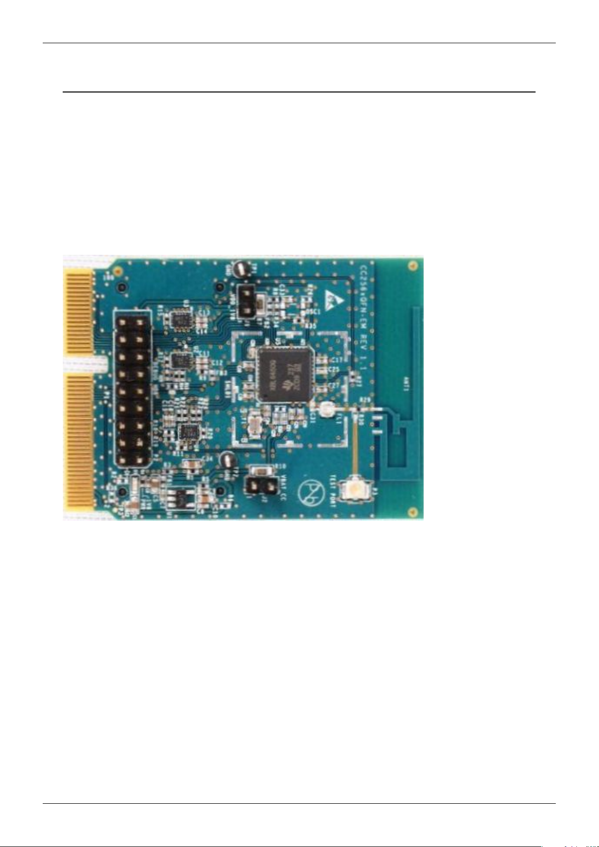
The CC256x QFN EM board is the development environment for the CC256x family and plugs directly into Texas
Instruments MSP430 and Stellaris experimenter boards with the added benefit of header connectors that simplify
prototype wiring and field trials.
This family is based upon Texas Instrument’s CC256x integrated circuits and uses a Host Controller Interface (HCI),
a cost effective and flexible means to implement a Bluetooth network. HCI reduces BOM cost by eliminating
redundant processing capacity and giving designers the flexibility to work with a controller of their choosing, as the
Bluetooth stack resides and executes on the application
’s host processor.
2
The CC256x QFN EM board is intended for evaluation purpose and works with Texas Instrument’s Hardware
Development Kit. Please refer to
To aid in the implementation of this reference design, schematic and layout files are available on the CC256x Main
Wiki page.
Tools and Software Section.
Page 3
CC256x QFN EM User Guide
Module Detailed Description
The reference files including schematic, layout, and BOM for the CC256x QFN EM board can be found at the
following link:
CC256x QFN EM v1.2 Reference Design (swrr117)
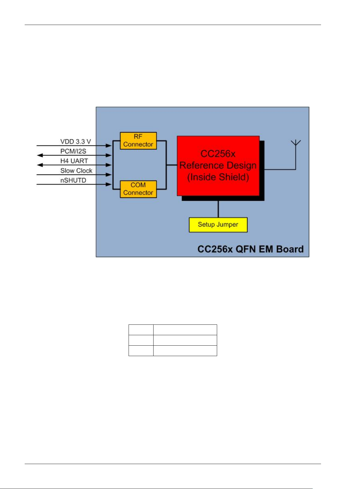
Below is a block diagram depicting the input/outputs of the QFN board that is required for interfacing to host
controller. These I/O's can be interfaced to the host controller either through the COM connector or the RF1 & RF2
sockets.
[1]
3
Pin Description
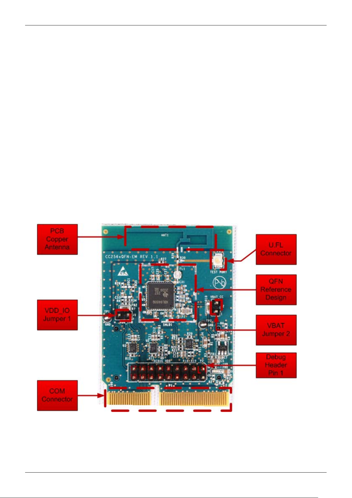
Board Jumpers
For correct operation, please make sure both jumpers are placed for connecting power to the device:
Jumper Configuration
Jumper Description
VBAT_CC Main power supply for CC256x
VDD_1V8 Supplies power to CC256x I/O's
Page 4
CC256x QFN EM User Guide
Measuring Current Consumption
These jumpers can also be used to measure the current consumption by placing current sense resistors on R10 for
VBAT_CC and R7 for VDD_1V8. Both these resistors are 0.10 Ohm, 1/4 W. VBAT_CC jumper can be used to to
measure the voltage/power consumed by the CC256x including RF TX/RX while VDD_IO jumper can be used to
measure voltage/power consumed by the digital I/O's.
Antenna/U.FL Selector
The board can be configured to route the RF output from the CC256x to the on board copper antenna or the on board
U.FL connector. This configuration is done by placing the resistor in either R29 or R30 position which has negligible
resistance of a 0 Ohm. R30 will connect the RF to the U.FL while R29 will connect to the copper antenna. The U.FL
connector is used for conducted testing of the RF. The Bluetooth Hardware Evaluation Tool (BHET)
[2]
to test basic RF functionality on this board.
RF Connectors
The RF1 and RF2 connectors can be used to mount on a wide variety of TI MCU platforms such as MSP430 and
Stellaris. Note that the RF I/O's are all at 3.3V levels. This enables seamless integration of the host using TI's
platforms that comes preinstalled with EM headers. The standard pinout is described in the following table:
4
can be used
RF1
Pin # EM Adapter Pin Assignment Pin # EM Adapter Pin Assignment
1 GND 2 N/C
3 MODULE_UART_CTS 4 N/C
5 SLOW_CLK 6 N/C
7 MODULE_UART_RX 8 N/C
9 MODULE_UART_TX 10 N/C
11 N/C 12 N/C
13 N/C 14 N/C
15 N/C 16 N/C
17 N/C 18 N/C
19 GND 20 N/C
RF2
Pin # EM Adapter Pin Assignment Pin # EM Adapter Pin Assignment
1 N/C 2 GND
3 N/C 4 N/C
5 N/C 6 N/C
7 +3.3V 8 MODULE_AUDIO_DATA_OUT
9 +3.3V 10 MODULE_AUDIO_DATA_IN
11 MODULE_AUDIO_FSYNC 12 N/C
13 N/C 14 N/C
15 N/C 16 N/C
Page 5

CC256x QFN EM User Guide
17 MODULE_AUDIO_CLK 18 MODULE_UART_RTS
19 WCS_NSHUTD 20 N/C
Debug Header
The debug header is provided for testing and debugging purposes. It exposes important signals used in the design
such as power, ground, debug, UART, and Audio signals. Note that all I/O's are at 1.8V. Pinout is shown in the
following table:
DEBUG HDR
Pin # EM Adapter Pin Assignment Pin€# EM Adapter Pin Assignment
1 GND 2 VBAT
3 VIO_HOST 4 GND
5 AUD_FSYNC_1V8 6 AUD_CLK_1V8
7 AUD_OUT_1V8 8 AUD_IN_1V8
9 CLK_REQ_OUT_1V8 10 SLOW_CLK_EDGE
5
11 HCI_TX_1V8 12 HCI_RX_1V8
13 HCI_CTS_1V8 14 HCI_RTS_1V8
15 TX_DEBUG_1V8 16 nSHUTDOWN_1V8
17 VDD_1V8 18 GND
COM Connector
The COM connector, aka Edge card, is used to interface with TI's MPUs such as OMAP and AM335x. As shown
below, it provides HCI, Audio, Slow Clock, Shutdown, and Debug interfaces to the host connected through the edge
card. Note that all I/O's for the COM connector are at 1.8V. Also note some components should be DNI to use the
COM connector. See BOM for details.
COM€CARD
Pin # Relevant COM Connector Pin Assignment
1 SLOW_CLK_EDGE
8 1V8_IN
52 AUD_CLK_1V8
54 AUD_FSYNC_1V8
56 AUD_IN_1V8
58 AUD_OUT_1V8
66 HCI_TX_1V8
68 HCI_RX_1V8
70 HCI_CTS_1V8
72 HCI_RTS_1V8
76 TX_DEBUG_1V8
89 nSHUTDOWN_1V8
Page 6

CC256x QFN EM User Guide
Pins 3, 9, 19, 37, 47, 63, 77, 83, 87, 95, 97, and 2, 6, 18, 22, 42, 60, 64, 92 are connected to ground.
All other pins are NC (Not Connected).
Clock Inputs
• The slow clock can come from 2 sources, internal and external to the board. The CC256x QFN EM gives option
to place the slow clock on the board itself or source it from an external source. It is connected to the
SLOW_CLK_IN and can be a digital signal in the range of 0-1.8 V.
• The slow clock's frequency accuracy must be 32.768 kHz, 250 ppm for Bluetooth usage (according to the
Bluetooth specification).
• When the MSP430 Experimenter board is connected, the signal is exposed from the µController. So within this
application there is no additional clock needed.
6
Module Dimensions
No. Item Dimension [in] Tolerance Remark
1 Width 1.550 +/- 0.001 Smaller at COM end
2 Length 2.125 +/- 0.001
3 Height 0.062 +/- 0.001
Page 7

CC256x QFN EM User Guide
Tools and Software
Bluetopia Software Solution
Stone Street One has developed Bluetooth software based on their Bluetopia stack, including a few profiles, for
many platforms including TI
Demo APPS page.
[3]
Evaluation Platforms
These are the evaluation platforms we support:
• MSP430F5438 Experimenter's Board
• Stellaris LM3S9D96 kit
• Stellaris LM4F232 kit
• MSP430F5529 Experimenter's Board
In addition, a software development environment, e.g. Code Composer Studio, is required.
For a detailed description on usage of these tools please refer to: CC256x EVM Platform
Evaluation kits and modules are available through TI's network of authorized distributors.
’s MSP430 and Stellaris platforms. Detailed documentation is available in the Bluetooth
[4]
[5]
7
Below is a picture of the CC256x QFN EM board mounted to one of the platforms, the MSP430F5438
Experimenter's Board, using RF1 and RF2 interface:
Bluetooth Hardware Evaluation Tool
The CC256x Bluetooth Hardware Evaluation Tool
from Texas Instruments. It is a very intuitive, user-friendly tool to test TI's Bluetooth chips including this CC256x
QFN EM board. More specifically, it is used to measure RF performance of our BT chips.
[2]
is a program which can be downloaded as a complete package
Certification
The CC256x QFN EM board is currently undergoing FCC, CI, and ETSI certification. It is also in process of being
certified as a Bluetooth controller subsystem by the Bluetooth SIG(Special Interest Group).
Life Support Policy
This TI product is not designed for use in life support appliances, devices, or systems where malfunction can
reasonably be expected to result in a significant personal injury to the user, or as a critical component in any life
support device or system whose failure to perform can be reasonably expected to cause the failure of the life support
device or system, or to affect its safety or effectiveness. TI customers using or selling these products for use in such
applications do so at their own risk and agree to fully indemnify TI for any damages resulting.
Page 8

CC256x QFN EM User Guide
Related Documents
• CC256x QFN Data Manual (swrs121a)
• CC256x System Design Guide
• [Coming Soon: CC256x PCB design checklist]
References
[7]
8
[6]
[1] http:/
[2] http:/ / processors. wiki. ti. com/ index. php/ CC256x_Bluetooth_Hardware_Evaluation_Tool
[3] http:/ / processors. wiki. ti. com/ index. php/ CC256x_MSP430_Bluetopia_Basic_Demo_APPS
[4] http:/ / processors. wiki. ti. com/ index. php/ CC256X_MSP:EXP430F5438
[5] http:/ / processors. wiki. ti. com/ index. php/ CC256x_EVM_Platform
[6] http:/ / www. ti. com/ litv/ pdf/ swrs121a
[7] http:/ / processors. wiki. ti. com/ index. php/ CC256x_System_Design_Guide
/ www. ti. com/ litv/ zip/ swrr117
Page 9

Article Sources and Contributors
Article Sources and Contributors
CC256x QFN EM User Guide ‚Source: http://processors.wiki.ti.com/index.php?oldid=136180 ‚Contributors: Nfatemi, Raisa, Zhaq
Image Sources, Licenses and Contributors
Image:CC256x QFN EM2.JPG ‚Source: http://processors.wiki.ti.com/index.php?title=File:CC256x_QFN_EM2.JPG ‚License: unknown ‚Contributors: Nfatemi
Image:CC256x QFN description.png ‚Source: http://processors.wiki.ti.com/index.php?title=File:CC256x_QFN_description.png ‚License: unknown ‚Contributors: Zhaq
Image:CC256x QFNDiagram.jpg ‚Source: http://processors.wiki.ti.com/index.php?title=File:CC256x_QFNDiagram.jpg ‚License: unknown ‚Contributors: Zhaq
Image:CC256x QFN slowCLK.png ‚Source: http://processors.wiki.ti.com/index.php?title=File:CC256x_QFN_slowCLK.png ‚License: unknown ‚Contributors: Zhaq
License
THE WORK (AS DEFINED BELOW) IS PROVIDED UNDER THE TERMS OF THIS CREATIVE COMMONS PUBLIC LICENSE ("CCPL" OR "LICENSE"). THE WORK IS PROTECTED BY COPYRIGHT AND/OR OTHER
APPLICABLE LAW. ANY USE OF THE WORK OTHER THAN AS AUTHORIZED UNDER THIS LICENSE OR COPYRIGHT LAW IS PROHIBITED.
BY EXERCISING ANY RIGHTS TO THE WORK PROVIDED HERE, YOU ACCEPT AND AGREE TO BE BOUND BY THE TERMS OF THIS LICENSE. TO THE EXTENT THIS LICENSE MAY BE CONSIDERED TO BE
A CONTRACT, THE LICENSOR GRANTS YOU THE RIGHTS CONTAINED HERE IN CONSIDERATION OF YOUR ACCEPTANCE OF SUCH TERMS AND CONDITIONS.
License
1. Definitions
a. "Adaptation" means a work based upon the Work, or upon the Work and other pre-existing works, such as a translation, adaptation, derivative work, arrangement of music or other alterations of a literary or artistic work, or
phonogram or performance and includes cinematographic adaptations or any other form in which the Work may be recast, transformed, or adapted including in any form recognizably derived from the original, except that a work
that constitutes a Collection will not be considered an Adaptation for the purpose of this License. For the avoidance of doubt, where the Work is a musical work, performance or phonogram, the synchronization of the Work in
timed-relation with a moving image ("synching") will be considered an Adaptation for the purpose of this License.
b. "Collection" means a collection of literary or artistic works, such as encyclopedias and anthologies, or performances, phonograms or broadcasts, or other works or subject matter other than works listed in Section 1(f) below,
which, by reason of the selection and arrangement of their contents, constitute intellectual creations, in which the Work is included in its entirety in unmodified form along with one or more other contributions, each constituting
separate and independent works in themselves, which together are assembled into a collective whole. A work that constitutes a Collection will not be considered an Adaptation (as defined below) for the purposes of this License.
c. "Creative Commons Compatible License" means a license that is listed at http:/ / creativecommons. org/ compatiblelicenses that has been approved by Creative Commons as being essentially equivalent to this License,
including, at a minimum, because that license: (i) contains terms that have the same purpose, meaning and effect as the License Elements of this License; and, (ii) explicitly permits the relicensing of adaptations of works made
available under that license under this License or a Creative Commons jurisdiction license with the same License Elements as this License.
d. "Distribute" means to make available to the public the original and copies of the Work or Adaptation, as appropriate, through sale or other transfer of ownership.
e. "License Elements" means the following high-level license attributes as selected by Licensor and indicated in the title of this License: Attribution, ShareAlike.
f. "Licensor" means the individual, individuals, entity or entities that offer(s) the Work under the terms of this License.
g. "Original Author" means, in the case of a literary or artistic work, the individual, individuals, entity or entities who created the Work or if no individual or entity can be identified, the publisher; and in addition (i) in the case of a
performance the actors, singers, musicians, dancers, and other persons who act, sing, deliver, declaim, play in, interpret or otherwise perform literary or artistic works or expressions of folklore; (ii) in the case of a phonogram the
producer being the person or legal entity who first fixes the sounds of a performance or other sounds; and, (iii) in the case of broadcasts, the organization that transmits the broadcast.
h. "Work" means the literary and/or artistic work offered under the terms of this License including without limitation any production in the literary, scientific and artistic domain, whatever may be the mode or form of its expression
including digital form, such as a book, pamphlet and other writing; a lecture, address, sermon or other work of the same nature; a dramatic or dramatico-musical work; a choreographic work or entertainment in dumb show; a
musical composition with or without words; a cinematographic work to which are assimilated works expressed by a process analogous to cinematography; a work of drawing, painting, architecture, sculpture, engraving or
lithography; a photographic work to which are assimilated works expressed by a process analogous to photography; a work of applied art; an illustration, map, plan, sketch or three-dimensional work relative to geography,
topography, architecture or science; a performance; a broadcast; a phonogram; a compilation of data to the extent it is protected as a copyrightable work; or a work performed by a variety or circus performer to the extent it is not
otherwise considered a literary or artistic work.
i. "You" means an individual or entity exercising rights under this License who has not previously violated the terms of this License with respect to the Work, or who has received express permission from the Licensor to exercise
rights under this License despite a previous violation.
j. "Publicly Perform" means to perform public recitations of the Work and to communicate to the public those public recitations, by any means or process, including by wire or wireless means or public digital performances; to
make available to the public Works in such a way that members of the public may access these Works from a place and at a place individually chosen by them; to perform the Work to the public by any means or process and the
communication to the public of the performances of the Work, including by public digital performance; to broadcast and rebroadcast the Work by any means including signs, sounds or images.
k. "Reproduce" means to make copies of the Work by any means including without limitation by sound or visual recordings and the right of fixation and reproducing fixations of the Work, including storage of a protected
performance or phonogram in digital form or other electronic medium.
2. Fair Dealing Rights
Nothing in this License is intended to reduce, limit, or restrict any uses free from copyright or rights arising from limitations or exceptions that are provided for in connection with the copyright protection under copyright law or other
applicable laws.
3. License Grant
Subject to the terms and conditions of this License, Licensor hereby grants You a worldwide, royalty-free, non-exclusive, perpetual (for the duration of the applicable copyright) license to exercise the rights in the Work as stated
below:
a. to Reproduce the Work, to incorporate the Work into one or more Collections, and to Reproduce the Work as incorporated in the Collections;
b. to create and Reproduce Adaptations provided that any such Adaptation, including any translation in any medium, takes reasonable steps to clearly label, demarcate or otherwise identify that changes were made to the original
Work. For example, a translation could be marked "The original work was translated from English to Spanish," or a modification could indicate "The original work has been modified.";
c. to Distribute and Publicly Perform the Work including as incorporated in Collections; and,
d. to Distribute and Publicly Perform Adaptations.
e. For the avoidance of doubt:
i. Non-waivable Compulsory License Schemes. In those jurisdictions in which the right to collect royalties through any statutory or compulsory licensing scheme cannot be waived, the Licensor reserves the exclusive right
to collect such royalties for any exercise by You of the rights granted under this License;
ii. Waivable Compulsory License Schemes. In those jurisdictions in which the right to collect royalties through any statutory or compulsory licensing scheme can be waived, the Licensor waives the exclusive right to collect
such royalties for any exercise by You of the rights granted under this License; and,
iii. Voluntary License Schemes. The Licensor waives the right to collect royalties, whether individually or, in the event that the Licensor is a member of a collecting society that administers voluntary licensing schemes, via
that society, from any exercise by You of the rights granted under this License.
The above rights may be exercised in all media and formats whether now known or hereafter devised. The above rights include the right to make such modifications as are technically necessary to exercise the rights in other media and
formats. Subject to Section 8(f), all rights not expressly granted by Licensor are hereby reserved.
4. Restrictions
The license granted in Section 3 above is expressly made subject to and limited by the following restrictions:
a. You may Distribute or Publicly Perform the Work only under the terms of this License. You must include a copy of, or the Uniform Resource Identifier (URI) for, this License with every copy of the Work You Distribute or
Publicly Perform. You may not offer or impose any terms on the Work that restrict the terms of this License or the ability of the recipient of the Work to exercise the rights granted to that recipient under the terms of the License.
You may not sublicense the Work. You must keep intact all notices that refer to this License and to the disclaimer of warranties with every copy of the Work You Distribute or Publicly Perform. When You Distribute or Publicly
Perform the Work, You may not impose any effective technological measures on the Work that restrict the ability of a recipient of the Work from You to exercise the rights granted to that recipient under the terms of the License.
This Section 4(a) applies to the Work as incorporated in a Collection, but this does not require the Collection apart from the Work itself to be made subject to the terms of this License. If You create a Collection, upon notice from
any Licensor You must, to the extent practicable, remove from the Collection any credit as required by Section 4(c), as requested. If You create an Adaptation, upon notice from any Licensor You must, to the extent practicable,
remove from the Adaptation any credit as required by Section 4(c), as requested.
b. You may Distribute or Publicly Perform an Adaptation only under the terms of: (i) this License; (ii) a later version of this License with the same License Elements as this License; (iii) a Creative Commons jurisdiction license
(either this or a later license version) that contains the same License Elements as this License (e.g., Attribution-ShareAlike 3.0 US)); (iv) a Creative Commons Compatible License. If you license the Adaptation under one of the
licenses mentioned in (iv), you must comply with the terms of that license. If you license the Adaptation under the terms of any of the licenses mentioned in (i), (ii) or (iii) (the "Applicable License"), you must comply with the
terms of the Applicable License generally and the following provisions: (I) You must include a copy of, or the URI for, the Applicable License with every copy of each Adaptation You Distribute or Publicly Perform; (II) You
may not offer or impose any terms on the Adaptation that restrict the terms of the Applicable License or the ability of the recipient of the Adaptation to exercise the rights granted to that recipient under the terms of the Applicable
License; (III) You must keep intact all notices that refer to the Applicable License and to the disclaimer of warranties with every copy of the Work as included in the Adaptation You Distribute or Publicly Perform; (IV) when
You Distribute or Publicly Perform the Adaptation, You may not impose any effective technological measures on the Adaptation that restrict the ability of a recipient of the Adaptation from You to exercise the rights granted to
that recipient under the terms of the Applicable License. This Section 4(b) applies to the Adaptation as incorporated in a Collection, but this does not require the Collection apart from the Adaptation itself to be made subject to
the terms of the Applicable License.
c. If You Distribute, or Publicly Perform the Work or any Adaptations or Collections, You must, unless a request has been made pursuant to Section 4(a), keep intact all copyright notices for the Work and provide, reasonable to the
medium or means You are utilizing: (i) the name of the Original Author (or pseudonym, if applicable) if supplied, and/or if the Original Author and/or Licensor designate another party or parties (e.g., a sponsor institute,
publishing entity, journal) for attribution ("Attribution Parties") in Licensor's copyright notice, terms of service or by other reasonable means, the name of such party or parties; (ii) the title of the Work if supplied; (iii) to the
extent reasonably practicable, the URI, if any, that Licensor specifies to be associated with the Work, unless such URI does not refer to the copyright notice or licensing information for the Work; and (iv) , consistent with
Ssection 3(b), in the case of an Adaptation, a credit identifying the use of the Work in the Adaptation (e.g., "French translation of the Work by Original Author," or "Screenplay based on original Work by Original Author"). The
credit required by this Section 4(c) may be implemented in any reasonable manner; provided, however, that in the case of a Adaptation or Collection, at a minimum such credit will appear, if a credit for all contributing authors of
the Adaptation or Collection appears, then as part of these credits and in a manner at least as prominent as the credits for the other contributing authors. For the avoidance of doubt, You may only use the credit required by this
Section for the purpose of attribution in the manner set out above and, by exercising Your rights under this License, You may not implicitly or explicitly assert or imply any connection with, sponsorship or endorsement by the
Original Author, Licensor and/or Attribution Parties, as appropriate, of You or Your use of the Work, without the separate, express prior written permission of the Original Author, Licensor and/or Attribution Parties.
d. Except as otherwise agreed in writing by the Licensor or as may be otherwise permitted by applicable law, if You Reproduce, Distribute or Publicly Perform the Work either by itself or as part of any Adaptations or Collections,
You must not distort, mutilate, modify or take other derogatory action in relation to the Work which would be prejudicial to the Original Author's honor or reputation. Licensor agrees that in those jurisdictions (e.g. Japan), in
which any exercise of the right granted in Section 3(b) of this License (the right to make Adaptations) would be deemed to be a distortion, mutilation, modification or other derogatory action prejudicial to the Original Author's
honor and reputation, the Licensor will waive or not assert, as appropriate, this Section, to the fullest extent permitted by the applicable national law, to enable You to reasonably exercise Your right under Section 3(b) of this
License (right to make Adaptations) but not otherwise.
5. Representations, Warranties and Disclaimer
UNLESS OTHERWISE MUTUALLY AGREED TO BY THE PARTIES IN WRITING, LICENSOR OFFERS THE WORK AS-IS AND MAKES NO REPRESENTATIONS OR WARRANTIES OF ANY KIND CONCERNING
THE WORK, EXPRESS, IMPLIED, STATUTORY OR OTHERWISE, INCLUDING, WITHOUT LIMITATION, WARRANTIES OF TITLE, MERCHANTIBILITY, FITNESS FOR A PARTICULAR PURPOSE,
NONINFRINGEMENT, OR THE ABSENCE OF LATENT OR OTHER DEFECTS, ACCURACY, OR THE PRESENCE OF ABSENCE OF ERRORS, WHETHER OR NOT DISCOVERABLE. SOME JURISDICTIONS DO NOT
ALLOW THE EXCLUSION OF IMPLIED WARRANTIES, SO SUCH EXCLUSION MAY NOT APPLY TO YOU.
6. Limitation on Liability
EXCEPT TO THE EXTENT REQUIRED BY APPLICABLE LAW, IN NO EVENT WILL LICENSOR BE LIABLE TO YOU ON ANY LEGAL THEORY FOR ANY SPECIAL, INCIDENTAL, CONSEQUENTIAL, PUNITIVE
OR EXEMPLARY DAMAGES ARISING OUT OF THIS LICENSE OR THE USE OF THE WORK, EVEN IF LICENSOR HAS BEEN ADVISED OF THE POSSIBILITY OF SUCH DAMAGES.
7. Termination
9
Page 10

License
a. This License and the rights granted hereunder will terminate automatically upon any breach by You of the terms of this License. Individuals or entities who have received Adaptations or Collections from You under this License,
however, will not have their licenses terminated provided such individuals or entities remain in full compliance with those licenses. Sections 1, 2, 5, 6, 7, and 8 will survive any termination of this License.
b. Subject to the above terms and conditions, the license granted here is perpetual (for the duration of the applicable copyright in the Work). Notwithstanding the above, Licensor reserves the right to release the Work under different
license terms or to stop distributing the Work at any time; provided, however that any such election will not serve to withdraw this License (or any other license that has been, or is required to be, granted under the terms of this
License), and this License will continue in full force and effect unless terminated as stated above.
8. Miscellaneous
a. Each time You Distribute or Publicly Perform the Work or a Collection, the Licensor offers to the recipient a license to the Work on the same terms and conditions as the license granted to You under this License.
b. Each time You Distribute or Publicly Perform an Adaptation, Licensor offers to the recipient a license to the original Work on the same terms and conditions as the license granted to You under this License.
c. If any provision of this License is invalid or unenforceable under applicable law, it shall not affect the validity or enforceability of the remainder of the terms of this License, and without further action by the parties to this
agreement, such provision shall be reformed to the minimum extent necessary to make such provision valid and enforceable.
d. No term or provision of this License shall be deemed waived and no breach consented to unless such waiver or consent shall be in writing and signed by the party to be charged with such waiver or consent.
e. This License constitutes the entire agreement between the parties with respect to the Work licensed here. There are no understandings, agreements or representations with respect to the Work not specified here. Licensor shall not
be bound by any additional provisions that may appear in any communication from You. This License may not be modified without the mutual written agreement of the Licensor and You.
f. The rights granted under, and the subject matter referenced, in this License were drafted utilizing the terminology of the Berne Convention for the Protection of Literary and Artistic Works (as amended on September 28, 1979),
the Rome Convention of 1961, the WIPO Copyright Treaty of 1996, the WIPO Performances and Phonograms Treaty of 1996 and the Universal Copyright Convention (as revised on July 24, 1971). These rights and subject
matter take effect in the relevant jurisdiction in which the License terms are sought to be enforced according to the corresponding provisions of the implementation of those treaty provisions in the applicable national law. If the
standard suite of rights granted under applicable copyright law includes additional rights not granted under this License, such additional rights are deemed to be included in the License; this License is not intended to restrict the
license of any rights under applicable law.
10
Page 11

Texas Instruments (TI) provides the enclosed Evaluation Board/Kit/Module (EVM) under the following
conditions:
The user assumes all responsibility and liability for proper and safe handling of the goods. Further, the user
indemnifies TI from all claims arising from the handling or use of the goods.
Should this evaluation board/kit not meet the specifications indicated in the User’s Guide, the board/ kit may
be returned within 30 days from the date of delivery for a full refund. THE FOREGOING LIMITED
WARRANTY IS THE EXCLUSIVE WARRANTY MADE BY SELLER TO BUYER AND IS IN LIEU OF ALL
OTHER WARRANTIES, EXPRESSED, IMPLIED, OR STATUTORY, INCLUDING ANY WARRANTY OF
MERCHANTABILITY OR FITNESS FOR ANY PARTICULAR PURPOSE. EXCEPT TO THE EXTENT OF
THE INDEMNITY SET FORTH ABOVE, NEITHER PARTY SHALL BE LIABLE TO THE OTHER FOR ANY
INDIRECT, SPECIAL, INCIDENTAL, OR CONSEQUENTIAL DAMAGES.
Please read the Us er's Guide and, specifical ly, the Warnings and Rest rictions notice in the User 's Guide
prior to handling the product. This notice contains important safety information about temperatures and
voltages. For additional information on TI's environmental and/or safety programs, please visit
www.ti.com/esh or contact TI.
No license is granted under any patent right or other intellectual property right of TI covering or relating to
any machine, process, or combination in which such TI products or services might be or are used. TI
currently deals with a variety of customers for products, and therefore our arrangement with the user is not
exclusive. TI assumes no liability for applications assistance, customer product design, software
performance, or infringement of patents or services described herein.
As noted in the EVM User’s Guide and/or EVM itself, this EVM and/or accompanying hardware may or may
not be subject to the Federal Communications Commission (FCC) and Industry Canada (IC) rules.
For EVMs not subject to the above rules, this evaluation board/kit/module is intended for use for
ENGINEERING DEVELOPMENT, DEMONSTRATION OR EVALUATION PURPOSES ONLY and is not
considered by TI to be a finished end product fit for general consumer use. It generates, uses, and can
radiate radio frequency energy and has not been tested for compliance with the limits of computing devices
pursuant to part 15 of FCC or ICES-003 rules, which are designed to provide reasonable protection against
radio frequency interference. Operation of the equipment may cause interference with radio communications,
in which case the user at his own expense will be required to take whatever measures may be required to
correct this interference.
General Statement for EVMs including a radio
User Power/Frequency Use Obligations: This radio is intended for development/professional use only in
legally allocated frequency and power limits. Any use of radio frequencies and/or power availability of this
EVM and its development application(s) must comply with local la ws governi ng radio spe ctru m alloca tio n and
power limits for this evaluation module. It is the user’s sole responsibility to only operate this radio in legally
acceptable frequency space and within legally mandated power limitations. Any exceptions to this is strictly
prohibited and unauthorized by Texas Instruments unless user has obtained appropriate
experimental/development licenses from local regulatory authorities, which is responsibility of user including
its acceptable authorization.
This development kit is subject to the export / import control regulations of the United States per the
harmonization code: ECCN 5A002A1A TSPA. Please note that it may also be subject to export control
policies of local authorities.
EVALUATION BOARD/KIT/MODULE (EVM) ADDITIONAL TERMS
Mailing Address: Texas Instruments Post Office Box 655303 Dallas, Texas 75265
Copyright 2011, Texas Instruments Incorporated
REGULATORY COMPLIANCE INFORMATION
For EVMs annotated as FCC – FEDERAL COMMUNICATIONS COMMISSION Part 15 Compliant
Caution
This device complies with part 15 of the FCC Rules. Operation is subject to the following two conditions: (1)
This device may not cause harmful interference, and (2) this device must accept any interference received,
including interference that may cause undesired operation.
Changes or modifications not expressly approved by the party responsible for compliance could void the
user's authority to operate the equipment.
FCC Interference Statement for Class A EVM devices
This equipment has been te sted and found to comp ly with the l imits f or a Cla ss A di gital device, p ursuant to
part 15 of the FCC Rules. These limits are designed to provide reasonable protection against harmful
interference when the equipment is operated in a commercial environment. This equipment generates, uses,
and can radiate radio frequency energy and, if not installed and used in accordance with the instruction
manual, may cause harmful interference to radio communications. Operation of this equipment in a
residential area is likely to cause harmful interference in which case the user will be required to correct the
interference at his own expense.
FCC Interference Statement for Class B EVM devices
This equipment has been te sted and found to comp ly with the l imits f or a Cla ss B di gital device, p ursuant to
part 15 of the FCC Rules. These limits are designed to provide reasonable protection against harmful
interference in a residential installation. This equipment generates, uses and can radiate radio frequency
energy and, if not installed and used in accordance with the instructions, may cause harmful interference to
radio communications. However, there is no guarantee that interference will not occur in a particular
installation. If this equipment does cause harmful interference to radio or television reception, which can be
determined by turning the equipment off and on, the user is encouraged to try to correct the interference by
one or more of the following measures:
Reorient or relocate the receiving antenna.
Increase the separation between the equipment and receiver.
Connect the equipment into an outlet on a circuit different from that to which the receiver is
connected.
Consult the dealer or an experienced radio/TV technician for help.
Page 12

For EVMs annotated as IC – INDUSTRY CANADA Compliant
This Class A or B digital apparatus complies with Canadian ICES-003.
Changes or modifications not expressly approved by the party responsible for compliance could void the
user’s authority to operate the equipment.
Concerning EVMs including radio transmitters
This device complies with Industry Canada licence-exempt RSS standard(s). Operation is subject to the
following two conditions: (1) this device may not cause interference, and (2) this device must accept any
interference, including interference that may cause undesired operation of the device.
Concerning EVMs including detachable antennas
Under Industry Canada regulations, this radio transmitter may only operate using an antenna of a type and
maximum (or lesser) gain approved for the transmitter by Industry Canada. To reduce potential radio
interference to other users, the antenna type and its gain should be so chosen that the equivalent
isotropically radiated power (e.i.r.p.) is not more than that necessary for successful communication.
This radio transmitter has been approved by Industry Canada to operate with the antenna types listed in the
user guide with the maximum permissible gain and required antenna impedance for each antenna type
indicated. Antenna types not included in this list, having a gain greater than the maximum gain indicated for
that type, are strictly prohibited for use with this device.
~
Cet appareil numérique de la classe A ou B est conforme à la norme NMB-003 du Canada.
Les changements ou les modifications pas expressément approuvés par la partie responsable de la
conformité ont pu vider l’autorité de l'utilisateur pour actionner l'équipement.
Concernant les EVMs avec appareils radio
Le présent appareil est conforme aux CNR d'Industrie Canada applicables aux appareils radio exempts de
licence. L'exploitation est autorisée aux deux conditions suivantes : (1) l'appareil ne doit pas produire de
brouillage, et (2) l'utilisateur de l'appareil doit accepter tout brouillage radioélectrique subi, même si le
brouillage est susceptible d'en compromettre le fonctionnement.
Concernant les EVMs avec antennes détachables
Conformément à la réglementation d'Industrie Canada, le présent émetteur radio peut fonctionner avec une
antenne d'un type et d'un gain maximal (ou inférieur) approuvé pour l'émetteur par Industrie Canada. Dans
le but de réduire les risques de brouillage radioélectrique à l'intention des autres utilisateurs, il faut choisir le
type d'antenne et son gain de sorte que la puissance isotrope rayonnée équivalente (p.i.r.e.) ne dépasse pas
l'intensité nécessaire à l'établissement d'une communication satisfaisante.
Le présent émetteur radio a été approuvé par Industrie Canada pour fonctionner avec les types d'antenne
énumérés dans le manuel d’usage et ayant un gain admissible maximal et l'impédance requise pour chaque
type d'antenne. Les types d'antenne non inclus dans cette liste, ou dont le gain est supérieur au gain
maximal indiqué, sont strictement interdits pour l'exploitation de l'émetteur.
【Important Notice for Users of this Product in Japan】
This development kit is NOT certified as Confirming to Technical Regulations of
Radio Law of Japan!
If you use this product in Japan, you are required by Radio Law of Japan to follow the instructions below with
respect to this product:
(1) Use this product in a shielded room or any other test facility as defined in the notification #173
issued by Ministry of Internal Affairs and Communications on March 28, 2006, based on Sub-section 1.1 of
Article 6 of the Ministry’s Rule for Enforcement of Radio Law of Japan,
(2) Use this product only after you obtained the license of Test Radio Station as provided in Radio
Law of Japan with respect to this product, or
(3) Use of this product only after you obtained the Technical Regulations Conformity Certification as
provided in Radio Law of Japan with respect to this product.
Also, please do not transfer this product, unless you give the same notice above to the transferee.
Please note that if you could not follow the instructions above, you will be subject to penalties of Radio Law
of Japan.
http://www.tij.co.jp
Texas Instruments Japan Limited
(address) 24-1, Nishi-Shinjuku 6 chome, Shinjukku-ku, Tokyo, Japan
【ご使⽤にあたっての注意】
本開発キットは技術基準適合証明を受けておりません。
本製品のご使⽤に際しては、電波法遵守のため、以下のいずれかの措置を取っていただく必要がありますの
でご注意ください。
(1)電波法施⾏規則第6条第1項第1号に基づく平成18年3⽉28⽇総務省告⽰第173号で定められた
電波暗室等の試験設備でご使⽤いただく。
(2)実験局の免許を取得後ご使⽤いただく。
(3)技術基準適合証明を取得後ご使⽤いただく。
なお、本製品は、上記の「ご使⽤にあたっての注意」を譲渡先、移転先に通知しない限り、譲渡、移転でき
ないものとします。
上記を遵守頂けない場合は、電波法の罰則が適⽤される可能性があることをご留意ください。
⽇本テキサス・インスツルメンツ株式会社
東京都新宿区⻄新宿6丁⽬24番1号
⻄新宿三井ビル
http://www.tij.co.jp
Page 13

EVALUATION BOARD/KIT/MODULE (EVM)
WARNINGS, RESTRICTIONS AND DISCLAIMERS
For Feasibility Evaluation Only, in Laboratory/Development Environments. Unless otherwise indicated,
this EVM is not a finished electrical equipment and not intended for consumer use. It is intended solely for
use for preliminary feasibility evaluation in laboratory/development environments by technically qualified
electronics experts who are familiar with the dangers and application risks associated with handling electrical
mechanical components, systems and subsystems. It should not be used as all or part of a finished end
product.
Your Sole Responsibility and Risk. You acknowledge, rep re sen t and agre e tha t:
1. You have unique knowledge concerning Federal, State and local regulatory requirements (including but
not limited to Food and Drug Administration regulations, if applicable) which relate to your products and
which relate to your use (and/or that of your employees, affiliates, contractors or designees) of the EVM
for evaluation, testing and other purposes.
2. You have full and exclusive responsibility to assure the safety and compliance of your products with all
such laws and other applicable regulatory requirements, and also to assure the safety of any activities to
be conducted by you and/or your employees, affiliates, contractors or designees, using the EVM.
Further, you are responsible to assure that any interfaces (electronic and/or mechanical) between the
EVM and any human body are designed with suitable isolation and means to safely limit accessible
leakage currents to minimize the risk of electrical shock hazard.
3. You will employ reasonable safeguards to ensure that your use of the EVM will not result in any property
damage, injury or death, even if the EVM should fail to perform as described or expected.
4. You will take care of proper disposal and recycling of the EVM’s electronic components and packing
materials
Certain Instructions. It is important to operate this EVM within TI’s recommended specifications and
environmental considerations per the user guidelines. Exceeding the specified EVM ratings (including but not
limited to input and output voltage, current, power, and environmental ranges) may cause property damage,
personal injury or death. If there are questions concerning these ratings please contact a TI field
representative prior to connecting interface electronics including input power and intended loads. Any loads
applied outside of the specified output range may result in unintended and/or inaccurate operation and/or
possible permanent damage to the EVM and/or interface electronics. Please consult the EVM User's Guide
prior to connecting any load to the EVM output. If there is uncertainty as to the load specification, please
contact a TI field representative. During normal operation, some circuit components may have case
temperatures greater than 60 C as long as the input and output are maintained at a normal ambient
operating temperature. These components include but are not limited to linear regulators, switching
transistors, pass transistors, and current sense resistors which can be identified using the EVM schematic
located in the EVM User's Guide. When placing measurement probes near these devices during normal
operation, please be aware that these devices may be very warm to the touch. As with all electronic
evaluation tools, only qualified personnel knowledgeable in electronic measurement and diagnostics
normally found in development environments should use these EVMs
Agreement to Defend, Indemnify and Hold Harmless. You agree to defend, indemnify and hold TI, its
licensors and their representatives harmless from and against any and all claims, damages, losses,
expenses, costs and liabilities (collectively, "Claims") arising out of or in connection with any use of the EVM
that is not in a ccordance with the ter ms of the ag reement. Thi s obligation shall appl y whether Cl aims arise
under law of tort or contract or any other legal theory, and even if the EVM fails to perform as described or
expected.
Safety-Critical or Life-Critical Applications. If you intend to evaluate the components for possible use in
safety critical applications (such as life support) where a failure of the TI product would reasonably be
expected to cause severe perso nal in jury or deat h, such as dev ices wh ich ar e clas sified as FDA Class I II or
similar classification, then you must specifically notify TI of such intent and enter into a separate Assurance
and Indemnity Agreement.
 Loading...