

Page 1

LM3445
Application Note 2069 LM3445 - 230VAC, 6W- 15W Isolated Flyback LED Driver
Literature Number: SNVA447B
Page 2
LM3445 - 230VAC, 6W- 15W Isolated Flyback LED Driver AN-2069
LM3445 - 230VAC, 6W- 15W
Isolated Flyback LED Driver
Introduction
This demonstration board highlights the performance of a
LM3445 based Flyback LED driver solution that can be used
to power a single LED string consisting of 4 to 10 series connected LEDs from an 180 V
power supply. The key performance characteristics under
typical operating conditions are summarized in this application note.
This is a four-layer board using the bottom and top layer for
component placement. The demonstration board can be
modified to adjust the LED forward current, the number of series connected LEDs that are driven and the switching frequency. Refer to the LM3445 datasheet for detailed instructions.
A bill of materials is included that describes the parts used on
this demonstration board. A schematic and layout have also
been included along with measured performance characteristics.
Performance Specifications
to 265 V
RMS
, 50 Hz input
RMS
National Semiconductor
Application Note 2069
Montu Doshi
November 23, 2010
Key Features
•
Drop-in compatibility with TRIAC dimmers
•
Line injection circuitry enables PFC values greater than
0.94
•
Adjustable LED current and switching frequency
•
Flicker free operation
Applications
•
Retro-fit TRIAC Dimming
•
Solid State Lighting
•
Industrial and Commercial Lighting
•
Residential Lighting
Based on an LED Vf = 3.4V
Symbol Parameter Min Typ Max
V
IN
V
OUT
I
LED
P
OUT
f
sw
Input voltage 180 V
LED string voltage 13 V 20 V 27 V
LED string average current - 350 mA -
Output power - 7.2 W -
Switching frequency - 67 kHz -
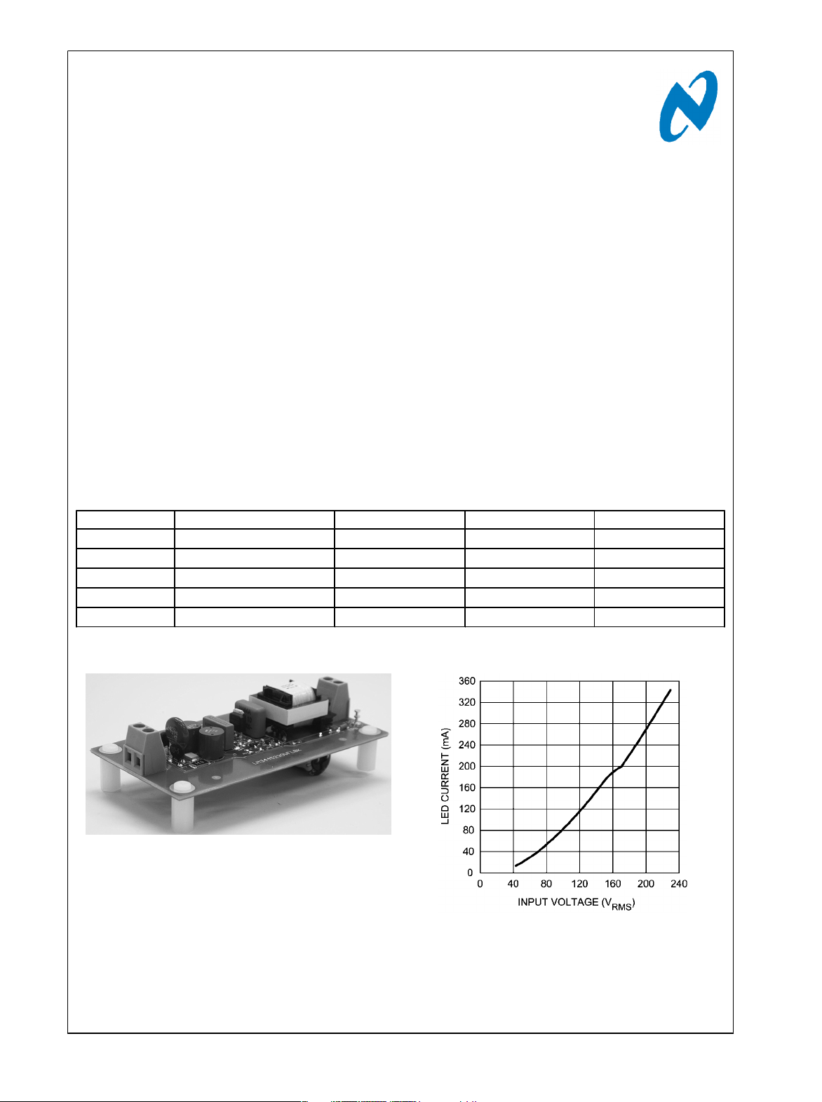
Demo Board
30126904
RMS
230 V
RMS
Dimming Characteristics
265 V
RMS
30126924
© 2010 National Semiconductor Corporation 301269 www.national.com
Page 3
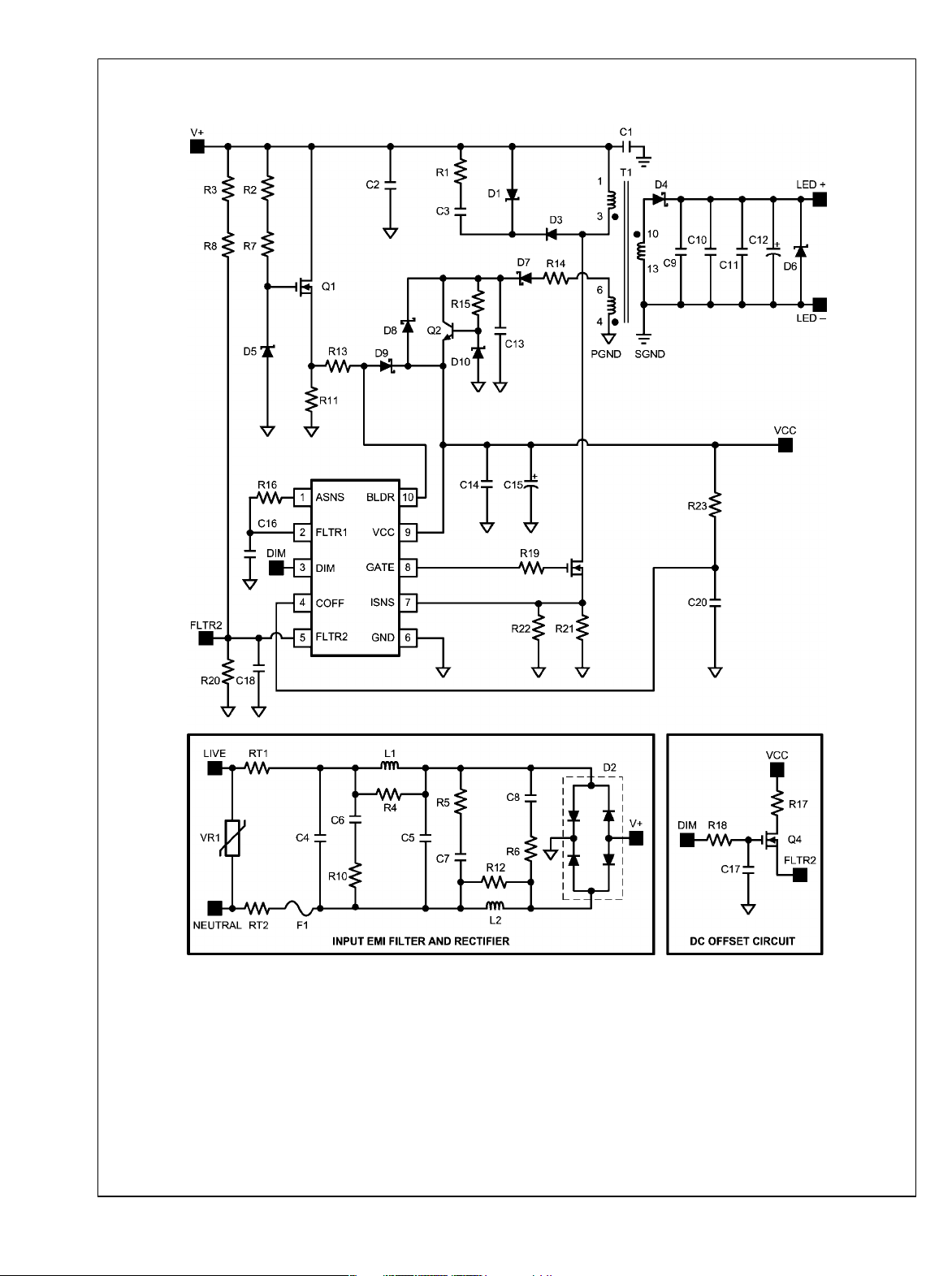
LM3445 230VAC, 8W Isolated Flyback LED Driver Demo Board Schematic
AN-2069
Warning:
Warning:
Warning:
www.national.com 2
The LM3445 evaluation board has exposed high voltage components that present a shock hazard. Caution must be taken when handling the evaluation
board. Avoid touching the evaluation board and removing any cables while the evaluation board is operating.
The ground connection on the evaluation board is NOT referenced to earth ground. If an oscilloscope ground lead is connected to the evaluation
board ground test point for analysis and the mains AC power is applied (without any isolation), the fuse (F1) will fail open. For bench evaluation, either
the input AC power source or the bench measurement equipment should be isolated from the earth ground connection. Isolating the evaliation board
(using 1:1 isolation line isolation transformer) rather than the oscilloscope is highly recommended.
The LM3445 evaluation board should not be powered with an open load. For proper operation, ensure that the desired number of LEDs are connected
at the output before applying power to the evaluation board.
30126901
Page 4
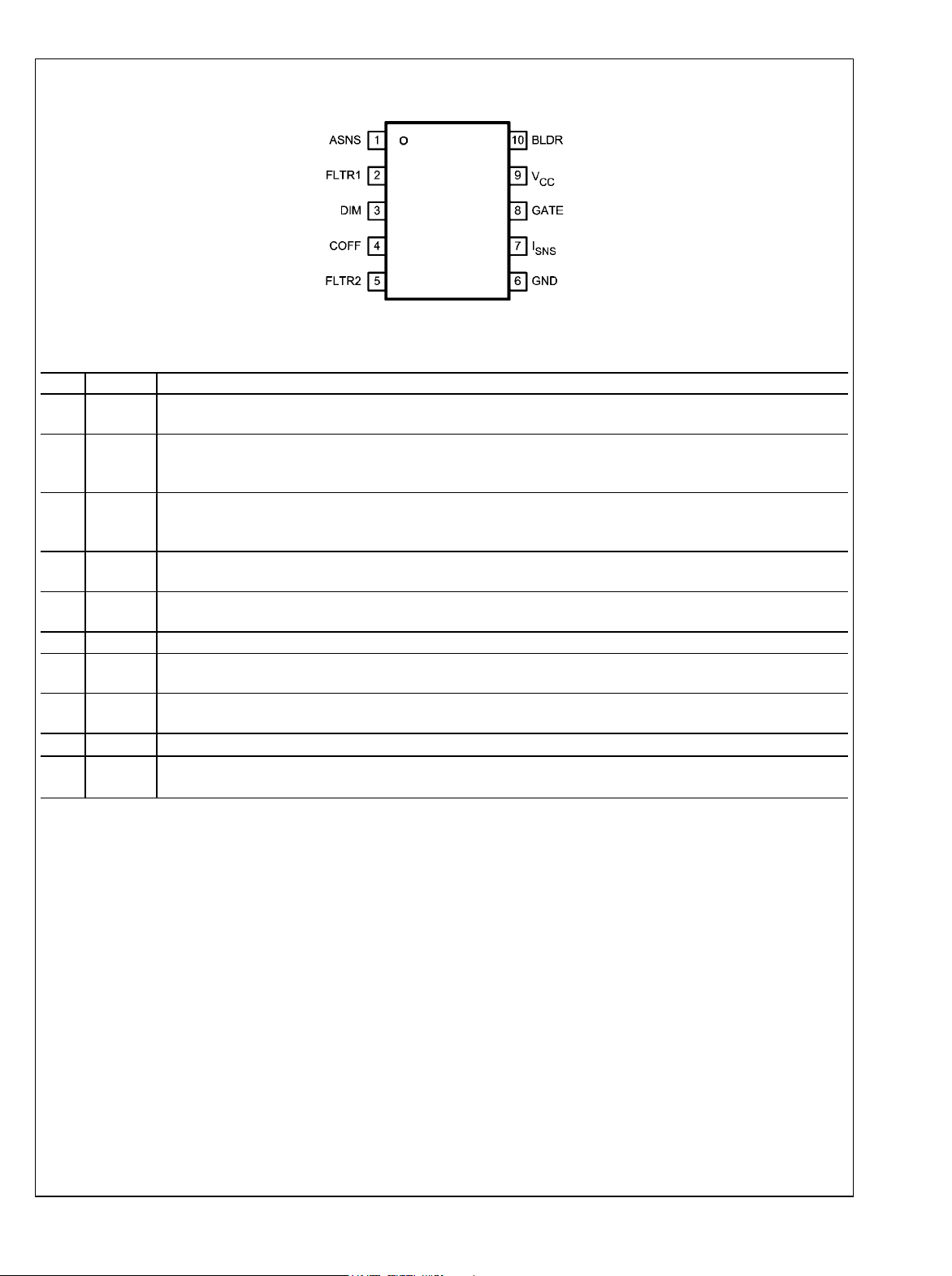
LM3445 Device Pin-Out
30126902
Pin Description 10 Pin MSOP
Pin # Name Description
1 ASNS PWM output of the triac dim decoder circuit. Outputs a 0 to 4V PWM signal with a duty cycle proportional to the triac
dimmer on-time.
2 FLTR1 First filter input. The 120Hz PWM signal from ASNS is filtered to a DC signal and compared to a 1 to 3V, 5.85 kHz
ramp to generate a higher frequency PWM signal with a duty cycle proportional to the triac dimmer firing angle. Pull
above 4.9V (typical) to tri-state DIM.
3 DIM Input/output dual function dim pin. This pin can be driven with an external PWM signal to dim the LEDs. It may also
be used as an output signal and connected to the DIM pin of other LM3445 or LED drivers to dim multiple LED
circuits simultaneously.
4 COFF OFF time setting pin. A user set current and capacitor connected from the output to this pin sets the constant OFF
time of the switching controller.
5 FLTR2 Second filter input. A capacitor tied to this pin filters the PWM dimming signal to supply a DC voltage to control the
LED current. Could also be used as an analog dimming input.
6 GND Circuit ground connection.
7 ISNS LED current sense pin. Connect a resistor from main switching MOSFET source, ISNS to GND to set the maximum
LED current.
8 GATE Power MOSFET driver pin. This output provides the gate drive for the power switching MOSFET of the buck
controller.
9 V
10 BLDR Bleeder pin. Provides the input signal to the angle detect circuitry as well as a current path through a switched
Input voltage pin. This pin provides the power for the internal control circuitry and gate driver.
CC
230Ω resistor to ensure proper firing of the triac dimmer.
AN-2069
3 www.national.com
Page 5

Bill of Materials
Designator Description Manufacturer Part Number RoHS
AN-2069
AA1 Printed Circuit Board - Y
U1 Triac Dimmable Offline LED Driver, PowerWise National
Semiconductor
C1 Ceramic, X7R, 250VAC, 10% Murata Electronics
North America
C2 Ceramic, Polypropylene, 400VDC, 10% WIMA MKP10-.033/400/5P10 Y
C3 CAP, CERM, 330pF, 630V, +/-5%, C0G/NP0, 1206 TDK C3216C0G2J331J Y
C4 Ceramic, X7R, 250V, X2, 10%, 2220 Murata Electronics
North America
C5 CAP, Film, 0.033µF, 630V, +/-10%, TH EPCOS Inc B32921C3333K Y
C6 CAP, CERM, 0.015µF, 500V, +/-10%, X7R, 1812 Vishay/Vitramon VJ1812Y223KBEAT4X Y
C7-DNP CAP, CERM, 0.1µF, 630V, +/-10%, X7R, 1812 MuRata GRM43DR72J104KW01L Y
C8 CAP, CERM, 0.1µF, 630V, +/-10%, X7R, 1812 MuRata GRM43DR72J104KW01L Y
C9, C11 CAP, CERM, 1µF, 50V, +/-10%, X7R, 1210 MuRata GRM32RR71H105KA01L Y
C10 CAP, CERM, 0.47µF, 50V, +/-10%, X7R, 0805 MuRata GRM21BR71H474KA88L Y
C12 Aluminium Electrolytic, 680uF, 35V, 20%, Nichicon UHE1V681MHD6 Y
C13 CAP, CERM, 1µF, 35V, +/-10%, X7R, 0805 Taiyo Yuden GMK212B7105KG-T Y
C14 CAP, CERM, 0.1µF, 25V, +/-10%, X7R, 0603 MuRata GRM188R71E104KA01D Y
C15 CAP, TANT, 47uF, 16V, +/-10%, 0.35 ohm, 6032-28
SMD
C16 CAP, CERM, 0.47µF, 16V, +/-10%, X7R, 0603 MuRata GRM188R71C474KA88D Y
C17 CAP, CERM, 0.22µF, 16V, +/-10%, X7R, 0603 TDK C1608X7R1C224K Y
C18 CAP, CERM, 2200pF, 50V, +/-10%, X7R, 0603 MuRata GRM188R71H222KA01D Y
C20 CAP, CERM, 330pF, 50V, +/-5%, C0G/NP0, 0603 MuRata GRM1885C1H331JA01D Y
D1 DIODE TVS 250V 600W UNI 5% SMD Littelfuse P6SMB250A Y
D2 Diode, Switching-Bridge, 600V, 0.8A, MiniDIP Diodes Inc. HD06-T Y
D3 Diode, Silicon, 1000V, 1A, SOD-123 Comchip Technology CGRM4007-G Y
D4 Diode, Schottky, 100V, 1A, SMA STMicroelectronics STPS1H100A Y
D5, D10 Diode, Zener, 13V, 200mW, SOD-323 Diodes Inc DDZ13BS-7 Y
D6 Diode, Zener, 36V, 550mW, SMB ON Semiconductor 1SMB5938BT3G Y
D7, D8, D9 Diode, Schottky, 100V, 150 mA, SOD-323 STMicroelectronics BAT46JFILM Y
F1 Fuse, 500mA, 250V, Time-Lag, SMT Littelfuse Inc 0443.500DR Y
H1, H2, H5, H6 Standoff, Hex, 0.5"L #4-40 Nylon Keystone 1902C Y
H3, H4, H7, H8 Machine Screw, Round, #4-40 x 1/4, Nylon, Philips
panhead
J1, J2 Conn Term Block, 2POS, 5.08mm PCB Phoenix Contact 1715721 Y
L1, L2 Inductor, Radial Lead Inductors, Shielded, 4.7mH,
130mA, 12.20ohm, 7.5mm Radial,
LED+, LED-,
TP7, TP8
Q1 MOSFET, N-CH, 600V, 200mA, SOT-223 Fairchild
Q2 Transistor, NPN, 300V, 500mA, SOT-23 Diodes Inc. MMBTA42-7-F Y
Q3 MOSFET, N-CH, 650V, 800mA, IPAK Infineon
Q4 MOSFET N-CH 100V 170MA SOT23-3 Diodes Inc. BSS123-7-F Y
R1 RES, 221 ohm, 1%, 0.25W, 1206 Vishay-Dale CRCW1206221RFKEA Y
R2, R7 RES, 200k ohm, 1%, 0.25W, 1206 Vishay-Dale CRCW1206200KFKEA Y
R3, R8 RES, 309k ohm, 1%, 0.25W, 1206 Vishay-Dale CRCW1206309KFKEA Y
Terminal, 22 Gauge Wire, Terminal, 22 Guage Wire 3M 923345-02-C Y
AVX TPSC476K016R0350 Y
B&F Fastener Supply NY PMS 440 0025 PH Y
TDK Corporation TSL0808RA-472JR17-PF Y
Semiconductor
Technologies
LM3445MM Y
DE1E3KX332MA5BA01 Y
GA355DR7GF472KW01L Y
FQT1N60CTF_WS Y
SPU01N60C3 Y
www.national.com 4
Page 6
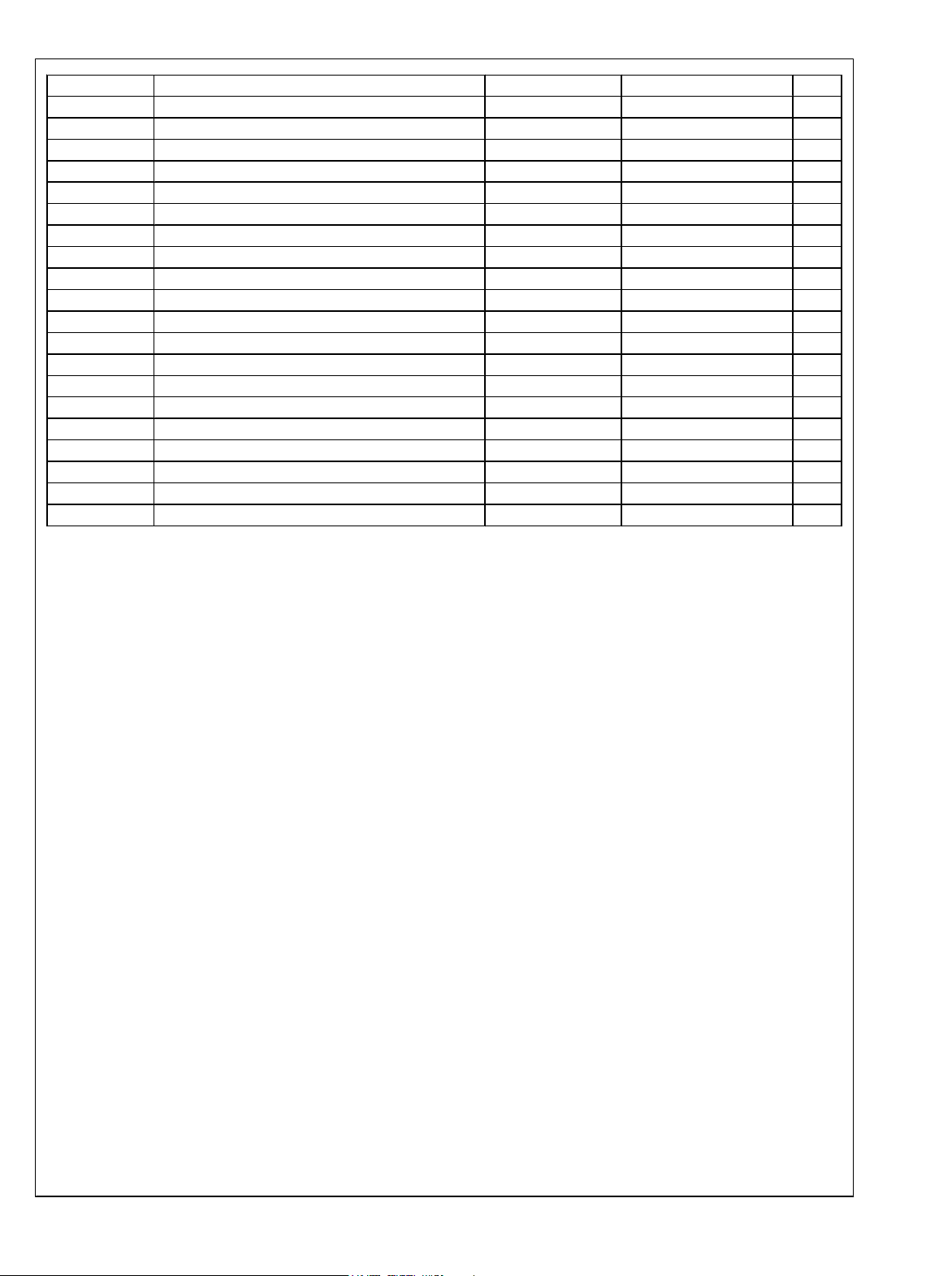
Designator Description Manufacturer Part Number RoHS
R4, R12 RES, 10k ohm, 5%, 0.25W, 1206 Vishay-Dale CRCW120610K0JNEA Y
R5-DNP RES, 680 ohm, 5%, 1W, 2512 Vishay/Dale CRCW2512680RJNEG Y
R6 RES, 820 ohm, 5%, 1W, 2512 Vishay/Dale CRCW2512820RJNEG Y
R10 RES, 430 ohm, 5%, 1W, 2512 Vishay/Dale CRCW2512430RJNEG Y
R11 RES, 49.9k ohm, 1%, 0.125W, 0805 Vishay-Dale CRCW080549K9FKEA Y
R13 RES, 33.0 ohm, 1%, 0.25W, 1206 Vishay-Dale CRCW120633R0FKEA Y
R14 RES, 10 ohm, 5%, 0.125W, 0805 Vishay-Dale CRCW080510R0JNEA Y
R15 RES, 10.0k ohm, 1%, 0.1W, 0603 Vishay-Dale CRCW060310K0FKEA Y
R16 RES, 280k ohm, 1%, 0.1W, 0603 Vishay-Dale CRCW0603280KFKEA Y
R17 RES, 475k ohm, 1%, 0.1W, 0603 Vishay-Dale CRCW0603475KFKEA Y
R18 RES, 49.9k ohm, 1%, 0.1W, 0603 Vishay-Dale CRCW060349K9FKEA Y
R19 RES, 10 ohm, 5%, 0.1W, 0603 Vishay-Dale CRCW060310R0JNEA Y
R20 RES, 1.91k ohm, 1%, 0.1W, 0603 Vishay-Dale CRCW06031K91FKEA Y
R21 RES, 2.70 ohm, 1%, 0.25W, 1206 Panasonic ERJ-8RQF2R7V Y
R22 RES, 10.7 ohm, 1%, 0.125W, 0805 Vishay-Dale CRCW080510R7FKEA Y
R23 RES, 324k ohm, 1%, 0.1W, 0603 Vishay-Dale CRCW0603324KFKEA Y
RT1, RT2 Current Limitor Inrush, 60Ohm, 20%, 5mm Raidal Cantherm MF72-060D5 Y
T1 FLBK TFR, 2.07 mH, Np=140T, Ns=26T, Na= 20T Wurth Elektornik 750815040 REV 1 Y
TP9, TP10 Terminal, Turret, TH, Double Keystone Electronics 1502-2 Y
VR1 Varistor 275V 55J 10mm DISC EPCOS Inc S10K275E2 Y
AN-2069
5 www.national.com
Page 7

Transformer Design
Mfg: Wurth Electronics, Part #: 750815040 Rev. 01
AN-2069
Parameter Test Conditions Value
D.C. Resistance (3-1) 20°C
D.C. Resistance (6-4) 20°C
D.C. Resistance (10-13) 20°C
Inductance (3-1) 10 kHz, 100 mVAC 2.12 mH ± 10%
Inductance (6-4) 10 kHz, 100 mVAC 46.50 µH ± 10%
Inductance (10-13) 10 kHz, 100 mVAC 74.00 µH ± 10%
Leakage Inductance (3-1) 100 kHz, 100 mAVAC (tie 6+4, 10+13) 18.0 µH Typ., 22.60 µH Max.
Dielectric (1-13) tie (3+4), 4500 VAC, 1 second 4500 VAC, 1 minute
Turns Ratio (3-1):(6-4) 7:1 ± 1%
Turns Ratio (3-1):(10:13) 5.384:1 ± 1%
1.91 Ω ± 10%
0.36 Ω ± 10%
0.12 Ω ± 10%
30126909
www.national.com 6
Page 8

Demo Board Wiring Overview
AN-2069
Wiring Connection Diagram
Test Point Name I/O Description
TP8, TP10 LED + Output LED Constant Current Supply
Supplies voltage and constant-current to anode of LED string.
TP7, TP9 LED - Output LED Return Connection (not GND)
Connects to cathode of LED string. Do NOT connect to GND.
J1-1 LINE Input AC Line Voltage
Connects directly to AC line or output of TRIAC dimmer of a 230VAC system.
J1-2 NEUTRAL Input AC Neutral
Connects directly to AC neutral of a 230VAC system.
Demo Board Assembly
30126903
Top View
Bottom View
7 www.national.com
30126905
30126906
Page 9

Typical Performance Characteristics (Note 1, Note 2, Note 3)
180 190 200 210 220 230 240 250 260
0.76
0.77
0.78
0.79
0.80
0.81
0.82
0.83
EFFICIENCY
INPUT VOLTAGE (V
RMS
)
10 LEDs
8 LEDs
6 LEDs
4 LEDs
180 190 200 210 220 230 240 250 260
0.60
0.64
0.68
0.73
0.77
0.81
0.85
0.89
0.93
0.97
EFFICIENCY
INPUT VOLTAGE (V
RMS
)
Mod C (10 LEDs)
Mod B (8 LEDs)
Original (6 LEDs)
Mod A (4 LEDs)
180 190 200 210 220 230 240 250 260
50
150
250
350
450
550
650
LED CURRENT (mA)
INPUT VOLTAGE (V
RMS
)
4 LEDs
8 LEDs
10 LEDs
6 LEDs
180 190 200 210 220 230 240 250 260
100
150
200
250
300
350
400
450
500
550
600
LED CURRENT (mA)
INPUT VOLTAGE (V
RMS
)
Mod C (10 LEDs)
Mod B (8 LEDs)
Original (6 LEDs)
Mod A (4 LEDs)
180 190 200 210 220 230 240 250 260
0.920
0.924
0.928
0.932
0.936
0.940
0.944
0.948
0.952
0.956
POWER FACTOR
INPUT VOLTAGE (V
RMS
)
10 LEDs
8 LEDs
4 LEDs
6 LEDs
180 190 200 210 220 230 240 250 260
0.60
0.64
0.68
0.73
0.77
0.81
0.85
0.89
0.93
0.97
POWER FACTOR
INPUT VOLTAGE (V
RMS
)
Mod C (10 LEDs)
Mod B (8 LEDs)
Original (6 LEDs)
Mod A (4 LEDs)
AN-2069
Efficiency vs. Line Voltage
Original Circuit
LED Current vs. Line Voltage
Original Circuit
30126910
Efficiency vs. Line Voltage
Modified Circuits
30126914
LED Current vs. Line Voltage
Modified Circuits
Power Factor vs. Line Voltage
www.national.com 8
Original Circuit
30126911
30126912
30126915
Power Factor vs. Line Voltage
Modified Circuits
30126916
Page 10

180 190 200 210 220 230 240 250 260
2
3
4
5
6
7
8
9
10
11
12
OUTPUT POWER (W)
LINE VOLTAGE (V
RMS
)
10 LEDs
8 LEDs
4 LEDs
6 LEDs
180 190 200 210 220 230 240 250 260
0.0
2.5
5.0
7.5
10.0
12.5
15.0
17.5
20.0
22.5
25.0
OUTPUT POWER (W)
INPUT VOLTAGE (V
RMS
)
Mod C (10 LEDs)
Mod B (8 LEDs)
Original (6 LEDs)
Mod A (4 LEDs)
AN-2069
Output Power vs. Line Voltage
Original Circuit
Line Voltage and Line Current
(VIN = 230V
, 6 LEDs, I
RMS
LED
= 350mA)
30126913
Output Power vs. Line Voltage
Modified Circuits
Output Voltage and LED Current
(VIN = 230V
, 6 LEDs, I
RMS
= 350mA)
LED
30126917
Ch1: Line Voltage (100 V/div); Ch3: Line Current
(20 mA/div); Time (4 ms/div)
Power MOSFET Drain and ISNS (Pin-7) Voltage
(VIN = 230V
Ch1: Drain Voltage (100V/div); Ch4: ISNS Voltage
Note 1: Original Circuit (6 LEDs operating at 350mA): R21 = 2.7Ω; Modification A (10 LEDs operating at 375mA): R21 = 1.8Ω; Modification B (8 LEDs operating
at 350mA): R21 = 2.2Ω; Modification C (4 LEDs operating at 315mA): R21 = 3.9Ω
Note 2: The output power can be varied to acheive desired LED current by interpolating R14 values between the maximum of 3.9 Ω and minimum of 1.8 Ω
Note 3: The maximum output voltage is clamped to 36 V. For operating LED string voltage > 36 V, replace D6 with suitable alternative
(500 mV/div); Time (4 µs/div)
, 6 LEDs, I
RMS
LED
= 350mA)
30126918
30126921
Ch1: Output Voltage (10 V/div); Ch3: LED Current
(100 mA/div); Time (4 ms/div)
FLTR2 (Pin-5) and ISNS (Pin-7) Voltage
(VIN=230V
, 6 LEDs, I
RMS
= 350mA
LED
Ch1: FLTR2 Voltage (200 mV/div); ISNS Voltage
(200 mV/div); Time (4 µs/div)
9 www.national.com
30126920
30126922
Page 11

PCB Layout
AN-2069
Top Layer
Bottom Layer
30126907
30126908
www.national.com 10
Page 12

AN-2069
Experimental Results
The LED driver is designed to accurately emulate an incandescent light bulb and therefore behave as an emulated
resistor. The resistor value is determined based on the LED
string configuration and the desired output power. The circuit
then operates in open-loop, with a fixed duty cycle based on
a constant on-time and constant off-time that is set by selecting appropriate circuit components. Like an incandescent
lamp, the driver is compatible with both forward and reverse
phase dimmers.
NON-DIMMING PERFORMANCE
In steady state, the LED string voltage is measured to be 20.5
V and the average LED current is measured as 350 mA. The
measured to be 194 mA
ripple is a function of the value of energy storage capacitors
connected across the output port and the TRIAC firing angle.
The ripple current can be reduced by increasing the value of
energy storage capacitor or by increasing the LED string voltage. With TRIAC dimmers, the ripple magnitude is directly
proportional to the input power and therefore reduces at lower
LED current.
The LED driver switching frequency is measured to be close
to the specified 67 kHz. The circuit operates with a constant
duty cycle of 0.21 and consumes near 8.75 W of input power.
The driver steady state performance for an LED string consisting of 6 series LEDs without using a triac dimmer is
summarized in the following table.
at full load. The magnitude of the
pk-pk
100 Hz current ripple flowing through the LED string was
MEASURED EFFICIENCY AND LINE REGULATION (6 LEDS, NO TRIAC DIMMER)
VIN (V
) IIN (mA
RMS
) PIN(W) V
RMS
(V) I
OUT
(mA) P
LED
(W) Efficiency (%) Power Factor
OUT
180 31.73 5.35 19.67 221.64 4.36 81.4 0.9375
190 33.39 5.96 19.85 244.82 4.86 81.5 0.9394
200 35.11 6.61 20.04 269.16 5.39 81.6 0.9493
210 36.85 7.30 20.22 294.82 5.96 81.6 0.9493
220 38.53 8.01 20.40 321.26 6.55 81.8 0.9451
230 40.18 8.75 20.56 348.70 7.17 82.0 0.9463
240 41.75 9.50 20.74 375.70 7.79 82.0 0.9477
250 43..39 10.30 20.90 404.82 8.46 82.1 0.9490
260 45.07 11.14 21.05 434.48 9.15 82.0 0.9500
DIMMING PERFORMANCE
The LED driver is capable of matching or exceeding the dimming performance of an incandescent lamp. Using a simple
rotary TRIAC dimmer, smooth and near logarithmic dimming
performance is achieved. By varying the firing angle of the
MEASURED DIMMING PERFORMANCE
VIN (V
) VO (V) I
RMS
229.39 20.51 343.1 7.04
220.47 20.35 320.8 6.53
210.24 20.16 294.8 5.94
199.05 19.98 266.8 5.33
190.32 19.80 245.8 4.87
180.33 19.61 222.7 4.37
170.51 19.42 200.1 3.89
156.39 19.31 187.4 3.62
149.11 19.15 171.6 3.29
140.35 18.97 154.0 2.92
129.61 18.75 133.1 2.50
119.7 18.53 115.3 2.14
110.17 18.33 99.1 1.82
100.55 18.11 83.5 1.51
90.75 17.87 68.8 1.23
79.72 17.59 53.1 0.93
70.42 17.34 40.8 0.71
60.91 17.08 30.1 0.81
49.94 16.77 19.8 0.33
45.04 16.64 16.0 0.27
TRIAC dimmer and measuring the corresponding input and
output parameters, the dimming performance of the demonstration board driving 6 LEDs is summarized in the table
below.
(mA) P
LED
OUT
(W)
11 www.national.com
Page 13

AN-2069
CURRENT THD
Dimming Characteristics
The LED driver is able to achieve close to unity power factor
(P.F. ~ 0.94) which meets Energy Star requirements. This
design also exhibits low current harmonics as a percentage
Current Harmonic vs. EN/IEC61000-3-2 Class C Limits
30126924
of the fundamental current (as shown in the following figure)
and therefore meets the requirements of the IEC 61000-3-2
Class-3 standard.
30126923
www.national.com 12
Page 14

Circuit Operation With Rotary Forward Phase Triac Dimmer
AN-2069
Input waveforms at full brightness setting
Ch1: Input Voltage (100 V/div); Ch3: Input Current
30126925
(20 mA/div); Time (4 ms/div)
Input waveforms at half brightness setting (90° firing angle)
Output waveforms at full brightness setting
Ch1: Output Voltage (10 V/div); LED Current
30126928
(100 mA/div); Time (4 ms/div)
Output waveforms at half brightness setting (90° firing angle)
Ch1: Input Voltage (100 V/div); Ch3: Input Current
30126926
(20 mA/div); Time (4 ms/div)
Input waveforms at minimum brightness setting
Ch1: Input Voltage (100 V/div); Ch3: Input Current
30126927
(20 mA/div); Time (4 ms/div)
Ch1: Output Voltage (10 V/div); LED Current
30126929
(100 mA/div); Time (4 ms/div)
Output waveforms at minimum brightness setting
Ch1: Output Voltage (10 V/div); LED Current
30126930
(100 mA/div); Time (4 ms/div)
13 www.national.com
Page 15

Electromagnetic Interference (EMI)
The EMI input filter of this evaluation board is configured as
AN-2069
shown in the following circuit diagram.
FIGURE 1. Input EMI Filter and Rectifier Circuit
30126931
In order to get a quick estimate of the EMI filter performance,
only the PEAK conductive EMI scan was measured and the
FIGURE 2. Peak Conductive EMI scan per CISPR-22, Class B Limits
Note 4: CISPR 15 compliance pending
data was compared to the Class B conducted EMI limits published in FCC – 47, section 15.(Note 4)
30126932
www.national.com 14
Page 16

Thermal Analysis
The board temperature was measured using an IR camera
(HIS-3000, Wahl) while running under the following conditions:
VIN = 230 V
RMS
I
= 348 mA
LED
# of LEDs = 6
P
= 7.2 W
OUT
The results are shown in the following figures.
AN-2069
FIGURE 3. Top Side Thermal Scan
30126933
FIGURE 4. Bottom Side Thermal Scan
15 www.national.com
30126934
Page 17

Circuit Analysis and Explanations
INJECTING LINE VOLTAGE INTO FILTER-2 (ACHIEVING
AN-2069
PFC > 0.94)
If a small portion (750mV to 1.00V) of line voltage is injected
at FLTR2 of the LM3445, the circuit is essentially turned into
a constant power flyback as shown in Figure 5.
FIGURE 5. Line Voltage Injection Circuit
The LM3445 works as a constant off-time controller normally,
but by injecting the 1.0VPk rectified AC voltage into the FLTR2
30126935
pin, the on-time can be made to be constant. With a DCM
Flyback, Δi needs to increase as the input voltage line increases. Therefore a constant on-time (since inductor L is
constant) can be obtained.
By using the line voltage injection technique, the FLTR2 pin
has the voltage wave shape shown in Figure 6 on it with no
triac dimmer in-line. Voltage at V
below 1.25V. At 1.25V current limit is tripped. C11 is small
peak should be kept
FLTR2
enough not to distort the AC signal but adds a little filtering.
Although the on-time is probably never truly constant, it can
be observed in Figure 7 how (by adding the rectified voltage)
the on-time is adjusted.
30126937
FIGURE 6. FLTR2 Waveform with No Dimmer
For this evaluation board, the following resistor values are
used:
R3 = R8 = 309 kΩ
R20 = 1.91 kΩ
Therefore the voltages observed on the FLTR2 pin will be as
follows for listed input voltages:
For VIN = 180V
For VIN = 230V
For VIN = 265V
RMS
RMS
RMS
, V
FLTR2, Pk
, V
FLTR2, Pk
, V
FLTR2, Pk
= 0.78V
= 1.00V
= 1.15V
Using this technique, a power factor greater than 0.94 can be
achieved without additional passive active power factor control (PFC) circuitry.
FIGURE 7. Typical Operation of FLTR2 Pin
www.national.com 16
30126936
Page 18

Notes
AN-2069
17 www.national.com
Page 19

Notes
For more National Semiconductor product information and proven design tools, visit the following Web sites at:
www.national.com
Products Design Support
Amplifiers www.national.com/amplifiers WEBENCH® Tools www.national.com/webench
Audio www.national.com/audio App Notes www.national.com/appnotes
Clock and Timing www.national.com/timing Reference Designs www.national.com/refdesigns
Data Converters www.national.com/adc Samples www.national.com/samples
Interface www.national.com/interface Eval Boards www.national.com/evalboards
LVDS www.national.com/lvds Packaging www.national.com/packaging
Power Management www.national.com/power Green Compliance www.national.com/quality/green
Switching Regulators www.national.com/switchers Distributors www.national.com/contacts
LDOs www.national.com/ldo Quality and Reliability www.national.com/quality
LED Lighting www.national.com/led Feedback/Support www.national.com/feedback
Voltage References www.national.com/vref Design Made Easy www.national.com/easy
PowerWise® Solutions www.national.com/powerwise Applications & Markets www.national.com/solutions
Serial Digital Interface (SDI) www.national.com/sdi Mil/Aero www.national.com/milaero
Temperature Sensors www.national.com/tempsensors SolarMagic™ www.national.com/solarmagic
PLL/VCO www.national.com/wireless PowerWise® Design
University
www.national.com/training
THE CONTENTS OF THIS DOCUMENT ARE PROVIDED IN CONNECTION WITH NATIONAL SEMICONDUCTOR CORPORATION
(“NATIONAL”) PRODUCTS. NATIONAL MAKES NO REPRESENTATIONS OR WARRANTIES WITH RESPECT TO THE ACCURACY
OR COMPLETENESS OF THE CONTENTS OF THIS PUBLICATION AND RESERVES THE RIGHT TO MAKE CHANGES TO
SPECIFICATIONS AND PRODUCT DESCRIPTIONS AT ANY TIME WITHOUT NOTICE. NO LICENSE, WHETHER EXPRESS,
IMPLIED, ARISING BY ESTOPPEL OR OTHERWISE, TO ANY INTELLECTUAL PROPERTY RIGHTS IS GRANTED BY THIS
DOCUMENT.
TESTING AND OTHER QUALITY CONTROLS ARE USED TO THE EXTENT NATIONAL DEEMS NECESSARY TO SUPPORT
NATIONAL’S PRODUCT WARRANTY. EXCEPT WHERE MANDATED BY GOVERNMENT REQUIREMENTS, TESTING OF ALL
PARAMETERS OF EACH PRODUCT IS NOT NECESSARILY PERFORMED. NATIONAL ASSUMES NO LIABILITY FOR
APPLICATIONS ASSISTANCE OR BUYER PRODUCT DESIGN. BUYERS ARE RESPONSIBLE FOR THEIR PRODUCTS AND
APPLICATIONS USING NATIONAL COMPONENTS. PRIOR TO USING OR DISTRIBUTING ANY PRODUCTS THAT INCLUDE
NATIONAL COMPONENTS, BUYERS SHOULD PROVIDE ADEQUATE DESIGN, TESTING AND OPERATING SAFEGUARDS.
EXCEPT AS PROVIDED IN NATIONAL’S TERMS AND CONDITIONS OF SALE FOR SUCH PRODUCTS, NATIONAL ASSUMES NO
LIABILITY WHATSOEVER, AND NATIONAL DISCLAIMS ANY EXPRESS OR IMPLIED WARRANTY RELATING TO THE SALE
AND/OR USE OF NATIONAL PRODUCTS INCLUDING LIABILITY OR WARRANTIES RELATING TO FITNESS FOR A PARTICULAR
PURPOSE, MERCHANTABILITY, OR INFRINGEMENT OF ANY PATENT, COPYRIGHT OR OTHER INTELLECTUAL PROPERTY
RIGHT.
LIFE SUPPORT POLICY
NATIONAL’S PRODUCTS ARE NOT AUTHORIZED FOR USE AS CRITICAL COMPONENTS IN LIFE SUPPORT DEVICES OR
SYSTEMS WITHOUT THE EXPRESS PRIOR WRITTEN APPROVAL OF THE CHIEF EXECUTIVE OFFICER AND GENERAL
COUNSEL OF NATIONAL SEMICONDUCTOR CORPORATION. As used herein:
Life support devices or systems are devices which (a) are intended for surgical implant into the body, or (b) support or sustain life and
whose failure to perform when properly used in accordance with instructions for use provided in the labeling can be reasonably expected
to result in a significant injury to the user. A critical component is any component in a life support device or system whose failure to perform
can be reasonably expected to cause the failure of the life support device or system or to affect its safety or effectiveness.
National Semiconductor and the National Semiconductor logo are registered trademarks of National Semiconductor Corporation. All other
brand or product names may be trademarks or registered trademarks of their respective holders.
Copyright© 2010 National Semiconductor Corporation
For the most current product information visit us at www.national.com
National Semiconductor
Americas Technical
Support Center
Email: support@nsc.com
AN-2069 LM3445 - 230VAC, 6W- 15W Isolated Flyback LED Driver
www.national.com
Tel: 1-800-272-9959
National Semiconductor Europe
Technical Support Center
Email: europe.support@nsc.com
National Semiconductor Asia
Pacific Technical Support Center
Email: ap.support@nsc.com
National Semiconductor Japan
Technical Support Center
Email: jpn.feedback@nsc.com
Page 20

IMPORTANT NOTICE
Texas Instruments Incorporated and its subsidiaries (TI) reserve the right to make corrections, modifications, enhancements, improvements,
and other changes to its products and services at any time and to discontinue any product or service without notice. Customers should
obtain the latest relevant information before placing orders and should verify that such information is current and complete. All products are
sold subject to TI’s terms and conditions of sale supplied at the time of order acknowledgment.
TI warrants performance of its hardware products to the specifications applicable at the time of sale in accordance with TI’s standard
warranty. Testing and other quality control techniques are used to the extent TI deems necessary to support this warranty. Except where
mandated by government requirements, testing of all parameters of each product is not necessarily performed.
TI assumes no liability for applications assistance or customer product design. Customers are responsible for their products and
applications using TI components. To minimize the risks associated with customer products and applications, customers should provide
adequate design and operating safeguards.
TI does not warrant or represent that any license, either express or implied, is granted under any TI patent right, copyright, mask work right,
or other TI intellectual property right relating to any combination, machine, or process in which TI products or services are used. Information
published by TI regarding third-party products or services does not constitute a license from TI to use such products or services or a
warranty or endorsement thereof. Use of such information may require a license from a third party under the patents or other intellectual
property of the third party, or a license from TI under the patents or other intellectual property of TI.
Reproduction of TI information in TI data books or data sheets is permissible only if reproduction is without alteration and is accompanied
by all associated warranties, conditions, limitations, and notices. Reproduction of this information with alteration is an unfair and deceptive
business practice. TI is not responsible or liable for such altered documentation. Information of third parties may be subject to additional
restrictions.
Resale of TI products or services with statements different from or beyond the parameters stated by TI for that product or service voids all
express and any implied warranties for the associated TI product or service and is an unfair and deceptive business practice. TI is not
responsible or liable for any such statements.
TI products are not authorized for use in safety-critical applications (such as life support) where a failure of the TI product would reasonably
be expected to cause severe personal injury or death, unless officers of the parties have executed an agreement specifically governing
such use. Buyers represent that they have all necessary expertise in the safety and regulatory ramifications of their applications, and
acknowledge and agree that they are solely responsible for all legal, regulatory and safety-related requirements concerning their products
and any use of TI products in such safety-critical applications, notwithstanding any applications-related information or support that may be
provided by TI. Further, Buyers must fully indemnify TI and its representatives against any damages arising out of the use of TI products in
such safety-critical applications.
TI products are neither designed nor intended for use in military/aerospace applications or environments unless the TI products are
specifically designated by TI as military-grade or "enhanced plastic." Only products designated by TI as military-grade meet military
specifications. Buyers acknowledge and agree that any such use of TI products which TI has not designated as military-grade is solely at
the Buyer's risk, and that they are solely responsible for compliance with all legal and regulatory requirements in connection with such use.
TI products are neither designed nor intended for use in automotive applications or environments unless the specific TI products are
designated by TI as compliant with ISO/TS 16949 requirements. Buyers acknowledge and agree that, if they use any non-designated
products in automotive applications, TI will not be responsible for any failure to meet such requirements.
Following are URLs where you can obtain information on other Texas Instruments products and application solutions:
Products Applications
Audio www.ti.com/audio Communications and Telecom www.ti.com/communications
Amplifiers amplifier.ti.com Computers and Peripherals www.ti.com/computers
Data Converters dataconverter.ti.com Consumer Electronics www.ti.com/consumer-apps
DLP® Products www.dlp.com Energy and Lighting www.ti.com/energy
DSP dsp.ti.com Industrial www.ti.com/industrial
Clocks and Timers www.ti.com/clocks Medical www.ti.com/medical
Interface interface.ti.com Security www.ti.com/security
Logic logic.ti.com Space, Avionics and Defense www.ti.com/space-avionics-defense
Power Mgmt power.ti.com Transportation and Automotive www.ti.com/automotive
Microcontrollers microcontroller.ti.com Video and Imaging www.ti.com/video
RFID www.ti-rfid.com
OMAP Mobile Processors www.ti.com/omap
Wireless Connectivity www.ti.com/wirelessconnectivity
TI E2E Community Home Page e2e.ti.com
Mailing Address: Texas Instruments, Post Office Box 655303, Dallas, Texas 75265
Copyright © 2011, Texas Instruments Incorporated
 Loading...