

Page 1
GND
DIM
BOOT SW
CS
RON
LM3404/04HV
VIN
D1
L1
C
B
R
SNS
C
F
R
ON
C
IN
V
IN
I
F
VCC
LM3404, LM3404HV
www.ti.com
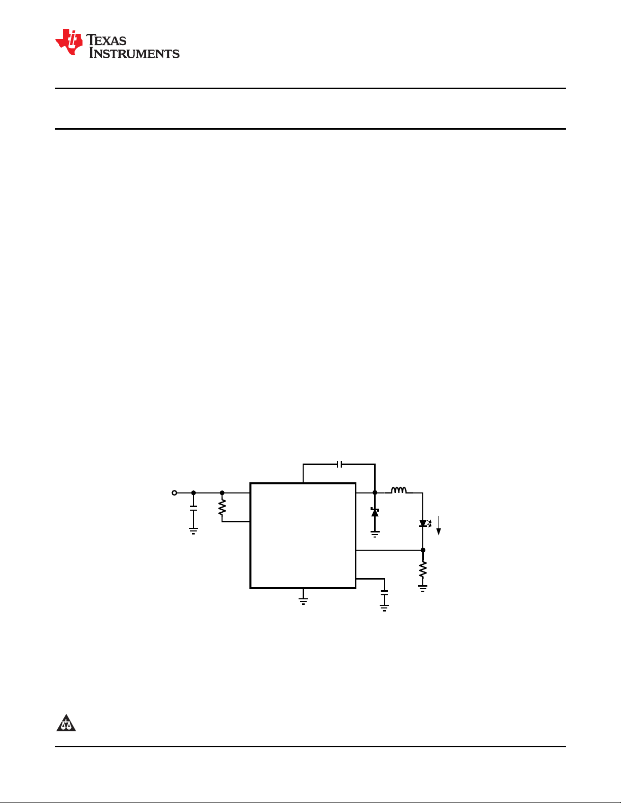
1.0A Constant Current Buck Regulator for Driving High Power LEDs
Check for Samples: LM3404, LM3404HV
1
FEATURES
2
• Integrated 1.0A MOSFET
• VINRange 6V to 42V (LM3404)
• VINRange 6V to 75V (LM3404HV)
• 1.2A Output Current Over Temperature
• Cycle-by-Cycle Current Limit
• No Control Loop Compensation Required
• Separate PWM Dimming and Low Power
Shutdown
• Supports All-ceramic Output Capacitors and
Capacitor-less Outputs
• Thermal Shutdown Protection
• SOIC-8 Package, So PowerPAD-8 Package
APPLICATIONS
• LED Driver
• Constant Current Source
• Automotive Lighting
• General Illumination
• Industrial Lighting
SNVS465F –OCTOBER 2006–REVISED MAY 2013
DESCRIPTION
The LM3404/04HV are monolithic switching
regulators designed to deliver constant currents to
high power LEDs. Ideal for automotive, industrial, and
general lighting applications, they contain a high-side
N-channel MOSFET switch with a current limit of
1.5A (typical) for step-down (Buck) regulators.
Hysteretic controlled on-time and an external resistor
allow the converter output voltage to adjust as
needed to deliver a constant current to series and
series-parallel connected LED arrays of varying
number and type. LED dimming via pulse width
modulation (PWM), broken/open LED protection, lowpower shutdown and thermal shutdown complete the
feature set.
Typical Application
1
2All trademarks are the property of their respective owners.
PRODUCTION DATA information is current as of publication date.
Products conform to specifications per the terms of the Texas
Instruments standard warranty. Production processing does not
necessarily include testing of all parameters.
Please be aware that an important notice concerning availability, standard warranty, and use in critical applications of
Texas Instruments semiconductor products and disclaimers thereto appears at the end of this data sheet.
Copyright © 2006–2013, Texas Instruments Incorporated
Page 2
SW
1
RON
2
VIN
3
BOOT
4
VCC
8
GND
7
DIM
6
CS
5
SW
1
RON
2
VIN
3
BOOT
4
VCC
8
GND
7
DIM
6
CS
5
DAP
LM3404, LM3404HV
SNVS465F –OCTOBER 2006–REVISED MAY 2013
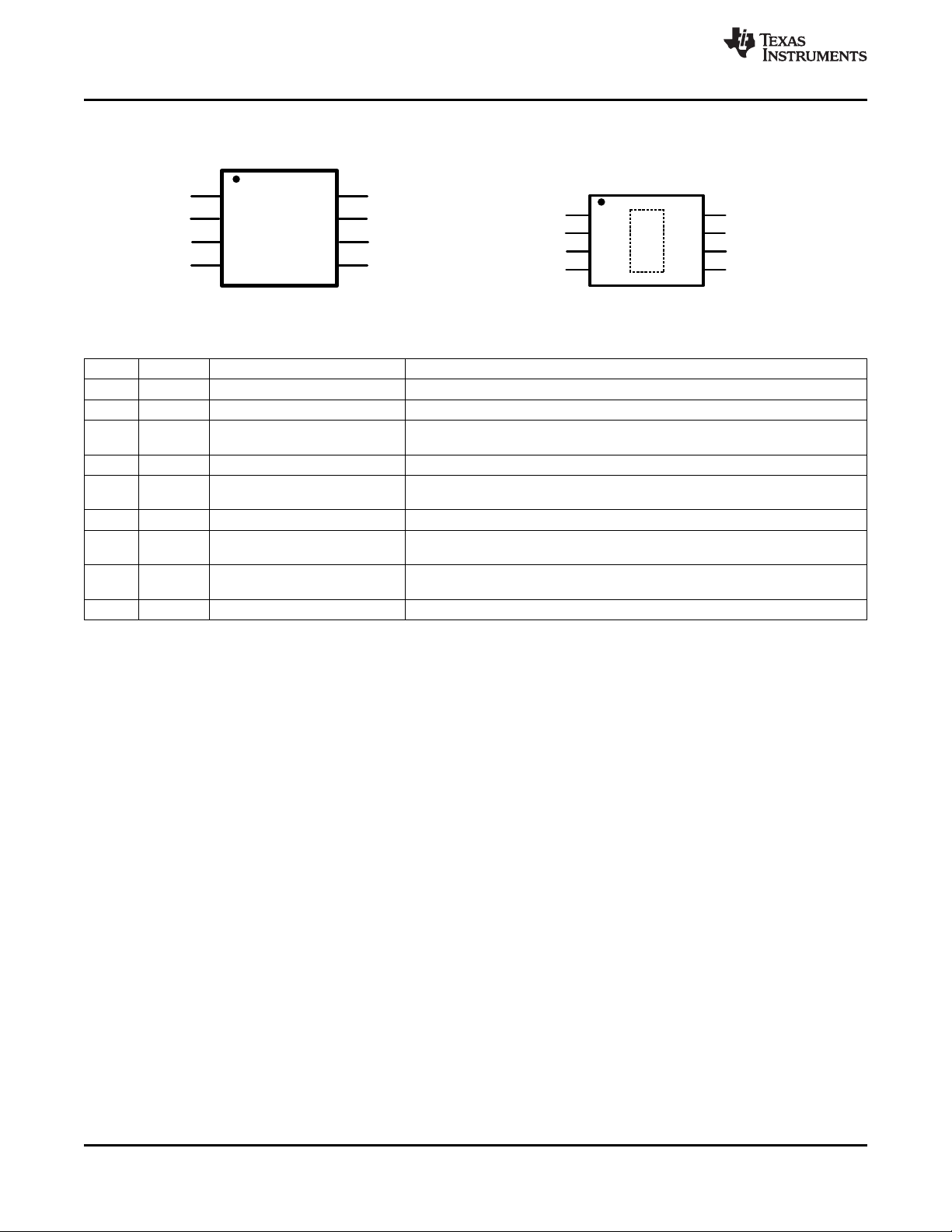
Connection Diagrams
Figure 1. 8-Lead Plastic SOIC-8 Package Figure 2. 8-Lead Plastic So PowerPAD-8 Package
PIN DESCRIPTIONS
Pin(s) Name Description Application Information
1 SW Switch pin Connect this pin to the output inductor and Schottky diode.
2 BOOT MOSFET drive bootstrap pin Connect a 10 nF ceramic capacitor from this pin to SW.
3 DIM Connect a logic-level PWM signal to this pin to enable/disable the power
4 GND Ground pin Connect this pin to system ground.
5 CS Set the current through the LED array by connecting a resistor from this pin to
6 RON On-time control pin A resistor connected from this pin to VIN sets the regulator controlled on-time.
7 VCC Output of the internal 7V linear Bypass this pin to ground with a minimum 0.1 µF ceramic capacitor with X5R or
8 VIN Nominal operating input range for this pin is 6V to 42V (LM3404) or 6V to 75V
DAP GND Thermal Pad Connect to ground. Place 4-6 vias from DAP to bottom layer ground plane.
Input for PWM dimming
Current sense feedback pin
MOSFET and reduce the average light output of the LED array.
ground.
regulator X7R dielectric.
Input voltage pin
(LM3404HV).
www.ti.com
2 Submit Documentation Feedback Copyright © 2006–2013, Texas Instruments Incorporated
Product Folder Links: LM3404 LM3404HV
Page 3

LM3404, LM3404HV
www.ti.com
These devices have limited built-in ESD protection. The leads should be shorted together or the device placed in conductive foam
during storage or handling to prevent electrostatic damage to the MOS gates.
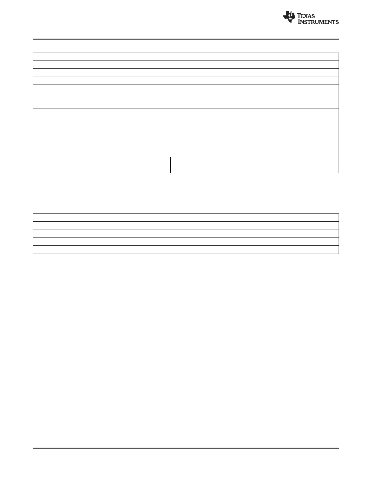
ABSOLUTE MAXIMUM RATINGS(LM3404)
(1)
SNVS465F –OCTOBER 2006–REVISED MAY 2013
If Military/Aerospace specified devices are required, please contact the Texas Instruments Semiconductor Sales
Office/ Distributors for availability and specifications.
VALUE / UNIT
VIN to GND –0.3 V to 45 V
BOOT to GND –0.3 V to 59 V
SW to GND –1.5 V to 45 V
BOOT to VCC –0.3 V to 45 V
BOOT to SW –0.3 V to 14 V
VCC to GND –0.3 V to 14 V
DIM to GND –0.3 V to 7 V
CS to GND –0.3 V to 7 V
RON to GND –0.3 V to 7 V
Junction Temperature 150°C
Storage Temp. Range –65°C to 125°C
ESD Rating
Soldering Information Lead Temperature (Soldering, 10sec) 260°C
(1) Absolute Maximum Ratings indicate limits beyond which damage to the device may occur. Operating Ratings indicate conditions for
which the device is intended to be functional, but specific performance is not ensured. For specifications and the test conditions, see
Electrical Characteristics.
(2) The human body model is a 100 pF capacitor discharged through a 1.5 kΩ resistor into each pin.
(2)
Infrared/Convection Reflow (15sec) 235°C
2 kV
RECOMMENDED OPERATING CONDITIONS (LM3404)
V
IN
Junction Temperature Range –40°C to +125°C
Thermal Resistance θJA(SOIC-8 Package) 155°C/W
Thermal Resistance θJA(So PowerPAD-8 Package)
(1) Absolute Maximum Ratings indicate limits beyond which damage to the device may occur. Operating Ratings indicate conditions for
which the device is intended to be functional, but specific performance is not ensured. For specifications and the test conditions, see
Electrical Characteristics.
(2) θJAof 50°C/W with DAP soldered to a minimum of 2 square inches of 1oz. copper on the top or bottom PCB layer.
(2)
(1)
VALUE / UNIT
6V to 42V
50°C/W
Copyright © 2006–2013, Texas Instruments Incorporated Submit Documentation Feedback 3
Product Folder Links: LM3404 LM3404HV
Page 4
LM3404, LM3404HV
SNVS465F –OCTOBER 2006–REVISED MAY 2013
ABSOLUTE MAXIMUM RATINGS (LM3404HV)
VIN to GND –0.3 V to 76 V
BOOT to GND –0.3 V to 90 V
SW to GND –1.5 V to 76 V
BOOT to VCC –0.3 V to 76 V
BOOT to SW –0.3 V to 14 V
VCC to GND –0.3 V to 14 V
DIM to GND –0.3 V to 7 V
CS to GND –0.3 V to 7 V
RON to GND –0.3 V to 7 V
Junction Temperature 150°C
Storage Temperature Range –65°C to 125°C
ESD Rating
Soldering Information Lead Temperature (Soldering, 10sec) 260°C
(1) Absolute Maximum Ratings indicate limits beyond which damage to the device may occur. Operating Ratings indicate conditions for
which the device is intended to be functional, but specific performance is not ensured. For specifications and the test conditions, see
Electrical Characteristics.
(2) The human body model is a 100 pF capacitor discharged through a 1.5 kΩ resistor into each pin.
(2)
RECOMMENDED OPERATING CONDITIONS (LM3404HV)
V
IN
Junction Temperature Range –40°C to +125°C
Thermal Resistance θJA(SOIC-8 Package) 155°C/W
Thermal Resistance θJA(So PowerPAD-8 Package)
(2)
(1)
Infrared/Convection Reflow (15sec) 235°C
(1)
VALUE / UNIT
6 V to 75 V
50°C/W
www.ti.com
VALUE / UNIT
2 kV
(1) Absolute Maximum Ratings indicate limits beyond which damage to the device may occur. Operating Ratings indicate conditions for
which the device is intended to be functional, but specific performance is not ensured. For specifications and the test conditions, see
Electrical Characteristics.
(2) θJAof 50°C/W with DAP soldered to a minimum of 2 square inches of 1oz. copper on the top or bottom PCB layer.
4 Submit Documentation Feedback Copyright © 2006–2013, Texas Instruments Incorporated
Product Folder Links: LM3404 LM3404HV
Page 5

LM3404, LM3404HV
www.ti.com
SNVS465F –OCTOBER 2006–REVISED MAY 2013
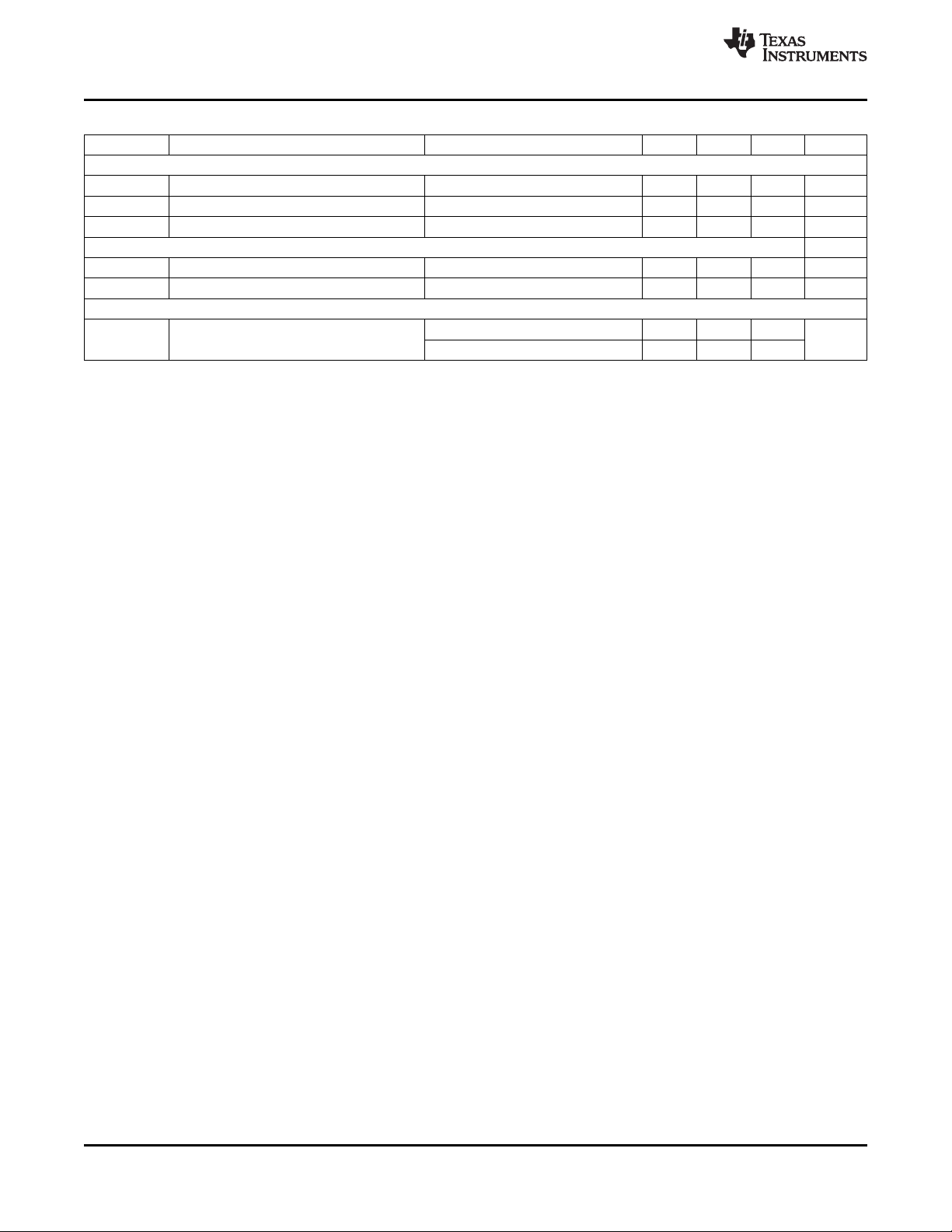
ELECTRICAL CHARACTERISTICS
LM3404
VIN= 24V unless otherwise indicated. Typicals and limits appearing in plain type apply for TA= TJ= 25°C.
in boldface type apply over full Operating Temperature Range. Datasheet min/max specification limits are specified by
design, test, or statistical analysis.
Symbol Parameter Conditions Min Typ Max Units
SYSTEM PARAMETERS
t
ON-1
t
ON-2
(1) Typical specifications represent the most likely parametric norm at 25°C operation.
On-time 1 VIN= 10V, RON= 200 kΩ 2.1 2.75 3.4 µs
On-time 2 VIN= 40V, RON= 200 kΩ 515 675 835 ns
(1)
Limits appearing
LM3404HV
Symbol Parameter Conditions Min Typ Max Units
SYSTEM PARAMETERS
t
ON-1
t
ON-2
LM3404/LM3404HV
Symbol Parameter Conditions Min Typ Max Units
REGULATION AND OVER-VOLTAGE COMPARATORS
V
REF-REG
V
REF-0V
I
CS
SHUTDOWN
V
SD-TH
V
SD-HYS
OFF TIMER
t
OFF-MIN
INTERNAL REGULATOR
V
CC-REG
V
IN-DO
V
CC-BP-TH
V
CC-BP-HYS
V
CC-Z-6
V
CC-Z-8
V
CC-Z-24
V
CC-LIM
V
CC-UV-TH
V
CC-UV-HYS
V
CC-UV-DLY
I
IN-OP
I
IN-SD
CURRENT LIMIT
I
LIM
DIM COMPARATOR
V
IH
V
IL
I
DIM-PU
On-time 1 VIN= 10V, RON= 200 kΩ 2.1 2.75 3.4 µs
On-time 2 VIN= 70V, RON= 200 kΩ 325 415 505 ns
(1)
CS Regulation Threshold CS Decreasing, SW turns on 194 200 206 mV
CS Over-voltage Threshold CS Increasing, SW turns off 300 mV
CS Bias Current CS = 0V 0.1 µA
Shutdown Threshold RON/ SD Increasing 0.3 0.7 1.05 V
Shutdown Hysteresis RON/ SD Decreasing 40 mV
Minimum Off-time CS = 0V 270 ns
VCCRegulated Output 6.4 7 7.4 V
VIN- V
CC
ICC= 5 mA, 6.0V < VIN< 8.0V 300 mV
VCCBypass Threshold VINIncreasing 8.8 V
VCCBypass Hysteresis VINDecreasing 230 mV
VIN= 6V 55
VCCOutput Impedance
(0 mA < ICC< 5 mA)
VIN= 8V 50
VIN= 24V 0.4
VCCCurrent Limit
(1)
VIN= 24V, VCC= 0V 16 mA
VCCUnder-voltage Lock-out Threshold VCCIncreasing 5.3 V
VCCUnder-voltage Lock-out Hysteresis VCCDecreasing 150 mV
VCCUnder-voltage Lock-out Filter Delay 100 mV Overdrive 3 µs
IINOperating Current Non-switching, CS = 0.5V 625 900 µA
IINShutdown Current RON / SD = 0V 95 180 µA
Current Limit Threshold 1.2 1.5 1.8 A
Logic High DIM Increasing 2.2 V
Logic Low DIM Decreasing 0.8 V
DIM Pull-up Current DIM = 1.5V 80 µA
Ω
(1) VCC provides self bias for the internal gate drive and control circuits. Device thermal limitations limit external loading.
Copyright © 2006–2013, Texas Instruments Incorporated Submit Documentation Feedback 5
Product Folder Links: LM3404 LM3404HV
Page 6
LM3404, LM3404HV
SNVS465F –OCTOBER 2006–REVISED MAY 2013
LM3404/LM3404HV
(1)
(continued)
Symbol Parameter Conditions Min Typ Max Units
MOSFET AND DRIVER
R
DS-ON
V
DR-UVLO
V
DR-HYS
Buck Switch On Resistance ISW= 200mA, BST-SW = 6.3V 0.37 0.75 Ω
BST Under-voltage Lock-out Threshold BST–SW Increasing 1.7 3 4 V
BST Under-voltage Lock-out Hysteresis BST–SW Decreasing 400 mV
THERMAL SHUTDOWN
T
SD
T
SD-HYS
Thermal Shutdown Threshold 165 °C
Thermal Shutdown Hysteresis 25 °C
THERMAL RESISTANCE
θ
JA
Junction to Ambient °C/W
SOIC-8 Package 155
So PowerPAD-8 Package
(2)
50
(2) θJAof 50°C/W with DAP soldered to a minimum of 2 square inches of 1oz. copper on the top or bottom PCB layer.
www.ti.com
6 Submit Documentation Feedback Copyright © 2006–2013, Texas Instruments Incorporated
Product Folder Links: LM3404 LM3404HV
Page 7
LM3404, LM3404HV
www.ti.com
SNVS465F –OCTOBER 2006–REVISED MAY 2013
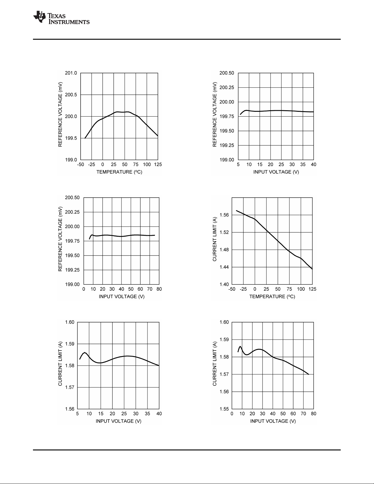
TYPICAL PERFORMANCE CHARACTERISTICS
spacer
V
vs Temperature (VIN= 24V) V
REF
Figure 3. Figure 4.
V
vs VIN, LM3404HV (TA= 25°C) Current Limit vs Temperature (VIN= 24V)
REF
vs VIN, LM3404 (TA= 25°C)
REF
Figure 5. Figure 6.
Current Limi vs VIN, LM3404 (TA= 25°C) Current Limit vs VIN, LM3404HV (TA= 25°C)
Figure 7. Figure 8.
Copyright © 2006–2013, Texas Instruments Incorporated Submit Documentation Feedback 7
Product Folder Links: LM3404 LM3404HV
Page 8
LM3404, LM3404HV
SNVS465F –OCTOBER 2006–REVISED MAY 2013
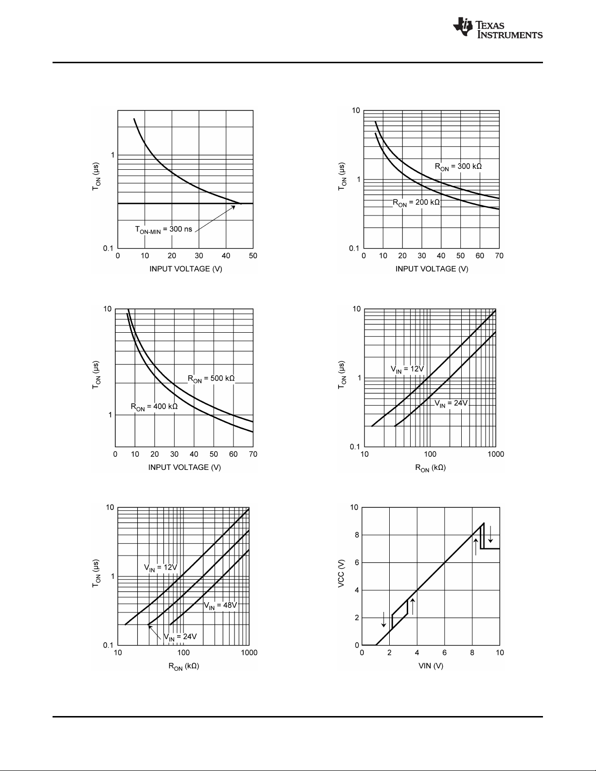
TYPICAL PERFORMANCE CHARACTERISTICS (continued)
spacer
TONvs VIN, RON= 100 kΩ (TA= 25°C) TONvs VIN, (TA= 25°C)
Figure 9. Figure 10.
TONvs VIN, (TA= 25°C) TONvs RON, LM3404 (TA= 25°C)
www.ti.com
Figure 11. Figure 12.
TONvs RON, LM3404HV (TA= 25°C) VCCvs VIN(TA= 25°C)
Figure 13. Figure 14.
8 Submit Documentation Feedback Copyright © 2006–2013, Texas Instruments Incorporated
Product Folder Links: LM3404 LM3404HV
Page 9
LM3404, LM3404HV
www.ti.com
spacer
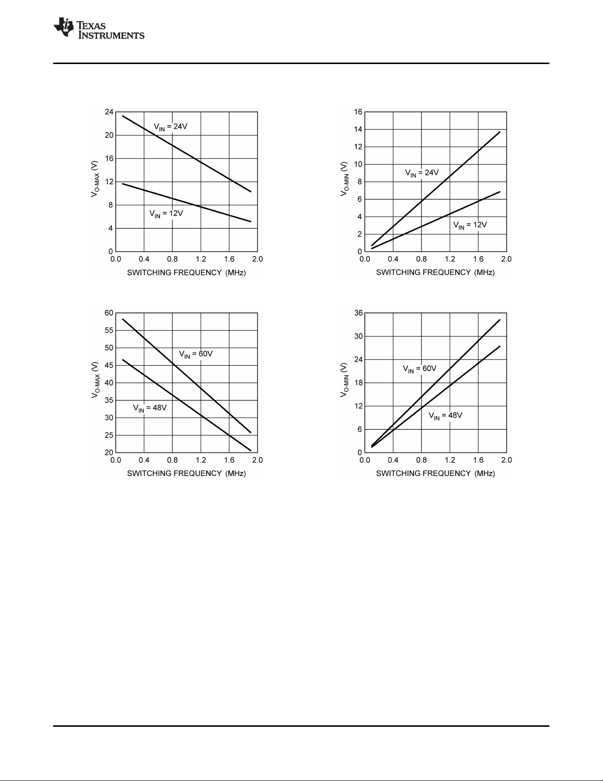
TYPICAL PERFORMANCE CHARACTERISTICS (continued)
V
vs fSW, LM3404 (TA= 25°C) V
O-MAX
Figure 15. Figure 16.
V
vs fSW, LM3404HV (TA= 25°C) V
O-MAX
SNVS465F –OCTOBER 2006–REVISED MAY 2013
vs fSW, LM3404 (TA= 25°C)
O-MIN
vs fSW, LM3404HV (TA= 25°C)
O-MIN
Figure 17. Figure 18.
Copyright © 2006–2013, Texas Instruments Incorporated Submit Documentation Feedback 9
Product Folder Links: LM3404 LM3404HV
Page 10
BOOT
VCC
VIN
SW
CS
DIM
GND
VIN
SENSE
7V BIAS
REGULATOR
BYPASS
SWITCH
VCC
UVLO
THERMAL
SHUTDOWN
ON TIMER
R
ON
Complete
Start
+
-
300 ns MIN
OFF TIMER
Complete
Start
LOGIC
+
-
+
-
+
-
CURRENT
LIMIT OFF
TIMER
BUCK
SWITCH
CURRENT
SENSE
LEVEL
SHIFT
GATE DRIVE
UVLO
VIN
+
-
1.5A
0.7V
0.2V
0.3V
1.5V
5V
75 PA
SD
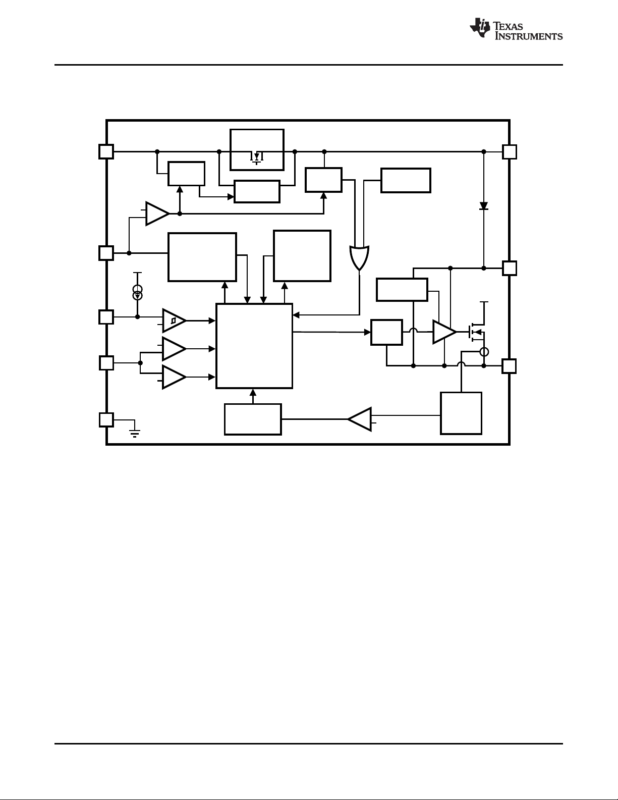
LM3404, LM3404HV
SNVS465F –OCTOBER 2006–REVISED MAY 2013
BLOCK DIAGRAM
www.ti.com
10 Submit Documentation Feedback Copyright © 2006–2013, Texas Instruments Incorporated
Product Folder Links: LM3404 LM3404HV
Page 11
f
SW
=
V
O
1.34 x 10
-10
x R
ON
VO = n x VF + 200 mV
LM3404/04HV
CS
R
SNS
One-shot
CS
Comparator
V
O
V
F
I
F
LED 1
LED n
+
-
-
+
I
F
V
SNS
V
REF
t
ON
= 1.34 x 10
-10
x
R
ON
V
LM3404, LM3404HV
www.ti.com
SNVS465F –OCTOBER 2006–REVISED MAY 2013
APPLICATION INFORMATION
THEORY OF OPERATION
The LM3404 and LM3404HV are buck regulators with a wide input voltage range, low voltage reference, and a
fast output enable/disable function. These features combine to make them ideal for use as a constant current
source for LEDs with forward currents as high as 1.2A. The controlled on-time (COT) architecture is a
combination of hysteretic mode control and a one-shot on-timer that varies inversely with input voltage.
Hysteretic operation eliminates the need for small-signal control loop compensation. When the converter runs in
continuous conduction mode (CCM) the controlled on-time maintains a constant switching frequency over the
range of input voltage. Fast transient response, PWM dimming, a low power shutdown mode, and simple output
overvoltage protection round out the functions of the LM3404/04HV.
CONTROLLED ON-TIME OVERVIEW
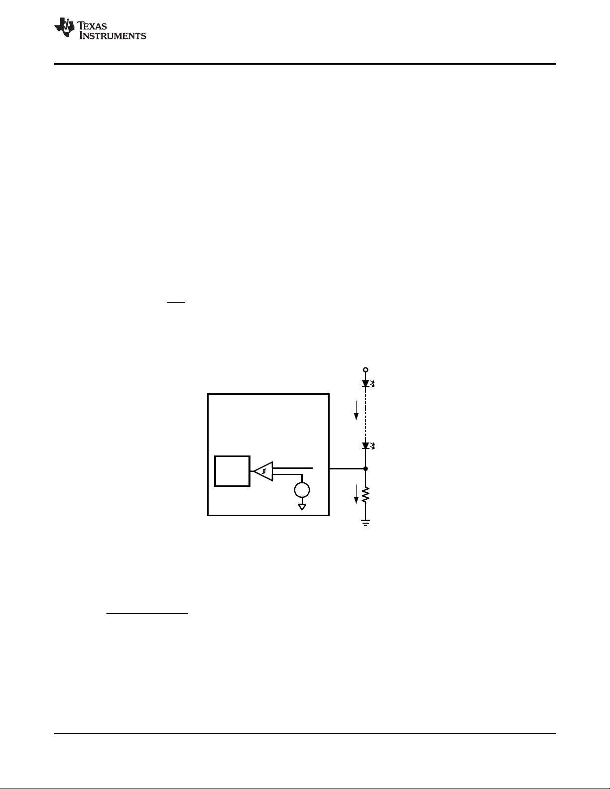
Figure 19 shows the feedback system used to control the current through an array of LEDs. A voltage signal,
V
, is created as the LED current flows through the current setting resistor, R
SNS
to the CS pin, where it is compared against a 200 mV reference, V
MOSFET when V
falls below V
SNS
. The power MOSFET conducts for a controlled on-time, tON, set by an
REF
. The on-comparator turns on the power
REF
external resistor, RON, and by the input voltage, VIN. On-time is governed by the following equation:
At the conclusion of tONthe power MOSFET turns off for a minimum off-time, t
complete the CS comparator compares V
SNS
and V
again, waiting to begin the next cycle.
REF
, to ground. V
SNS
, of 300 ns. Once t
OFF-MIN
is fed back
SNS
OFF-MIN
(1)
is
The LM3404/04HV regulators should be operated in continuous conduction mode (CCM), where inductor current
stays positive throughout the switching cycle. During steady-state CCM operation, the converter maintains a
constant switching frequency that can be selected using the following equation:
Copyright © 2006–2013, Texas Instruments Incorporated Submit Documentation Feedback 11
Figure 19. Comparator and One-Shot
• VF= forward voltage of each LED
• n = number of LEDs in series (2)
Product Folder Links: LM3404 LM3404HV
Page 12
T
SW
300 ns
V
O(MIN)
= VIN x
T
SW
TSW - 300 ns
V
O(MAX)
= VIN x
TSW = 1/f
SW
n
MAX
=
V
F(MAX)
V
O(max)
- 200 mV
D
MAX
=
t
ON
t
ON
+ t
OFF-MIN
V
O(max)
= D
MAX
x V
IN
I
L-MIN
=
0.2
R
SNS
L
-
VO x t
SNS
LM3404, LM3404HV
SNVS465F –OCTOBER 2006–REVISED MAY 2013
www.ti.com
AVERAGE LED CURRENT ACCURACY
The COT architecture regulates the valley of ΔV
current (which is also the average inductor current) the valley inductor current is calculated using the following
expression:
In this equation t
average inductor/LED current is equal to I
IF= IL= I
L-MIN
represents the propagation delay of the CS comparator, and is approximately 220 ns. The
SNS
+ ΔiL/ 2 (4)
plus one-half of the inductor current ripple, ΔiL:
L-MIN
Detailed information for the calculation of ΔiLis given in the Design Considerations section.
, the AC portion of V
SNS
. To determine the average LED
SNS
(3)
MAXIMUM OUTPUT VOLTAGE
The 300 ns minimum off-time limits the maximum duty cycle of the converter, D
output voltage, V
The maximum number of LEDs, n
maximum forward voltage of the LEDs used, V
, determined by the following equations:
O(MAX)
, that can be placed in a single series string is governed by V
MAX
F(MAX)
, using the expression:
, and in turn the maximum
MAX
O(MAX)
(5)
and the
(6)
At low switching frequency the maximum duty cycle and output voltage are higher, allowing the LM3404/04HV to
regulate output voltages that are nearly equal to input voltage. The following equation relates switching frequency
to maximum output voltage, and is also shown graphically in the Typical Performance Characteristics section:
(7)
MINIMUM OUTPUT VOLTAGE
The minimum recommended on-time for the LM3404/04HV is 300 ns. This lower limit for tONdetermines the
minimum duty cycle and output voltage that can be regulated based on input voltage and switching frequency.
The relationship is determined by the following equation, shown on the same graphs as maximum output voltage
in the Typical Performance Characteristics section:
(8)
HIGH VOLTAGE BIAS REGULATOR
The LM3404/04HV contains an internal linear regulator with a 7V output, connected between the VIN and the
VCC pins. The VCC pin should be bypassed to the GND pin with a 0.1 µF ceramic capacitor connected as close
as possible to the pins of the IC. VCC tracks VIN until VIN reaches 8.8V (typical) and then regulates at 7V as
VIN increases. Operation begins when VCC crosses 5.25V.
12 Submit Documentation Feedback Copyright © 2006–2013, Texas Instruments Incorporated
Product Folder Links: LM3404 LM3404HV
Page 13

LM3404, LM3404HV
www.ti.com
SNVS465F –OCTOBER 2006–REVISED MAY 2013
INTERNAL MOSFET AND DRIVER
The LM3404/04HV features an internal power MOSFET as well as a floating driver connected from the SW pin to
the BOOT pin. Both rise time and fall time are 20 ns each (typical) and the approximate gate charge is 6 nC. The
high-side rail for the driver circuitry uses a bootstrap circuit consisting of an internal high-voltage diode and an
external 10 nF capacitor, CB. VCCcharges CBthrough the internal diode while the power MOSFET is off. When
the MOSFET turns on, the internal diode reverse biases. This creates a floating supply equal to the VCCvoltage
minus the diode drop to drive the MOSFET when its source voltage is equal to VIN.
FAST SHUTDOWN FOR PWM DIMMING
The DIM pin of the LM3404/04HV is a TTL compatible input for low frequency PWM dimming of the LED. A logic
low (below 0.8V) at DIM will disable the internal MOSFET and shut off the current flow to the LED array. While
the DIM pin is in a logic low state the support circuitry (driver, bandgap, VCC) remains active in order to minimize
the time needed to turn the LED array back on when the DIM pin sees a logic high (above 2.2V). A 75 µA
(typical) pull-up current ensures that the LM3404/04HV is on when DIM pin is open circuited, eliminating the
need for a pull-up resistor. Dimming frequency, f
, and duty cycle, D
DIM
, are limited by the LED current rise time
DIM
and fall time and the delay from activation of the DIM pin to the response of the internal power MOSFET. In
general, f
should be at least one order of magnitude lower than the steady state switching frequency in order
DIM
to prevent aliasing.
PEAK CURRENT LIMIT
The current limit comparator of the LM3404/04HV will engage whenever the power MOSFET current (equal to
the inductor current while the MOSFET is on) exceeds 1.5A (typical). The power MOSFET is disabled for a cooldown time that is approximately 75x the steady-state on-time. At the conclusion of this cool-down time the
system re-starts. If the current limit condition persists the cycle of cool-down time and restarting will continue,
creating a low-power hiccup mode, minimizing thermal stress on the LM3404/04HV and the external circuit
components.
OVER-VOLTAGE/OVER-CURRENT COMPARATOR
The CS pin includes an output over-voltage/over-current comparator that will disable the power MOSFET
whenever V
overshoot is limited to 300 mV / R
The OVP/OCP comparator can also be used to prevent the output voltage from rising to V
an output open-circuit. This is the most common failure mode for LEDs, due to breaking of the bond wires. In a
current regulator an output open circuit causes V
shows a method using a zener diode, Z1, and zener limiting resistor, RZ, to limit output voltage to the reverse
breakdown voltage of Z1 plus 200 mV. The zener diode reverse breakdown voltage, VZ, must be greater than the
maximum combined VFof all LEDs in the array. The maximum recommended value for RZis 1 kΩ.
As discussed in the Maximum Output Voltage section, there is a limit to how high VOcan rise during an output
open-circuit that is always less than VIN. If no output capacitor is used, the output stage of the LM3404/04HV is
capable of withstanding V
and can go above VINor below 0V. A small (typically 10 nF) capacitor across the LED array dampens this
oscillation. For circuits that use an output capacitor, the system can still withstand V
COis rated to handle VIN. The high current paths are blocked in output open-circuit and the risk of thermal stress
is minimal, hence the user may opt to allow the output voltage to rise in the case of an open-circuit LED failure.
exceeds 300 mV. This threshold provides a hard limit for the output current. Output current
SNS
O(MAX)
by this comparator during transients.
SNS
in the event of
O(MAX)
to fall to zero, commanding maximum duty cycle. Figure 20
SNS
indefinitely, however the voltage at the output end of the inductor will oscillate
indefinitely as long as
O(MAX)
Copyright © 2006–2013, Texas Instruments Incorporated Submit Documentation Feedback 13
Product Folder Links: LM3404 LM3404HV
Page 14

ON/OFF
Q1
2N7000 or
equivalent
GND
DIM
BOOT SW
CS
RON
LM3404/04HV
VIN
D1
L1
C
B
R
SNS
C
F
R
ON
C
IN
V
IN
I
F
VCC
GND
DIM
BOOT SW
CS
RON
LM3404/04HV
VIN
D1
L1
C
B
R
SNS
C
F
R
ON
C
IN
V
IN
VCC
R
Z
Z1
LM3404, LM3404HV
SNVS465F –OCTOBER 2006–REVISED MAY 2013
www.ti.com
Figure 20. Output Open Circuit Protection
LOW POWER SHUTDOWN
The LM3404/04HV can be placed into a low power state (I
level MOSFET as shown in Figure 21. Low power MOSFETs like the 2N7000, 2N3904, or equivalent are
recommended devices for putting the LM3404/04HV into low power shutdown. Logic gates can also be used to
shut down the LM3404/04HV as long as the logic low voltage is below the over temperature minimum threshold
of 0.3V. Noise filter circuitry on the RON pin can cause a few pulses with longer on-times than normal after RON
is grounded or released. In these cases the OVP/OCP comparator will ensure that the peak inductor or LED
current does not exceed 300 mV / R
SNS
.
= 90 µA) by grounding the RON pin with a signal-
IN-SD
Figure 21. Low Power Shutdown
THERMAL SHUTDOWN
Internal thermal shutdown circuitry is provided to protect the IC in the event that the maximum junction
temperature is exceeded. The threshold for thermal shutdown is 165°C with a 25°C hysteresis (both values
typical). During thermal shutdown the MOSFET and driver are disabled.
14 Submit Documentation Feedback Copyright © 2006–2013, Texas Instruments Incorporated
Product Folder Links: LM3404 LM3404HV
Page 15

L
VIN - V
O
'iL = 'iF =
t
ON
LM3404, LM3404HV
www.ti.com
SNVS465F –OCTOBER 2006–REVISED MAY 2013
DESIGN CONSIDERATIONS
SWITCHING FREQUENCY
Switching frequency is selected based on the trade-offs between efficiency (better at low frequency), solution
size/cost (smaller at high frequency), and the range of output voltage that can be regulated (wider at lower
frequency.) Many applications place limits on switching frequency due to EMI sensitivity. The on-time of the
LM3404/04HV can be programmed for switching frequencies ranging from the 10’s of kHz to over 1 MHz. The
maximum switching frequency is limited only by the minimum on-time and minimum off-time requirements.
LED RIPPLE CURRENT
Selection of the ripple current, ΔiF, through the LED array is analogous to the selection of output ripple voltage in
a standard voltage regulator. Where the output ripple in a voltage regulator is commonly ±1% to ±5% of the DC
output voltage, LED manufacturers generally recommend values for ΔiFranging from ±5% to ±20% of IF. Higher
LED ripple current allows the use of smaller inductors, smaller output capacitors, or no output capacitors at all.
The advantages of higher ripple current are reduction in the solution size and cost. Lower ripple current requires
more output inductance, higher switching frequency, or additional output capacitance. The advantages of lower
ripple current are a reduction in heating in the LED itself and greater tolerance in the average LED current before
the current limit of the LED or the driving circuitry is reached.
BUCK CONVERTERS WITHOUT OUTPUT CAPACITORS
The buck converter is unique among non-isolated topologies because of the direct connection of the inductor to
the load during the entire switching cycle. By definition an inductor will control the rate of change of current that
flows through it, and this control over current ripple forms the basis for component selection in both voltage
regulators and current regulators. A current regulator such as the LED driver for which the LM3404/04HV was
designed focuses on the control of the current through the load, not the voltage across it. A constant current
regulator is free of load current transients, and has no need of output capacitance to supply the load and
maintain output voltage. Referring to the Typical Application circuit on the front page of this datasheet, the
inductor and LED can form a single series chain, sharing the same current. When no output capacitor is used,
the same equations that govern inductor ripple current, ΔiL, also apply to the LED ripple current, ΔiF. For a
controlled on-time converter such as LM3404/04HV the ripple current is described by the following expression:
A minimum ripple voltage of 25 mV is recommended at the CS pin to provide good signal to noise ratio (SNR).
The CS pin ripple voltage, Δv
BUCK CONVERTERS WITH OUTPUT CAPACITORS
A capacitor placed in parallel with the LED or array of LEDs can be used to reduce the LED current ripple while
keeping the same average current through both the inductor and the LED array. This technique is demonstrated
in Design Examples 1 and 2. With this topology the output inductance can be lowered, making the magnetics
smaller and less expensive. Alternatively, the circuit could be run at lower frequency but keep the same inductor
value, improving the efficiency and expanding the range of output voltage that can be regulated. Both the peak
current limit and the OVP/OCP comparator still monitor peak inductor current, placing a limit on how large Δi
can be even if ΔiFis made very small. A parallel output capacitor is also useful in applications where the inductor
or input voltage tolerance is poor. Adding a capacitor that reduces ΔiFto well below the target provides
headroom for changes in inductance or VINthat might otherwise push the peak LED ripple current too high.
Figure 22 shows the equivalent impedances presented to the inductor current ripple when an output capacitor,
CO, and its equivalent series resistance (ESR) are placed in parallel with the LED array. The entire inductor
ripple current flows through R
comparator.
Copyright © 2006–2013, Texas Instruments Incorporated Submit Documentation Feedback 15
Δv
SNS
= ΔiFx R
SNS
, is described by the following:
SNS
to provide the required 25 mV of ripple voltage for proper operation of the CS
SNS
Product Folder Links: LM3404 LM3404HV
(9)
(10)
L
Page 16

C
IN (MIN)
=
'V
IN (MAX)
IF x t
ON
'iF =
Z
C
= ESR +
'i
L
r
D
1 +
Z
C
1
2Sx f
SW
x C
O
'i
L
ESR
r
D
R
SNS
'i
C
'
i
F
'i
L
C
O
LM3404, LM3404HV
SNVS465F –OCTOBER 2006–REVISED MAY 2013
www.ti.com
Figure 22. LED and CORipple Current
To calculate the respective ripple currents the LED array is represented as a dynamic resistance, rD. LED
dynamic resistance is not always specified on the manufacturer’s datasheet, but it can be calculated as the
inverse slope of the LED’s VFvs. IFcurve. Note that dividing VFby IFwill give an incorrect value that is 5x to 10x
too high. Total dynamic resistance for a string of n LEDs connected in series can be calculated as the rDof one
device multiplied by n. Inductor ripple current is still calculated with the expression from Buck Regulators without
Output Capacitors. The following equations can then be used to estimate ΔiFwhen using a parallel capacitor:
(11)
The calculation for ZCassumes that the shape of the inductor ripple current is approximately sinusoidal.
Small values of COthat do not significantly reduce ΔiFcan also be used to control EMI generated by the
switching action of the LM3404/04HV. EMI reduction becomes more important as the length of the connections
between the LED and the rest of the circuit increase.
INPUT CAPACITORS
Input capacitors at the VIN pin of the LM3404/04HV are selected using requirements for minimum capacitance
and rms ripple current. The input capacitors supply pulses of current approximately equal to IFwhile the power
MOSFET is on, and are charged up by the input voltage while the power MOSFET is off. Switching converters
such as the LM3404/04HV have a negative input impedance due to the decrease in input current as input
voltage increases. This inverse proportionality of input current to input voltage can cause oscillations (sometimes
called ‘power supply interaction’) if the magnitude of the negative input impedance is greater the the input filter
impedance. Minimum capacitance can be selected by comparing the input impedance to the converter’s negative
resistance; however this requires accurate calculation of the input voltage source inductance and resistance,
quantities which can be difficult to determine. An alternative method to select the minimum input capacitance,
C
the change in voltage across CINduring the converter on-time, when CINsupplies the load current. C
be selected with the following:
16 Submit Documentation Feedback Copyright © 2006–2013, Texas Instruments Incorporated
, is to select the maximum input voltage ripple which can be tolerated. This value, Δv
IN(MIN)
Product Folder Links: LM3404 LM3404HV
IN(MAX)
, is equal to
can
IN(MIN)
(12)
Page 17

I
IN(rms)
= IF x
D(1 - D)
LM3404, LM3404HV
www.ti.com
SNVS465F –OCTOBER 2006–REVISED MAY 2013
A good starting point for selection of CINis to use an input voltage ripple of 5% to 10% of VIN. A minimum input
capacitance of 2x the C
value is recommended for all LM3404/04HV circuits. To determine the rms current
IN(MIN)
rating, the following formula can be used:
(13)
Ceramic capacitors are the best choice for the input to the LM3404/04HV due to their high ripple current rating,
low ESR, low cost, and small size compared to other types. When selecting a ceramic capacitor, special
attention must be paid to the operating conditions of the application. Ceramic capacitors can lose one-half or
more of their capacitance at their rated DC voltage bias and also lose capacitance with extremes in temperature.
A DC voltage rating equal to twice the expected maximum input voltage is recommended. In addition, the
minimum quality dielectric which is suitable for switching power supply inputs is X5R, while X7R or better is
preferred.
RECIRCULATING DIODE
The LM3404/04HV is a non-synchronous buck regulator that requires a recirculating diode D1 (see the Typical
Application circuit) to carrying the inductor current during the MOSFET off-time. The most efficient choice for D1
is a Schottky diode due to low forward drop and near-zero reverse recovery time. D1 must be rated to handle the
maximum input voltage plus any switching node ringing when the MOSFET is on. In practice all switching
converters have some ringing at the switching node due to the diode parasitic capacitance and the lead
inductance. D1 must also be rated to handle the average current, ID, calculated as:
ID= (1 – D) x I
F
This calculation should be done at the maximum expected input voltage. The overall converter efficiency
becomes more dependent on the selection of D1 at low duty cycles, where the recirculating diode carries the
load current for an increasing percentage of the time. This power dissipation can be calculating by checking the
typical diode forward voltage, VD, from the I-V curve on the product datasheet and then multiplying it by ID. Diode
datasheets will also provide a typical junction-to-ambient thermal resistance, θJA, which can be used to estimate
the operating die temperature of the device. Multiplying the power dissipation (PD= IDx VD) by θJAgives the
temperature rise. The diode case size can then be selected to maintain the Schottky diode temperature below
the operational maximum.
(14)
LED CURRENT DURING DIM MODE
The LM3402 contains high speed MOSFET gate drive circuitry that switches the main internal power MOSFET
between “on” and “off” states. This circuitry uses current derived from the VCC regulator to charge the MOSFET
during turn-on, then dumps current from the MOSFET gate to the source (the SW pin) during turn-off. As shown
in the block diagram, the MOSFET drive circuitry contains a gate drive under-voltage lockout (UVLO) circuit that
ensures the MOSFET remains off when there is inadequate VCC voltage for proper operation of the driver. This
watchdog circuitry is always running including during DIM and shutdown modes, and supplies a small amount of
current from VCC to SW. Because the SW pin is connected directly to the LEDs through the buck inductor, this
current returns to ground through the LEDs. The amount of current sourced is a function of the SW voltage, as
shown in Figure 23.
Copyright © 2006–2013, Texas Instruments Incorporated Submit Documentation Feedback 17
Product Folder Links: LM3404 LM3404HV
Page 18
0
5
10
15
20
25
0 1 2 3 4 5 6
SW VOLTAGE (V)
SW CURRENT (PA)
LM3404, LM3404HV
SNVS465F –OCTOBER 2006–REVISED MAY 2013
www.ti.com
Figure 23. LED Current From SW Pin
Though most power LEDs are designed to run at several hundred milliamps, some can be seen to glow with a
faint light at extremely low current levels, as low as a couple microamps in some instances. In lab testing, the
forward voltage was found to be approximately 2V for LEDs that exhibited visible light at these low current levels.
For LEDs that did not show light emission at very low current levels, the forward voltage was found to be around
900mV. It is important to remember that the forward voltage is also temperature dependent, decreasing at higher
temperatures. Consequently, with a maximum Vcc voltage of 7.4V, current will be observed in the LEDs if the
total stack voltage is less than about 6V at a forward current of several microamps. No current is observed if the
stack voltage is above 6V, as shown in Figure 23. The need for absolute darkness during DIM mode is also
application dependent. It will not affect regular PWM dimming operation.
The fix for this issue is extremely simple. Place a resistor from the SW pin to ground according to the chart
below.
The luminaire designer should ensure that the suggested resistor is effective in eliminating the off-state light
output. A combination of calculations based on LED manufacturer data and lab measurements over temperature
will ensure the best design.
TRANSIENT PROTECTION CONSIDERATIONS
Considerations need to be made when external sources, loads or connections are made to the switching
converter circuit due to the possibility of Electrostatic Discharge (ESD) or Electric Over Stress (EOS) events
occurring and damaging the integrated circuit (IC) device. All IC device pins contain zener based clamping
structures that are meant to clamp ESD. ESD events are very low energy events, typically less than 5µJ
(microjoules). Any event that transfers more energy than this may damage the ESD structure. Damage is
typically represented as a short from the pin to ground as the extreme localized heat of the ESD / EOS event
causes the aluminum metal on the chip to melt, causing the short. This situation is common to all integrated
circuits and not just unique to the LM340X device.
18 Submit Documentation Feedback Copyright © 2006–2013, Texas Instruments Incorporated
Number of LEDs Resistor Value (kΩ)
1 20
2 50
3 90
4 150
5 200
>5 300
Product Folder Links: LM3404 LM3404HV
Page 19

SW
LM3404
GND
CS
8V
V
TRANSIENT
~ 0.675
Module
Connector
Module
Connector
LM3404, LM3404HV
www.ti.com
SNVS465F –OCTOBER 2006–REVISED MAY 2013
CS PIN PROTECTION
When hot swapping in a load (e.g. test points, load boards, LED stack), any residual charge on the load will be
immediately transferred through the output capacitor to the CS pin, which is then damaged as shown in
Figure 24 below. The EOS event due to the residual charge from the load is represented as V
TRANSIENT
.
From measurements, we know that the 8V ESD structure on the CS pin can typically withstand 25mA of direct
current (DC). Adding a 1kΩ resistor in series with the CS pin, shown in Figure 25, results in the majority of the
transient energy to pass through the discrete sense resistor rather than the device. The series resistor limits the
peak current that can flow during a transient event, thus protecting the CS pin. With the 1kΩ resistor shown, a
33V, 49A transient on the LED return connector terminal could be absorbed as calculated by:
V = 25mA * 1kΩ + 8V = 33V (15)
I = 33V / 0.67Ω = 49A (16)
This is an extremely high energy event, so the protection measures previously described should be adequate to
solve this issue.
Figure 24. CS Pin, Transient Path
Copyright © 2006–2013, Texas Instruments Incorporated Submit Documentation Feedback 19
Product Folder Links: LM3404 LM3404HV
Page 20

SW
LM3404
GND
CS
8V
V
TRANSIENT
~ 0.675
Module
Connector
Module
Connector
1 k5
LM3404, LM3404HV
SNVS465F –OCTOBER 2006–REVISED MAY 2013
www.ti.com
Figure 25. CS Pin, Transient Path with Protection
Adding a resistor in series with the CS pin causes the observed output LED current to shift very slightly. The
reason for this is twofold: (1) the CS pin has about 20pF of inherent capacitance inside it which causes a slight
delay (20ns for a 1kΩ series resistor), and (2) the comparator that is watching the voltage at the CS pin uses a
pnp bipolar transistor at its input. The base current of this pnp transistor is approximately 100nA which will cause
a 0.1mV change in the 200mV threshold. These are both very minor changes and are well understood. The shift
in current can either be neglected or taken into consideration by changing the current sense resistance slightly.
CS PIN PROTECTION WITH OVP
When designing output overvoltage protection into the switching converter circuit using a zener diode, transient
protection on the CS pin requires additional consideration. As shown in Figure 26, adding a zener diode from the
output to the CS pin (with the series resistor) for output overvoltage protection will now again allow the transient
energy to be passed
Adding an additional series resistor to the CS pin as shown in Figure 27 will result in the majority of the transient
energy to pass through the sense resistor thereby protecting the LM340X device.
20 Submit Documentation Feedback Copyright © 2006–2013, Texas Instruments Incorporated
Product Folder Links: LM3404 LM3404HV
Page 21

SW
LM3404
GND
CS
8V
V
TRANSIENT
~ 0.675
Module
Connector
Module
Connector
50051 k5
SW
LM3404
GND
CS
8V
V
TRANSIENT
~ 0.675
Module
Connector
Module
Connector
1 k5
LM3404, LM3404HV
www.ti.com
SNVS465F –OCTOBER 2006–REVISED MAY 2013
Figure 26. CS Pin with OVP, Transient Path
Figure 27. CS Pin with OVP, Transient Path with Protection
Copyright © 2006–2013, Texas Instruments Incorporated Submit Documentation Feedback 21
Product Folder Links: LM3404 LM3404HV
Page 22

VIN
LM3404
GND
80V
V
IN
Module
Connector
Module
Connector
TVS
C
IN
Board Trace
Inductance
LM3404, LM3404HV
SNVS465F –OCTOBER 2006–REVISED MAY 2013
www.ti.com
VIN PIN PROTECTION
The VIN pin also has an ESD structure from the pin to GND with a breakdown voltage of approximately 80V. Any
transient that exceeds this voltage may damage the device. Although transient absorption is usually present at
the front end of a switching converter circuit, damage to the VIN pin can still occur.
When VINis hot swapped in, the current that rushes in to charge CINup to the VINvalue also charges (energizes)
the circuit board trace inductance as shown in Figure 28. The excited trace inductance then resonates with the
input capacitance (similar to an under-damped LC tank circuit) and causes voltages at the VIN pin to rise well in
excess of both VINand the voltage at the module input connector as clamped by the input TVS. If the resonating
voltage at the VIN pin exceeds the 80V breakdown voltage of the ESD structure, the ESD structure will activate
and then “snap-back” to a lower voltage due to its inherent design. If this lower snap-back voltage is less than
the applied nominal VINvoltage, then significant current will flow through the ESD structure resulting in the IC
being damaged.
An additional TVS or small zener diode should be placed as close as possible to the VIN pins of each IC on the
board, in parallel with the input capacitor as shown in Figure 29. A minor amount of series resistance in the input
line would also help, but would lower overall conversion efficiency. For this reason, NTC resistors are often used
as inrush limiters instead.
22 Submit Documentation Feedback Copyright © 2006–2013, Texas Instruments Incorporated
Figure 28. VIN Pin with Typical Input Protection
Product Folder Links: LM3404 LM3404HV
Page 23

VIN
LM3404
GND
80V
V
IN
Module
Connector
Module
Connector
TVS
C
IN
Board Trace
Inductance
TVS or
smaller
zener diode
LM3404, LM3404HV
www.ti.com
SNVS465F –OCTOBER 2006–REVISED MAY 2013
Figure 29. VIN Pin with Additional Input Protection
GENERAL COMMENTS REGARDING OTHER PINS
Any pin that goes “off-board” through a connector should have series resistance of at least 1kΩ to 10kΩ in series
with it to protect it from ESD or other transients. These series resistors limit the peak current that can flow (or
cause a voltage drop) during a transient event, thus protecting the pin and the device. Pins that are not used
should not be left floating. They should instead be tied to GND or to an appropriate voltage through resistance.
Design Example 1: LM3404
The first example circuit will guide the user through component selection for an architectural accent lighting
application. A regulated DC voltage input of 24V ±10% will power a 5.4W "warm white" LED module that consists
of four LEDs in a 2 x 2 series-parallel configuration. The module will be treated as a two-terminal element and
driven with a forward current of 700 mA ±5%. The typical forward voltage of the LED module in thermal steady
state is 6.9V, hence the average output voltage will be 7.1V. The objective of this application is to place the
complete current regulator and LED module in a compact space formerly occupied by a halogen light source.
(The LED will be on a separate metal-core PCB and heatsink.) Switching frequency will be 400 kHz to keep
switching loss low, as the confined space with no air-flow requires a maximum temperature rise of 50°C in each
circuit component. A small solution size is also important, as the regulator must fit on a circular PCB with a 1.5"
diameter. A complete bill of materials can be found in Table 1 at the end of this datasheet.
Copyright © 2006–2013, Texas Instruments Incorporated Submit Documentation Feedback 23
Product Folder Links: LM3404 LM3404HV
Page 24

L
MIN
=
VIN - V
O
'i
L
x t
ON
R
ON
=
V
O
1.34 x 10
-10
x f
SW
GND
DIM
BOOT SW
CS
RON
LM3404
VIN
D1
L1
C
B
R
SNS
C
F
R
ON
C
IN
VIN = 24V
IF = 700 mA
VCC
C
O
LED1
LM3404, LM3404HV
SNVS465F –OCTOBER 2006–REVISED MAY 2013
www.ti.com
Figure 30. Schematic for Design Example 1
RONand t
ON
A moderate switching frequency is needed in this application to balance the requirements of magnetics size and
efficiency. RONis selected from the equation for switching frequency as follows:
RON= 7.1 / (1.34 x 10
-10
x 4 x 105) = 132.5 kΩ (18)
The closest 1% tolerance resistor is 133 kΩ. The switching frequency and on-time of the circuit can then be
found using the equations relating RONand tONto fSW:
fSW= 7.1 / (1.33 x 105x 1.34 x 10
tON= (1.34 x 10
-10
x 1.33 x 105) / 24 = 743 ns (20)
-10
) = 398 kHz (19)
OUTPUT INDUCTOR
Since an output capacitor will be used to filter some of the AC ripple current, the inductor ripple current can be
set higher than the LED ripple current. A value of 40%
ΔiL= 0.4 x 0.7 = 0.28A (21)
is typical in many buck converters:
P-P
With the target ripple current determined the inductance can be chosen:
L
= [(24 – 7.1) x 7.43 x 10-7] / (0.28) = 44.8 µH (23)
MIN
The closest standard inductor value is 47 µH. The average current rating should be greater than 700 mA to
prevent overheating in the inductor. Separation between the LM3404 drivers and the LED arrays means that heat
from the inductor will not threaten the lifetime of the LEDs, but an overheated inductor could still cause the
LM3404 to enter thermal shutdown.
The inductance of the standard part chosen is ±20%. With this tolerance the typical, minimum, and maximum
inductor current ripples can be calculated:
Δi
= [(24 - 7.1) x 7.43 x 10-7] / 47 x 10-6= 266 mA
L(TYP)
Δi
= [(24 - 7.1) x 7.43 x 10-7] / 56 x 10-6= 223 mA
L(MIN)
Δi
= [(24 - 7.1) x 7.43 x 10-7] / 38 x 10-6= 330 mA
L(MAX)
P-P
P-P
P-P
(17)
(22)
(24)
(25)
(26)
24 Submit Documentation Feedback Copyright © 2006–2013, Texas Instruments Incorporated
Product Folder Links: LM3404 LM3404HV
Page 25

R
SNS
=
2
VIN - V
O
0.2 x L
IF x L + VO x t
SNS
-
x t
ON
'i
F
x r
D
'iL - 'i
F
ZC =
LM3404, LM3404HV
www.ti.com
SNVS465F –OCTOBER 2006–REVISED MAY 2013
The peak LED/inductor current is then estimated:
I
= IL+ 0.5 x Δi
L(PEAK)
I
= 0.7 + 0.5 x 0.330 = 866 mA (28)
L(PEAK)
L(MAX)
(27)
In the case of a short circuit across the LED array, the LM3404 will continue to deliver rated current through the
short but will reduce the output voltage to equal the CS pin voltage of 200 mV. The inductor ripple current and
peak current in this condition would be equal to:
Δi
L(LED-SHORT)
I
L(PEAK)
= [(24 – 0.2) x 7.43 x 10-7] / 38 x 10-6= 465 mA
P-P
(29)
= 0.7 + 0.5 x 0.465 = 933 mA (30)
In the case of a short at the switch node, the output, or from the CS pin to ground the short circuit current limit
will engage at a typical peak current of 1.5A. In order to prevent inductor saturation during these fault conditions
the inductor’s peak current rating must be above 1.5A. A 47 µH off-the shelf inductor rated to 1.4A (peak) and
1.5A (average) with a DCR of 0.1Ω will be used.
USING AN OUTPUT CAPACITOR
This application does not require high frequency PWM dimming, allowing the use of an output capacitor to
reduce the size and cost of the output inductor. To select the proper output capacitor the equation from Buck
Regulators with Output Capacitors is re-arranged to yield the following:
(31)
The target tolerance for LED ripple current is 100 mA
, and a typical value for rDof 1.8Ω at 700 mA can be read
P-P
from the LED datasheet. The required capacitor impedance to reduce the worst-case inductor ripple current of
333 mA
is therefore:
P-P
ZC= [0.1 / (0.333 - 0.1] x 1.8 = 0.77Ω (32)
A ceramic capacitor will be used and the required capacitance is selected based on the impedance at 400 kHz:
CO= 1/(2 x π x 0.77 x 4 x 105) = 0.51 µF (33)
This calculation assumes that impedance due to the equivalent series resistance (ESR) and equivalent series
inductance (ESL) of COis negligible. The closest 10% tolerance capacitor value is 1.0 µF. The capacitor used
should be rated to 25V or more and have an X7R dielectric. Several manufacturers produce ceramic capacitors
with these specifications in the 0805 case size. A typical value for ESR of 3 mΩ can be read from the curve of
impedance vs. frequency in the product datasheet.
R
SNS
A preliminary value for R
was determined in selecting ΔiL. This value should be re-evaluated based on the
SNS
calculations for ΔiF:
t
= 220 ns, R
SNS
= 0.33Ω (35)
SNS
Sub-1Ω resistors are available in both 1% and 5% tolerance. A 1%, 0.33Ω device is the closest value, and a
0.33W, 1206 size device will handle the power dissipation of 162 mW. With the resistance selected, the average
value of LED current is re-calculated to ensure that current is within the ±5% tolerance requirement. From the
expression for average LED current:
IF= 0.2 / 0.33 - (7.1 x 2.2 x 10-7) / 47 x 10-6+ 0.266 / 2 (36)
= 706 mA, 1% above 700 mA (37)
INPUT CAPACITOR
Following the calculations from the Input Capacitor section, Δv
IN(MAX)
will be 24V x 2%
= 480 mV. The
P-P
minimum required capacitance is:
C
= (0.7 x 7.4 x 10-7) / 0.48 = 1.1 µF (38)
IN(MIN)
Copyright © 2006–2013, Texas Instruments Incorporated Submit Documentation Feedback 25
Product Folder Links: LM3404 LM3404HV
(34)
Page 26

LM3404, LM3404HV
SNVS465F –OCTOBER 2006–REVISED MAY 2013
www.ti.com
To provide additional safety margin the a higher value of 3.3 µF ceramic capacitor rated to 50V with X7R
dielectric in an 1210 case size will be used. From the Design Considerations section, input rms current is:
I
= 0.7 x Sqrt(0.28 x 0.72) = 314 mA (39)
IN-RMS
Ripple current ratings for 1210 size ceramic capacitors are typically higher than 2A, more than enough for this
design.
RECIRCULATING DIODE
The input voltage of 24V ±5% requires Schottky diodes with a reverse voltage rating greater than 30V. The next
highest standard voltage rating is 40V. Selecting a 40V rated diode provides a large safety margin for the ringing
of the switch node and also makes cross-referencing of diodes from different vendors easier.
The next parameters to be determined are the forward current rating and case size. In this example the low duty
cycle (D = 7.1 / 24 = 28%) places a greater thermal stress on D1 than on the internal power MOSFET of the
LM3404. The estimated average diode current is:
ID= 0.706 x 0.72 = 509 mA (40)
A Schottky with a forward current rating of 1A would be adequate, however reducing the power dissipation is
critical in this example. Higher current diodes have lower forward voltages, hence a 2A-rated diode will be used.
To determine the proper case size, the dissipation and temperature rise in D1 can be calculated as shown in the
Design Considerations section. VDfor a case size such as SMB in a 40V, 2A Schottky diode at 700 mA is
approximately 0.3V and the θJAis 75°C/W. Power dissipation and temperature rise can be calculated as:
PD= 0.509 x 0.3 = 153 mW (41)
T
= 0.153 x 75 = 11.5°C (42)
RISE
CBAND C
F
The bootstrap capacitor CBshould always be a 10 nF ceramic capacitor with X7R dielectric. A 25V rating is
appropriate for all application circuits. The linear regulator filter capacitor CFshould always be a 100 nF ceramic
capacitor, also with X7R dielectric and a 25V rating.
EFFICIENCY
To estimate the electrical efficiency of this example the power dissipation in each current carrying element can
be calculated and summed. Electrical efficiency, η, should not be confused with the optical efficacy of the circuit,
which depends upon the LEDs themselves.
Total output power, PO, is calculated as:
PO= IFx VO= 0.706 x 7.1 = 5W (43)
Conduction loss, PC, in the internal MOSFET:
2
PC= (I
x R
F
) x D = (0.7062x 0.8) x 0.28 = 112 mW (44)
DSON
Gate charging and VCC loss, PG, in the gate drive and linear regulator:
PG= (I
+ fSWx QG) x VINPG= (600 x 10-6+ 4 x 105x 6 x 10-9) x 24 = 72 mW (45)
IN-OP
Switching loss, PS, in the internal MOSFET:
PS= 0.5 x VINx IFx (tR+ tF) x fSWPS= 0.5 x 24 x 0.706 x 40 x 10-9x 4 x 105= 136 mW (46)
AC rms current loss, P
P
= I
CIN
2
x ESR = 0.31720.003 = 0.3 mW (negligible) (47)
IN(rms)
, in the input capacitor:
CIN
DCR loss, PL, in the inductor
2
PL= I
x DCR = 0.7062x 0.1 = 50 mW (48)
F
Recirculating diode loss, PD= 153 mW
Current Sense Resistor Loss, P
= 164 mW
SNS
Electrical efficiency, η = PO/ (PO+ Sum of all loss terms) = 5 / (5 + 0.687) = 88%
Temperature Rise in the LM3404 IC is calculated as:
T
= (PC+ PG+ PS) x θJA= (0.112 + 0.072 + 0.136) x 155 = 49.2°C (49)
LM3404
26 Submit Documentation Feedback Copyright © 2006–2013, Texas Instruments Incorporated
Product Folder Links: LM3404 LM3404HV
Page 27

L
MIN
=
VIN - V
O
'i
L
x t
ON
R
ON
=
V
O
1.34 x 10
-10
x f
SW
GND
BOOT SW
CS
RON
LM3404HV
VIN
D1
L1
C
B
R
SNS
C
F
R
ON
C
IN
VIN = 48V ±10%
IF = 0.5A
VCC
C
O
LED1
LED10
LM3404, LM3404HV
www.ti.com
SNVS465F –OCTOBER 2006–REVISED MAY 2013
Design Example 2: LM3404HV
The second example circuit will guide the user through component selection for an outdoor general lighting
application. A regulated DC voltage input of 48V ±10% will power ten series-connected LEDs at 500 mA ±10%
with a ripple current of 50 mA
35V, hence the average output voltage will be 35.2V. A complete bill of materials can be found in Table 2 at the
end of this datasheet.
or less. The typical forward voltage of the LED module in thermal steady state is
P-P
Figure 31. Schematic for Design Example 2
RONand t
ON
A low switching frequency, 225 kHz, is needed in this application, as high efficiency and low power dissipation
take precedence over the solution size. RONis selected from the equation for switching frequency as follows:
RON= 35.2 / (1.34 x 10
-10
x 2.25 x 105) = 1.16 MΩ (51)
The next highest 1% tolerance resistor is 1.18 MΩ. The switching frequency and on-time of the circuit can then
be found using the equations relating RONand tONto fSW:
fSW= 35.2 / (1.18 x 106x 1.34 x 10
tON= (1.34 x 10
-10
x 1.18 x 106) / 48 = 3.3 µs (53)
-10
) = 223 kHz (52)
OUTPUT INDUCTOR
Since an output capacitor will be used to filter some of the AC ripple current, the inductor ripple current can be
set higher than the LED ripple current. A value of 30%
makes a good trade-off between the current ripple and
P-P
the size of the inductor:
ΔiL= 0.3 x 0.5 = 0.15A (54)
With the target ripple current determined the inductance can be chosen:
L
= [(48 – 35.2) x 3.3 x 10-6] / (0.15) = 281 µH (56)
MIN
(50)
(55)
Copyright © 2006–2013, Texas Instruments Incorporated Submit Documentation Feedback 27
Product Folder Links: LM3404 LM3404HV
Page 28

'i
F
x r
D
'iL - 'i
F
ZC =
LM3404, LM3404HV
SNVS465F –OCTOBER 2006–REVISED MAY 2013
www.ti.com
The closest standard inductor value above 281 is 330 µH. The average current rating should be greater than
0.5A to prevent overheating in the inductor. In this example the LM3404HV driver and the LED array share the
same metal-core PCB, meaning that heat from the inductor could threaten the lifetime of the LEDs. For this
reason the average current rating of the inductor used should have a de-rating of about 50%, or 1A.
The inductance of the standard part chosen is ±20%. With this tolerance the typical, minimum, and maximum
inductor current ripples can be calculated:
Δi
= [(48 - 35.2) x 3.3 x 10-6] / 330 x 10-6= 128 mA
L(TYP)
Δi
= [(48 - 35.2) x 3.3 x 10-6] / 396 x 10-6= 107 mA
L(MIN)
Δi
= [(48 - 35.2) x 3.3 x 10-6] / 264 x 10-6= 160 mA
L(MAX)
P-P
P-P
P-P
(57)
(58)
(59)
The peak inductor current is then estimated:
I
= IL+ 0.5 x Δi
L(PEAK)
I
= 0.5 + 0.5 x 0.16 = 0.58A (61)
L(PEAK)
L(MAX)
(60)
In the case of a short circuit across the LED array, the LM3404HV will continue to deliver rated current through
the short but will reduce the output voltage to equal the CS pin voltage of 200 mV. The inductor ripple current
and peak current in this condition would be equal to:
Δi
L(LED-SHORT)
I
L(PEAK)
= [(48 – 0.2) x 3.3 x 10-6] / 264 x 10-6= 0.598A
P-P
(62)
= 0.5 + 0.5 x 0.598 = 0.8A (63)
In the case of a short at the switch node, the output, or from the CS pin to ground the short circuit current limit
will engage at a typical peak current of 1.5A. In order to prevent inductor saturation during these fault conditions
the inductor’s peak current rating must be above 1.5A. A 330 µH off-the shelf inductor rated to 1.9A (peak) and
1.0A (average) with a DCR of 0.56Ω will be used.
USING AN OUTPUT CAPACITOR
This application uses sub-1 kHz frequency PWM dimming, allowing the use of a small output capacitor to reduce
the size and cost of the output inductor. To select the proper output capacitor the equation from Buck Regulators
with Output Capacitors is re-arranged to yield the following:
(64)
The target tolerance for LED ripple current is 50 mA
, and the typical value for rDis 10Ω with ten LEDs in
P-P
series. The required capacitor impedance to reduce the worst-case steady-state inductor ripple current of 160
mA
is therefore:
P-P
ZC= [0.05 / (0.16 - 0.05] x 10 = 4.5Ω (65)
A ceramic capacitor will be used and the required capacitance is selected based on the impedance at 223 kHz:
CO= 1/(2 x π x 4.5 x 2.23 x 105) = 0.16 µF (66)
This calculation assumes that impedance due to the equivalent series resistance (ESR) and equivalent series
inductance (ESL) of COis negligible. The closest 10% tolerance capacitor value is 0.15 µF. The capacitor used
should be rated to 50V or more and have an X7R dielectric. Several manufacturers produce ceramic capacitors
with these specifications in the 0805 case size. ESR values are not typically provided for such low value
capacitors, however is can be assumed to be under 100 mΩ, leaving plenty of margin to meet to LED ripple
current requirement. The low capacitance required allows the use of a 100V rated, 1206-size capacitor. The
rating of 100V ensures that the capacitance will not decrease significantly when the DC output voltage is applied
across the capacitor.
28 Submit Documentation Feedback Copyright © 2006–2013, Texas Instruments Incorporated
Product Folder Links: LM3404 LM3404HV
Page 29

R
SNS
=
2
VIN - V
O
0.2 x L
IF x L + VO x t
SNS
-
x t
ON
LM3404, LM3404HV
www.ti.com
R
SNS
A preliminary value for R
was determined in selecting ΔiL. This value should be re-evaluated based on the
SNS
SNVS465F –OCTOBER 2006–REVISED MAY 2013
calculations for ΔiF:
(67)
t
= 220 ns, R
SNS
= 0.43Ω (68)
SNS
Sub-1Ω resistors are available in both 1% and 5% tolerance. A 1%, 0.43Ω device is the closest value, and a
0.25W, 0805 size device will handle the power dissipation of 110 mW. With the resistance selected, the average
value of LED current is re-calculated to ensure that current is within the ±10% tolerance requirement. From the
expression for average LED current:
IF= 0.2 / 0.33 – (7.1 x 2.2 x 10-7) / 47 x 10-6+ 0.266 / 2 = 505 mA (69)
INPUT CAPACITOR
Following the calculations from the Input Capacitor section, Δv
IN(MAX)
will be 48V x 2%
= 960 mV. The
P-P
minimum required capacitance is:
C
= (0.5 x 3.3 x 10-6) / 0.96 = 1.7 µF (70)
IN(MIN)
To provide additional safety margin a 2.2 µF ceramic capacitor rated to 100V with X7R dielectric in an 1812 case
size will be used. From the Design Considerations section, input rms current is:
I
= 0.5 x Sqrt(0.73 x 0.27) = 222 mA (71)
IN-RMS
Ripple current ratings for 1812 size ceramic capacitors are typically higher than 2A, more than enough for this
design, and the ESR is approximately 3 mΩ.
RECIRCULATING DIODE
The input voltage of 48V requires Schottky diodes with a reverse voltage rating greater than 50V. The next
highest standard voltage rating is 60V. Selecting a 60V rated diode provides a large safety margin for the ringing
of the switch node and also makes cross-referencing of diodes from different vendors easier.
The next parameters to be determined are the forward current rating and case size. In this example the high duty
cycle (D = 35.2 / 48 = 73%) places a greater thermal stress on the internal power MOSFET than on D1. The
estimated average diode current is:
ID= 0.5 x 0.27 = 135 mA (72)
A Schottky with a forward current rating of 0.5A would be adequate, however reducing the power dissipation is
critical in this example. Higher current diodes have lower forward voltages, hence a 1A-rated diode will be used.
To determine the proper case size, the dissipation and temperature rise in D1 can be calculated as shown in the
Design Considerations section. VDfor a case size such as SMA in a 60V, 1A Schottky diode at 0.5A is
approximately 0.35V and the θJAis 75°C/W. Power dissipation and temperature rise can be calculated as:
PD= 0.135 x 0.35 = 47 mW T
CBAND C
F
= 0.047 x 75 = 3.5°C (73)
RISE
The bootstrap capacitor CBshould always be a 10 nF ceramic capacitor with X7R dielectric. A 25V rating is
appropriate for all application circuits. The linear regulator filter capacitor CFshould always be a 100 nF ceramic
capacitor, also with X7R dielectric and a 25V rating.
EFFICIENCY
To estimate the electrical efficiency of this example the power dissipation in each current carrying element can
be calculated and summed. Electrical efficiency, η, should not be confused with the optical efficacy of the circuit,
which depends upon the LEDs themselves.
Total output power, PO, is calculated as:
PO= IFx VO= 0.5 x 35.2 = 17.6W (74)
Copyright © 2006–2013, Texas Instruments Incorporated Submit Documentation Feedback 29
Product Folder Links: LM3404 LM3404HV
Page 30
+
-
LM3404, LM3404HV
SNVS465F –OCTOBER 2006–REVISED MAY 2013
www.ti.com
Conduction loss, PC, in the internal MOSFET:
2
PC= (I
x R
F
) x D = (0.52x 0.8) x 0.73 = 146 mW (75)
DSON
Gate charging and VCC loss, PG, in the gate drive and linear regulator:
PG= (I
+ fSWx QG) x VINPG= (600 x 10-6+ 2.23 x 105x 6 x 10-9) x 48 = 94 mW (76)
IN-OP
Switching loss, PS, in the internal MOSFET:
PS= 0.5 x VINx IFx (tR+ tF) x fSWPS= 0.5 x 48 x 0.5 x 40 x 10-9x 2.23 x 105= 107 mW (77)
AC rms current loss, P
P
= I
CIN
2
x ESR = 0.22220.003 = 0.1 mW (negligible) (78)
IN(rms)
, in the input capacitor:
CIN
DCR loss, PL, in the inductor
2
PL= I
x DCR = 0.52x 0.56 = 140 mW (79)
F
Recirculating diode loss, PD= 47 mW
Current Sense Resistor Loss, P
= 110 mW
SNS
Electrical efficiency, η = PO/ (PO+ Sum of all loss terms) = 17.6 / (17.6 + 0.644) = 96%
Temperature Rise in the LM3404HV IC is calculated as:
T
= (PC+ PG+ PS) x θJA= (0.146 + 0.094 + 0.107) x 155 = 54°C (80)
LM3404
Layout Considerations
The performance of any switching converter depends as much upon the layout of the PCB as the component
selection. The following guidelines will help the user design a circuit with maximum rejection of outside EMI and
minimum generation of unwanted EMI.
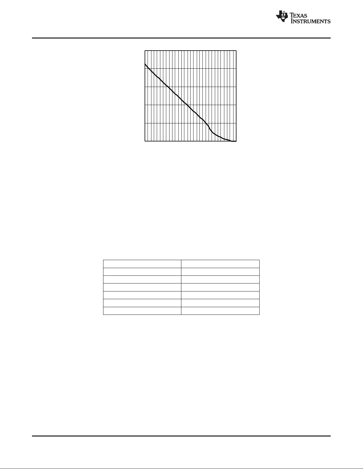
COMPACT LAYOUT
Parasitic inductance can be reduced by keeping the power path components close together and keeping the
area of the loops that high currents travel small. Short, thick traces or copper pours (shapes) are best. In
particular, the switch node (where L1, D1, and the SW pin connect) should be just large enough to connect all
three components without excessive heating from the current it carries. The LM3404/04HV operates in two
distinct cycles whose high current paths are shown in Figure 32:
Figure 32. Buck Converter Current Loops
The dark grey, inner loop represents the high current path during the MOSFET on-time. The light grey, outer loop
represents the high current path during the off-time.
GROUND PLANE AND SHAPE ROUTING
The diagram of Figure 32 is also useful for analyzing the flow of continuous current vs. the flow of pulsating
currents. The circuit paths with current flow during both the on-time and off-time are considered to be continuous
current, while those that carry current during the on-time or off-time only are pulsating currents. Preference in
routing should be given to the pulsating current paths, as these are the portions of the circuit most likely to emit
EMI. The ground plane of a PCB is a conductor and return path, and it is susceptible to noise injection just as
30 Submit Documentation Feedback Copyright © 2006–2013, Texas Instruments Incorporated
Product Folder Links: LM3404 LM3404HV
Page 31

LM3404, LM3404HV
www.ti.com
SNVS465F –OCTOBER 2006–REVISED MAY 2013
any other circuit path. The continuous current paths on the ground net can be routed on the system ground plane
with less risk of injecting noise into other circuits. The path between the input source and the input capacitor and
the path between the recirculating diode and the LEDs/current sense resistor are examples of continuous current
paths. In contrast, the path between the recirculating diode and the input capacitor carries a large pulsating
current. This path should be routed with a short, thick shape, preferably on the component side of the PCB.
Multiple vias in parallel should be used right at the pad of the input capacitor to connect the component side
shapes to the ground plane. A second pulsating current loop that is often ignored is the gate drive loop formed
by the SW and BOOT pins and capacitor CB. To minimize this loop at the EMI it generates, keep CBclose to the
SW and BOOT pins.
CURRENT SENSING
The CS pin is a high-impedance input, and the loop created by R
be made as small as possible to maximize noise rejection. R
SNS
, RZ(if used), the CS pin and ground should
SNS
should therefore be placed as close as possible
to the CS and GND pins of the IC.
REMOTE LED ARRAYS
In some applications the LED or LED array can be far away (several inches or more) from the LM3404/04HV, or
on a separate PCB connected by a wiring harness. When an output capacitor is used and the LED array is large
or separated from the rest of the converter, the output capacitor should be placed close to the LEDs to reduce
the effects of parasitic inductance on the AC impedance of the capacitor. The current sense resistor should
remain on the same PCB, close to the LM3404/04HV.
Table 1. BOM for Design Example 1
ID Part Number Type Size Parameters Qty Vendor
U1 LM3404 LED Driver SOIC-8 42V, 1.2A 1 TI
L1 SLF10145T-470M1R4 Inductor 10 x 10 x 4.5mm 47µH, 1.4A, 120 mΩ 1 TDK
D1 CMSH2-40 Schottky Diode SMB 40V, 2A 1 Central Semi
Cf VJ0805Y104KXXAT Capacitor 0805 100 nF 10% 1 Vishay
Cb VJ0805Y103KXXAT Capacitor 0805 10 nF 10% 1 Vishay
Cin C3225X7R1H335M Capacitor 1210 3.3 µF, 50V 1 TDK
Co C2012X7R1E105M Capacitor 0805 1.0 µF, 25V 1 TDK
Rsns ERJ8BQFR33V Resistor 1206 0.33Ω 1% 1 Panasonic
Ron CRCW08051333F Resistor 0805 133 kΩ 1% 1 Vishay
Table 2. BOM for Design Example 2
ID Part Number Type Size Parameters Qty Vendor
U1 LM3404HV LED Driver SOIC-8 75V, 1.2A 1 TI
L1 DO5022P-334 Inductor 18.5 x 15.4 x 7.1mm 330 µH, 1.9A, 0.56Ω 1 Coilcraft
D1 CMSH1-60M Schottky Diode SMA 60V, 1A 1 Central Semi
Cf VJ0805Y104KXXAT Capacitor 0805 100 nF 10% 1 Vishay
Cb VJ0805Y103KXXAT Capacitor 0805 10 nF 10% 1 Vishay
Cin C4532X7R2A225M Capacitor 1812 2.2 µF, 100V 1 TDK
Co C3216X7R2A154M Capacitor 1206 0.15 µF, 100V 1 TDK
Rsns ERJ6BQFR43V Resistor 0805 0.43Ω 1% 1 Panasonic
Ron CRCW08051184F Resistor 0805 1.18 MΩ 1% 1 Vishay
Copyright © 2006–2013, Texas Instruments Incorporated Submit Documentation Feedback 31
Product Folder Links: LM3404 LM3404HV
Page 32

LM3404, LM3404HV
SNVS465F –OCTOBER 2006–REVISED MAY 2013
www.ti.com
REVISION HISTORY
Changes from Revision E (May 2013) to Revision F Page
• Changed layout of National Data Sheet to TI format .......................................................................................................... 31
32 Submit Documentation Feedback Copyright © 2006–2013, Texas Instruments Incorporated
Product Folder Links: LM3404 LM3404HV
Page 33

PACKAGE OPTION ADDENDUM
www.ti.com
PACKAGING INFORMATION
Orderable Device Status
LM3404HVMA/NOPB ACTIVE SOIC D 8 95 Green (RoHS
LM3404HVMAX/NOPB ACTIVE SOIC D 8 2500 Green (RoHS
LM3404HVMR/NOPB ACTIVE SO PowerPAD DDA 8 95 Green (RoHS
LM3404HVMRX/NOPB ACTIVE SO PowerPAD DDA 8 2500 Green (RoHS
LM3404MA/NOPB ACTIVE SOIC D 8 95 Green (RoHS
LM3404MAX/NOPB ACTIVE SOIC D 8 2500 Green (RoHS
LM3404MR/NOPB ACTIVE SO PowerPAD DDA 8 95 Green (RoHS
LM3404MRX/NOPB ACTIVE SO PowerPAD DDA 8 2500 Green (RoHS
(1)
The marketing status values are defined as follows:
ACTIVE: Product device recommended for new designs.
LIFEBUY: TI has announced that the device will be discontinued, and a lifetime-buy period is in effect.
NRND: Not recommended for new designs. Device is in production to support existing customers, but TI does not recommend using this part in a new design.
PREVIEW: Device has been announced but is not in production. Samples may or may not be available.
OBSOLETE: TI has discontinued the production of the device.
Package Type Package
(1)
Drawing
Pins Package
Qty
Eco Plan
(2)
& no Sb/Br)
& no Sb/Br)
& no Sb/Br)
& no Sb/Br)
& no Sb/Br)
& no Sb/Br)
& no Sb/Br)
& no Sb/Br)
Lead/Ball Finish
(6)
SN | CU SN Level-1-260C-UNLIM -40 to 125 L3404
SN | CU SN Level-1-260C-UNLIM -40 to 125 L3404
CU SN Level-3-260C-168 HR -40 to 125 L3404
CU SN Level-3-260C-168 HR -40 to 125 L3404
CU SN Level-1-260C-UNLIM -40 to 125 L3404
SN | CU SN Level-1-260C-UNLIM -40 to 125 L3404
CU SN Level-3-260C-168 HR -40 to 125 L3404
CU SN Level-3-260C-168 HR -40 to 125 L3404
MSL Peak Temp
(3)
Op Temp (°C) Device Marking
(4/5)
HVMA
HVMA
HVMR
HVMR
MA
MA
MR
MR
(2)
Eco Plan - The planned eco-friendly classification: Pb-Free (RoHS), Pb-Free (RoHS Exempt), or Green (RoHS & no Sb/Br) - please check http://www.ti.com/productcontent for the latest availability
information and additional product content details.
TBD: The Pb-Free/Green conversion plan has not been defined.
Pb-Free (RoHS): TI's terms "Lead-Free" or "Pb-Free" mean semiconductor products that are compatible with the current RoHS requirements for all 6 substances, including the requirement that
lead not exceed 0.1% by weight in homogeneous materials. Where designed to be soldered at high temperatures, TI Pb-Free products are suitable for use in specified lead-free processes.
Pb-Free (RoHS Exempt): This component has a RoHS exemption for either 1) lead-based flip-chip solder bumps used between the die and package, or 2) lead-based die adhesive used between
the die and leadframe. The component is otherwise considered Pb-Free (RoHS compatible) as defined above.
Green (RoHS & no Sb/Br): TI defines "Green" to mean Pb-Free (RoHS compatible), and free of Bromine (Br) and Antimony (Sb) based flame retardants (Br or Sb do not exceed 0.1% by weight
in homogeneous material)
(3)
MSL, Peak Temp. - The Moisture Sensitivity Level rating according to the JEDEC industry standard classifications, and peak solder temperature.
5-Feb-2014
Samples
Addendum-Page 1
Page 34

PACKAGE OPTION ADDENDUM
www.ti.com
(4)
There may be additional marking, which relates to the logo, the lot trace code information, or the environmental category on the device.
(5)
Multiple Device Markings will be inside parentheses. Only one Device Marking contained in parentheses and separated by a "~" will appear on a device. If a line is indented then it is a continuation
of the previous line and the two combined represent the entire Device Marking for that device.
(6)
Lead/Ball Finish - Orderable Devices may have multiple material finish options. Finish options are separated by a vertical ruled line. Lead/Ball Finish values may wrap to two lines if the finish
value exceeds the maximum column width.
Important Information and Disclaimer:The information provided on this page represents TI's knowledge and belief as of the date that it is provided. TI bases its knowledge and belief on information
provided by third parties, and makes no representation or warranty as to the accuracy of such information. Efforts are underway to better integrate information from third parties. TI has taken and
continues to take reasonable steps to provide representative and accurate information but may not have conducted destructive testing or chemical analysis on incoming materials and chemicals.
TI and TI suppliers consider certain information to be proprietary, and thus CAS numbers and other limited information may not be available for release.
In no event shall TI's liability arising out of such information exceed the total purchase price of the TI part(s) at issue in this document sold by TI to Customer on an annual basis.
5-Feb-2014
Addendum-Page 2
Page 35

PACKAGE MATERIALS INFORMATION
www.ti.com 29-May-2013
TAPE AND REEL INFORMATION
*All dimensions are nominal
Device Package
LM3404HVMAX/NOPB SOIC D 8 2500 330.0 12.4 6.5 5.4 2.0 8.0 12.0 Q1
LM3404HVMRX/NOPB SO
Power
LM3404MAX/NOPB SOIC D 8 2500 330.0 12.4 6.5 5.4 2.0 8.0 12.0 Q1
LM3404MRX/NOPB SO
Power
Type
PAD
PAD
Package
Drawing
DDA 8 2500 330.0 12.4 6.5 5.4 2.0 8.0 12.0 Q1
DDA 8 2500 330.0 12.4 6.5 5.4 2.0 8.0 12.0 Q1
Pins SPQ Reel
Diameter
(mm)
Reel
Width
W1 (mm)
A0
(mm)B0(mm)K0(mm)P1(mm)W(mm)
Quadrant
Pin1
Pack Materials-Page 1
Page 36

PACKAGE MATERIALS INFORMATION
www.ti.com 29-May-2013
*All dimensions are nominal
Device Package Type Package Drawing Pins SPQ Length (mm) Width (mm) Height (mm)
LM3404HVMAX/NOPB SOIC D 8 2500 367.0 367.0 35.0
LM3404HVMRX/NOPB SO PowerPAD DDA 8 2500 367.0 367.0 35.0
LM3404MAX/NOPB SOIC D 8 2500 367.0 367.0 35.0
LM3404MRX/NOPB SO PowerPAD DDA 8 2500 367.0 367.0 35.0
Pack Materials-Page 2
Page 37

DDA0008B
MECHANICAL DATA
MRA08B (Rev B)
www.ti.com
Page 38

Page 39

IMPORTANT NOTICE
Texas Instruments Incorporated and its subsidiaries (TI) reserve the right to make corrections, enhancements, improvements and other
changes to its semiconductor products and services per JESD46, latest issue, and to discontinue any product or service per JESD48, latest
issue. Buyers should obtain the latest relevant information before placing orders and should verify that such information is current and
complete. All semiconductor products (also referred to herein as “components”) are sold subject to TI’s terms and conditions of sale
supplied at the time of order acknowledgment.
TI warrants performance of its components to the specifications applicable at the time of sale, in accordance with the warranty in TI’s terms
and conditions of sale of semiconductor products. Testing and other quality control techniques are used to the extent TI deems necessary
to support this warranty. Except where mandated by applicable law, testing of all parameters of each component is not necessarily
performed.
TI assumes no liability for applications assistance or the design of Buyers’ products. Buyers are responsible for their products and
applications using TI components. To minimize the risks associated with Buyers’ products and applications, Buyers should provide
adequate design and operating safeguards.
TI does not warrant or represent that any license, either express or implied, is granted under any patent right, copyright, mask work right, or
other intellectual property right relating to any combination, machine, or process in which TI components or services are used. Information
published by TI regarding third-party products or services does not constitute a license to use such products or services or a warranty or
endorsement thereof. Use of such information may require a license from a third party under the patents or other intellectual property of the
third party, or a license from TI under the patents or other intellectual property of TI.
Reproduction of significant portions of TI information in TI data books or data sheets is permissible only if reproduction is without alteration
and is accompanied by all associated warranties, conditions, limitations, and notices. TI is not responsible or liable for such altered
documentation. Information of third parties may be subject to additional restrictions.
Resale of TI components or services with statements different from or beyond the parameters stated by TI for that component or service
voids all express and any implied warranties for the associated TI component or service and is an unfair and deceptive business practice.
TI is not responsible or liable for any such statements.
Buyer acknowledges and agrees that it is solely responsible for compliance with all legal, regulatory and safety-related requirements
concerning its products, and any use of TI components in its applications, notwithstanding any applications-related information or support
that may be provided by TI. Buyer represents and agrees that it has all the necessary expertise to create and implement safeguards which
anticipate dangerous consequences of failures, monitor failures and their consequences, lessen the likelihood of failures that might cause
harm and take appropriate remedial actions. Buyer will fully indemnify TI and its representatives against any damages arising out of the use
of any TI components in safety-critical applications.
In some cases, TI components may be promoted specifically to facilitate safety-related applications. With such components, TI’s goal is to
help enable customers to design and create their own end-product solutions that meet applicable functional safety standards and
requirements. Nonetheless, such components are subject to these terms.
No TI components are authorized for use in FDA Class III (or similar life-critical medical equipment) unless authorized officers of the parties
have executed a special agreement specifically governing such use.
Only those TI components which TI has specifically designated as military grade or “enhanced plastic” are designed and intended for use in
military/aerospace applications or environments. Buyer acknowledges and agrees that any military or aerospace use of TI components
which have not been so designated is solely at the Buyer's risk, and that Buyer is solely responsible for compliance with all legal and
regulatory requirements in connection with such use.
TI has specifically designated certain components as meeting ISO/TS16949 requirements, mainly for automotive use. In any case of use of
non-designated products, TI will not be responsible for any failure to meet ISO/TS16949.
Products Applications
Audio www.ti.com/audio Automotive and Transportation www.ti.com/automotive
Amplifiers amplifier.ti.com Communications and Telecom www.ti.com/communications
Data Converters dataconverter.ti.com Computers and Peripherals www.ti.com/computers
DLP® Products www.dlp.com Consumer Electronics www.ti.com/consumer-apps
DSP dsp.ti.com Energy and Lighting www.ti.com/energy
Clocks and Timers www.ti.com/clocks Industrial www.ti.com/industrial
Interface interface.ti.com Medical www.ti.com/medical
Logic logic.ti.com Security www.ti.com/security
Power Mgmt power.ti.com Space, Avionics and Defense www.ti.com/space-avionics-defense
Microcontrollers microcontroller.ti.com Video and Imaging www.ti.com/video
RFID www.ti-rfid.com
OMAP Applications Processors www.ti.com/omap TI E2E Community e2e.ti.com
Wireless Connectivity www.ti.com/wirelessconnectivity
Mailing Address: Texas Instruments, Post Office Box 655303, Dallas, Texas 75265
Copyright © 2014, Texas Instruments Incorporated
 Loading...